Note : Les descriptions sont présentées dans la langue officielle dans laquelle elles ont été soumises.
CA 02221315 1997-11-17
1
SEMICONDUCTOR DEVICE
FIELD OF THE INVENTION
The present invention relates to a semiconductor device
and more specifically to a semiconductor device for use in
extremely thin, inexpensive IC cards with high bending
resilience, wireless multi-chip modules and mobile
communication terminals.
BACKGROUND OF THE INVENTION
An IC card with the cross structure shown in Fig. 20 is
described in "Data Carrier, II", pages 137 to 194, Japan
Industrial Press Corporation, issued March 15, 1991.
In the card, as shown in Fig. 20, a thick condenser
chip 411 mounted on a board 410 is connected through a bonding
wire 416 to a printed wiring board 412 and is then molded with
resin 415. The resulting structure is incorporated into the
center core 413, of which the top and bottom are covered with
over-sheets 409, 414.
Furthermore, Japanese Patent Laid-open No. Hei 3-87299
proposes an IC card comprising a slim chip.
In a conventional type card having the structure shown
in Fig. 20, elements such as a condenser chip 411 are so thick
CA 02221315 1997-11-17
2
that these elements are subject to the stress of bending and
are therefore, disadvantageously, readily broken.
With reference to the card proposed by the Japanese
Patent Laid-open No. Hei 3-87299, as shown in Fig. 8, the
surface and back face of a condenser chip 41 bonded to a thick
board 42 are stressed by a stretch or press operation if the
board is bent, such that a larger stress is applied to the
condenser chip 41 (of 200 ~,m thickness). Therefore, the
connection between a metallized pattern 43 and the condenser
chip 41 connected to the pattern 43 fails; or the condenser
chip 41 weak to mechanical stress because of its thinness, is'
readily broken through the stress. Hence, the reliability of
the condenser chip 41 is particularly low.
A card of conventional structure using a condenser
chip 41 is fabricated by attaching the condenser chip 41 onto
a thin card 42 which is readily bendable, followed by wire
bonding. Therefore, the card has low reliability because the
condenser chip 41 is easily broken. Additionally, the number
of process steps for mounting is large making it difficult to
reduce the production cost.
SUMMARY OF THE INVENTION
An object of the present invention to overcome the
problems of the prior art and provide a highly reliable,
inexpensive semiconductor device able to endure the stress of
bending, particularly a thin semiconductor device functioning
CA 02221315 2005-11-22
3
as an IC card, a multi-chip module or a mobile
communication terminal.
Certain exemplary embodiments can provide a
semiconductor device comprising: a flexible first card
board and a flexible second card board, the two boards
being placed to face each other at a given interval, and an
integrated circuit, a condenser and a coil all formed
between the first and second card boards, wherein the
thickness of the integrated circuit, the condenser and the
coil is 110 ~,m or less, and the upper and lower faces of
the integrated circuit, condenser and coil are positioned
within 55 gum above and below the neutral surface of the
semiconductor device if the semiconductor device has a
thickness of 0.76 mm or less, but within 9.5 ~.m above and
below the neutral surface of the semiconductor device if
the semiconductor device has a thickness of 0.5 mm or less,
and within 2 N,m above and below the neutral surface of the
semiconductor device if the semiconductor device has a
thickness of 0.25 mm or less.
Embodiments provide a semiconductor device comprising:
a condenser chip having a thickness of 110 ~,m or less; an
integrated circuit chip having a thickness of 110 ~.m or
less coupled with said condenser chip; and first and second
flexible substrates interposing said condenser chip and
integrated circuit chip between them.
Embodiments provide a semiconductor device comprising:
a flexible first substrate; a condenser chip having a
thickness of 110 ~m or less and disposed over said flexible
first substrate connected therewith by using conductive
paste; an integrated circuit chip coupled with said
CA 02221315 2005-11-22
3a
condenser chip; and a flexible second substrate disposed
opposite to said flexible first substrate so that said
condenser chip and said integrated circuit chip are disposed
between said flexible first and second substrates.
Embodiments provide a semiconductor device comprising:
a condenser chip having a thickness of 110 ~m or less; an
integrated circuit chip coupled with said condenser chip;
and flexible first and second substrates, and a thin plate
harder than said flexible first and second substrates so as
to cover said condenser chip.
Embodiments provide a semiconductor device comprising:
a condenser chip having a thickness of 110 N,m or less; an
integrated circuit chip coupled With said condenser chip;
and first and second flexible substrates interposing said
condenser chip and said integrated circuit chip between
them, wherein said condenser chip is disposed in said
semiconductor device so that a neutral plane of said
semiconductor device is disposed between an upper surface
and a lower surface of said condenser chip.
Embodiments provide a semiconductor device comprising:
a condenser chip having a thickness not greater than 110 ~m
and including a circuit element portion and a condenser
portion; a coil of a thickness not greater than 110 ~m which
provides energy to said condenser portion; and first and
second substrates interposing said condenser chip and coil
between them.
CA 02221315 2005-11-22
3b
Embodiments provide a semiconductor device comprising:
a circuit element portion; and a condenser portion, wherein
a condenser chip having a thickness not greater than 110 ~Cm
and first and second flexible substrates are disposed in
said condenser portion so that said condenser chip is
interposed between said first and second flexible substrates
and is covered with a thin plate harder than said first and
second flexible substrates.
Embodiments provide a semiconductor device comprising:
a condenser chip having a thickness not greater than 110 ~m
and having a circuit element portion and a condenser
portion; first and second flexible substrates interposing
said condenser chip between them; and a photograph disposed
over at least one of said first and second flexible
substrates.
Embodiments provide a semiconductor device comprising:
a condenser chip having a thickness not greater than 110 ~m
and including a circuit element portion and a condenser
portion; a coil having a thickness of 110 ~,m or less and
providing energy to said condenser portion; and first and
second flexible substrates interposing said condenser chip
and said coil between them, wherein a neutral plane of said
semiconductor device is positioned between upper and lower
surfaces of said condenser chip.
Embodiments provide a semiconductor device comprising:
a condenser chip having a thickness not greater than 110 ~.m
CA 02221315 2005-11-22
3c
and including a circuit element portion and a condenser
portion; first and second flexible substrates interposing
said condenser chip between them; and a thin plate harder
than said first and second flexible substrates, wherein a
neutral plane of said semiconductor device is positioned
between upper and lower surfaces of said condenser chip.
Embodiments provide a semiconductor device comprising:
a condenser chip having a thickness not greater than 110 um
and including a circuit element portion and a condenser
portion; first and second flexible substrates interposing
said condenser chip between them; and a photograph disposed
over a portion of a surface of at least one of said first
and second flexible substrates, wherein said portion is
located at a position which corresponds to a position of
said condenser chip, and wherein said condenser chip is
disposed in said semiconductor device such that a neutral
plane of said semiconductor device is positioned between
upper and lower surfaces of said condenser chip.
Embodiments provide a semiconductor device comprising:
an integrated circuit chip having a thickness of 110 ~m or
less; a coil which is coupled with a thin-thickness
condenser, said coil and said thin-thickness condenser
having a thickness of 110 ~.m or less; and first and second
flexible substrates interposing said integrated circuit
chip, said coil, and said think-thickness condenser between
them.
CA 02221315 2005-11-22
3d
Embodiments provide an IC card comprising: a condenser
chip having a thickness not greater than 110 ~,m and
including a circuit element portion and a condenser portion;
a coil having a thickness of 110 ~,m or less and providing
energy to said condenser portion; and first and second
flexible substrates interposing said condenser chip and said
coil between them, wherein a neutral plane of said IC card
is positioned between upper and lower surfaces of said
condenser chip.
Embodiments provide an IC card comprising: a condenser
chip having a thickness not greater than 110 ~,m and
including a circuit element portion and a condenser portion;
first and second flexible substrates interposing said
condenser chip between them; and a thin plate harder than
said first and second flexible substrates, wherein a neutral
plane of said IC card is positioned between upper and lower
surfaces of said condenser chip.
Embodiments provide an IC card comprising: a condenser
chip having a thickness not greater than 110 ~,m and
including a circuit element portion and a condenser portion;
first and second flexible substrates interposing said
condenser chip between them; and a photograph disposed over
a portion of a surface of at least one of said first and
second flexible substrates, wherein said portion is located
at a position which corresponds to a position of said
condenser chip, and wherein said condenser chip is disposed
CA 02221315 2005-11-22
3e
in said IC card such that a neutral plane of said IC card is
positioned between upper and lower surfaces of said
condenser chip.
Embodiments provide a card-shaped semiconductor device
comprising: a condenser chip having a thickness not greater
than 110 N.m and including a circuit element portion and a
condenser portion; a coil having a thickness of 110 ~m or
less and providing energy to said condenser portion; and
first and second flexible substrates interposing said
condenser chip and coil between them, wherein said first and
second flexible substrates are bonded together with
adhesive, and wherein a neutral plane of said card-shaped
semiconductor device is positioned between upper and lower
surfaces of said condenser chip.
Embodiments provide a card-shaped semiconductor device
comprising: a condenser chip having a thickness not greater
than 110 ~m and including a circuit element portion and a
condenser portion; and first and second flexible substrates
interposing said condenser chip between them, wherein said
first and second flexible substrates are bonded together
with adhesive, wherein said condenser chip is strengthened
by using a thin plate harder than said first and second
flexible substrates, and wherein a neutral plane of said
card-shaped semiconductor device is positioned between upper
and lower surfaces of said condenser chip.
Embodiments provide a card-shaped semiconductor device
comprising: a condenser chip having a thickness not greater
CA 02221315 2005-11-22
3f
than 110 N.m and including a circuit element portion and a
condenser portion; and first and second flexible substrates
interposing said condenser chip between them, wherein at
least one of the surfaces of said card-shaped semiconductor
device is printed, wherein said first and second flexible
substrates are bonded together with adhesive, and wherein
said condenser chip is disposed in said card-shaped
semiconductor device such that a neutral plane of said card
shaped semiconductor device is positioned between upper and
lower surfaces of said condenser chip.
More specifically, according to various embodiments,
the thickness of the integrated circuit, the condenser or
the coil is defined as 110 ~.m or less, provided that the
lower limits of the thickness of the card and the condenser
are 50 ~~,m and 0.1 hem, respectively. If the card thickness
is smaller than 50 ~,m, the flexibility of the card is
distinctly increased which creates difficulty in putting the
card to practical use; and it is also difficult to fabricate
a condenser of a thickness of smaller than 0.1 ~.m.
By fixing the integrated circuit, the condenser or the
coil at such a small thickness, the integrated circuit, the
condenser or the coil is able to endure the stress of
bending. When these are connected to a thin board such as
IC card with a flexible adhesive, a highly reliable IC card
resilient to the stress of bending can be produced.
CA 02221315 1997-11-17
4
If the card is slim, it is readily bent. So as to
release the stress of the condenser chip, the condenser chip
should be thin. For preparing a slim condenser more precise
apparatuses for fabricating such a condenser are required.
Thus, the thinness of the condenser to be fabricated should
be assessed from both the standpoints of economical efficiency
and procurement of reliability.
A given correlation in thickness between the card and the
condenser chip is present; by fixing both the card and the
condenser chip at the aforementioned thickness, various cards
resilient to bending and highly reliable can be produced at
a low cost. It is needless to say that this is the case with
the thickness of the coil and the integrated circuit placed
internally in the card, in addition to the thickness of the
condenser.
BRIEF DESCRIPTION OF THE DRAWINGS
Fig. 1 is a cross sectional view explaining Example 1 of
the present invention;
Fig. 2 is a cross sectional view explaining the
Example 1 of the present invention;
Fig. 3 is a cross sectional view explaining the
Example 1 of the present invention;
Fig. 4 is a plane view explaining the Example 1 of the
present invention;
CA 02221315 1997-11-17
Fig. 5 is a cross sectional view explaining the
Example 1 of the present invention;
Fig. 6 is a cross sectional view explaining Example of
2
the present invention;
5 Fig. 7 is a plane view explaining Example the
3 of
present invention;
Fig. 8 is a cross sectional view explaining the problems
of conventional cards;
Fig. 9 is a cross sectional view explaining the
Example 3 of the present invention;
Fig. 10 is a cross sectional view explaining the
Example 3 of the present invention;
Fig. 11 is a cross sectional vi ew explaining Example
4
of the present invention;
Fig. 12 is a cross sectional view explaining the
Example 4 of the present invention;
Fig. 13 is an explanatory view of the Example 4 the
of
present invention;
Fig. 14 is an explanatory view of the Example 4 the
of
present invention;
Fig. 15 is an explanatory view of the Example 4 the
of
present invention;
Fig. 16 is a plane view explaining Example 5 of the
present invention;
Fig. 17 is a plane view explaining Example 6 of the
present invention;
CA 02221315 1997-11-17
6
Fig. 18 is a cross sectional view explaining Example 7
of the present invention;
Fig. 19 is a plane view explaining the Example 7 of the
present invention;
Fig. 20 is a cross sectional view depicting one example
of conventional cards; and
Fig. 21 is a cross sectional view depicting one example
of conventional cards.
DETAILED DESCRIPTION OF EMBODIMENTS OF THE PRESENT INVENTION
Owing to the thinness of the condenser it is possible to
wire the condenser and the card by means of a conductive
paste. Accordingly, compared with conventional wire bonding
by means of a gold wire, a slim, flat IC card can be produced
at large scale at a low material cost . A structure comprising
such a slim condenser can be applied to the fabrication of not
only IC cards but also to other devices of similar shapes and
to multi-chip mounting.
Example 1
Fig. 1 is a cross sectional view explaining Example 1 of
the present invention.
As shown in Fig. l, a condenser 303 and a coil 305 are
bonded onto the surface of a card board 301 with conductive
material film 302 (Trade name; Anisolm, manufactured by
Hitachi Chemicals, Co.).
CA 02221315 1997-11-17
7
Because the thickness of the condenser 303 is as thin as
about 1 to 10 Vim, the condenser 303 can be readily bonded to
the surface of the board 301 by using the conductive material
film 301 in paste or ink-like liquid because the difference
in level between the surface of the board 301 and the
condenser 303 bonded to the board 301 is so small.
Therefore, the optimum card shape can be formed due to
such flat connection at an extremely small height. The
conductive material film 302 in paste is about 10 ~m in
thickness, with higher flexibility, so the film is
characteristically resilient to bending and resistant to a
difference in the thermal expansion coefficient.
The condenser chip 303 is formed as follows.
Firstly, as shown in Fig. 2, a lamination film 310
comprising an oxide film and a single crystal silicone film
is formed on a silicone board 311 to fabricate the SOI
(silicone on insulator) wafer.
Then, as shown in Fig. 3, the condenser 303 having a
lower electrode 307, an isolation film 308 and an upper
electrode 309 is fabricated on the main surface side of the
SOI wafer by a well-known semiconductive process. In the
lower electrode 307 use is made of thermally resistant
titanium and platinum and in the isolation film 308 use is
made of a film comprising a material with a larger dielectric
constant, such as PZT (solid solution of lead zirconia and
lead titanate).
CA 02221315 1997-11-17
8
Subsequently, selective etching by means of an aqueous
40 o KOH (potassium hydroxide) solution is done to remove the
silicone board 311, to subsequently fabricate the structure
shown in Fig. 3. Because the oxide film formed on the
silicone board 311 then functioned as a stopper of etching,
the lamination film 310 comprising the silicone film and the
oxide film could be left while the silicone board 311 was
selectively removed. Consequently, the condenser 303
comprising the electrode 307, the isolation film 308 and the
electrode 309 is structurally formed on the thin lamination
film 310.
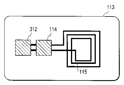
By fabricating a slim integrated circuit 312 and printed
coil 115 as a conductive pattern by a well-known process, the
card 113 of the plane structure shown in Fig. 4 is formed.
The conductive pattern coil 115 is formed by the printing
process used in the present example, but a coil formed by
processes other than the printing process may also be
satisfactory.
The coil 115 generates a dielectric electromotive force
on receiving electromagnetic waves from the outside, to supply
energy to the slim condenser 114. The coil 115 and the
condenser 114 are adhered in close proximity to the integrated
circuit 310 with a conductive paste or an anisotropic
conductive adhesive, so that the coil 115 and the
condenser 114 are electrically connected together. The
coil 115 also functions to transmit information data supplied
CA 02221315 1997-11-17
9
from outside of the card 113 to the condenser 114 and to
transform the data from the condenser 114 into electromagnetic
waves and transfer the waves to the outside of the card 112.
A communications card which is contactless and highly
reliable, can be produced by forming the card 112 of the
structure described above.
Because electrodes are placed on the surface of cards
(called contact type among conventional cards); contact
failure can occur or the cards may be weak to electrostatic
force. The present invention may be satisfactorily applied
to conventional contact-type cards.
Flexible adhesive 119, for example silicone, is filled
into the space formed by the condenser 114, the integrated
circuit 312 and the coil 115 fabricated by the printing
process as shown in Fig. 5. Additionally, the upper cover
sheet 117 and the lower cover sheet 118 are fixed with the
adhesive 119, to form a card of the cross structure shown in
Fig. 5.
The adhesive 119 has the double operation of adhesion and
envelopment so the thin-film condenser 114 and the like are
enclosed and retained within the soft gummous material. Very
little stress is loaded onto the surface of the condenser 114.
Therefore, the resulting card is resilient to bending.
Even if the card deforms when the card is subjected to
pin-point shock force, the force from outside is released
CA 02221315 1997-11-17
through the adhesive layer 119, which prevents stress attack
on the surface of the condenser 114.
Example 2
In the present example, an extremely slim condenser is
5 placed on the neutral surface of cards. By putting the
condenser between the two cards, a satisfactory bending
resilience was procured in this example.
As shown in Fig. 6, in the present example, a slim
element 315, for example a condenser chip, and a coil are
10 fixed between an upper card board 317 and a lower card
board 318 by means of an adhesive 314. By individually
arranging thin plates 313, 316 comprising a harder material
than these card boards 317, 318 on these card boards, the
element is reinforced.
The element 315 is at a thickness of 1 to 110 ~,m, which
is far thinner than the thickness of conventional elements;
therefore, by arranging the element 315 on the neutral
surface, the element is reinforced by the thin plates 313,
316, whereby satisfactory bending resilience is procured and
the card surface can be prepared to be flat.
Example 3
Fig. 7 depicts a plane placement in which another example
of the present invention to produce a card with better bending
resilience than conventional cards will be explained.
CA 02221315 1997-11-17
11
As shown in Fig. 7, in the present example, a slim
element 315, for example a condenser chip, and a coil are
placed inside a circle 321 where the diameter is equal to the
short side's length of card 319 and where the center thereof
is placed at the center of the card 319. It is observed that
the immunity to bending is thereby improved, and it is found
that the resulting card can be used in a far more simple
manner than conventional ones.
Fig. 9 depicts an example wherein a slim condenser is
used as the slim element 315 and the condenser 315 is embedded
at the center position 37 of the card board 36.
On a cross section of the bent card 36, expansion forces
are induced on the surface of the curved board, while
compression forces are induced on the back face. Because no
compression occurs at the central part of the cross section
of the card 36 under stress, the stress loaded onto a slim
condenser chip can be released; if the condenser chip 315 is
placed on the central part of the card.
When the card board 36 is bent, the surface and back face
thereof are both stressed by a stretch or press operation.
Because the condenser 315 is placed at the center position 37
of the card board 36, the condenser 315 is never attacked by
such stress. Thus, a highly reliable card resilient to
bending is produced.
So as to form a card of the structure shown in Fig. 9,
a condenser 315 is attached on the surface of card board 39,
CA 02221315 1997-11-17
12
as shown in Fig. 10. Then, card board 36 of the same
thickness as that of the card board 39 is attached onto
the condenser 315, whereby the structure shown in Fig. 9 can
be readily formed. The condenser 315 may be placed at a
desirable position inside the circle 321 shown in Fig. 7, in
addition to the center position of the board 39.
Example 4
Fig. 11 is a view explaining another example of the
present invention, depicting the state of a card with a
curvature due to bending stress.
Because the thin condenser chip 104 is put between a
lower piece of card board 103 and an upper piece of card
board 101 along a center line 102a of the cross section of the
two boards, such a structure will be less influenced by
bending. Thus, the condenser chip 104 is not stressed. When
the card is bent, the condenser chip 104 is also bent, but the
stress then is extremely small because the condenser chip 104
is extremely thin.
Fig. 12 shows the case where the condenser chip 104 is
bent. When the condenser chip 104 is bent, the surface stress
p of the condenser chip 104 is represented, as follows,
according to Navier's theorem: p - E X t/R; where E
represents Young's modulus of the condenser; R represents the
radius of curvature; and t represents 1/2 of the thickness of
the condenser chip 104.
CA 02221315 1997-11-17
13
Because the surface of the condenser chip 104 comprises
silicone oxide, E is equivalently equal to the Young's modulus
of the silicone oxide. The above formula indicates that the
surface stress of the condenser chip 104 is proportional to
the thickness of the condenser chip 104, but inversely
proportional to the radius of curvature R. When the surface
stress of the condenser chip 104 is larger than the mechanical
toughness of the condenser chip 104, the chip is broken
through bending. Because the radius of curvature R is
infinite in the absence of any bending, the surface stress P
is zero; when R gets smaller following the progress of
bending, the stress p gets larger until the condenser
chip 104 is broken finally.
However, if the condenser chip 104 is thin, the surface
stress p is reduced, even through bending with the same
radius of curvature R; therefore, the condenser chip 104 can
get sufficiently resilient to bending if the condenser
chip 104 is made thinner within a range not exceeding the
limit against mechanical breakage.
However, if the condenser chip 104 is made very thin, it
is difficult to handle. Thus, as shown in Fig. 11, the
condenser 104 is put between two card boards 102, 103
comprising plastics, metal and the like, whereby the condenser
CA 02221315 1997-11-17
14
is readily handled. Then, most preferably, the
condenser chip 104 is placed on a neutral surface 102a of
card 101. By such placement, the neutral surface of the
condenser 104 agrees with the neutral surface 102a of the
card 101 with zero stress even when the card is bent, so that
the condenser chip 104 is possibly never broken even if the
card 101 is bent, as in the case that only the condenser
chip 104 is singly bent.
Fig. 13 shows the results of the determination of the
dependency of the surface stress in the LSI (Large Scale
Integration) chip on the ratio of the LSI chip thickness to
the card thickness, using as the parameter the card thickness.
After placing the slim condenser on the neutral surface of the
card board, the surface stress of the condenser is determined,
corresponding to the ratio of the thickness of the condenser
to the card thickness.
The LSI chip surface stress has a significant relation
with the degree of the curvature of the card; the degree of
the curvature of the card varies largely, depending on the
thickness and materials of the card, and the force loaded onto
the card, and the position of the card. In the present
example, an LSI chip is placed at the center position of the
plane face of the card; as the card material, vinyl chloride
CA 02221315 1997-11-17
commonly used for general magnetic cards and credit cards is
used. Because PET (Polyethylene Terephthalate) material is
characteristically harder and is less easily bent than vinyl
chloride, the results recovered by using vinyl chloride are
5 applicable to any card comprising other materials including
PET.
The radius of curvature defining the degree of bending
varies depending on the bending moment loaded on the card.
The bending moment is loaded onto the card, up to a limit
10 above which the card is bent and folded over. The radius of
curvature at the center of a vinyl chloride card of a
thickness of 0.76 mm is 50 mm. Provided that the thickness
of the LSI chip is the same as the thickness of the card
herein, the surface stress of the LSI chip is calculated by
15 the formula 8E12 X 0.38/50 (Pa), according to the
aforementioned formula of stress, which is 600 MPa. The
Young's modulus of glass cited from the Japanese Scientific
Table was used because the surface of the LSI chip is
principally composed of silicone oxide film layer, it is
assumed that the surface has the same physical properties as
those of glass.
The moment of inertia of the card is involved in the
relation between the radius of curvature and the thickness of
CA 02221315 1997-11-17
16
the card. The radius of curvature R is represented by
E X I/M, wherein E represents the Young's modulus of the card;
I represents the moment of inertia; and M represents bending
moment. Because the moment of inertia of the card is
proportional to the cube of the thickness of the card, the
profile curve of the radius of curvature, as shown in Fig . 15 ,
is prepared. Fig. 15 shows that the surface stress of the LSI
chip is 2.5 GPa and 5.4 GPa at card thickness of 0.5 mm and
0.25 mm, respectively, provided that the ratio of the
thickness of the LSI chip to the card thickness is 1Ø At
that state, the LSI chip is readily broken, but in accordance
with the present invention, the LSI chip fabricated to be thin
is put between the neutral surfaces of the cards. Therefore,
such a break can be prevented.
Using the ratio of the thickness of the LSI chip to the
card thickness as a parameter, the surface stress of the
resulting slim condenser is measured. The results are shown
in Fig. 13. An enlarged view of a part of Fig. 13 is shown
in Fig. 14, wherein the ratio of the thickness of the LSI chip
to the card thickness is 0 to 0.16.
In Fig. 14, the stress of the LSI chip resilient to
bending is 90 MPa, which is the value cited from the Japanese
Scientific Table, provided that the break strength of the LSI
CA 02221315 1997-11-17
17
chip is assumed to be equal to the break strength of glass.
Thus, the necessary thickness of the LSI chip and the lowest
thickness limit of the LSI chip at various dimensions of card
thickness can be determined in Fig. 14. More specifically,
any break of the LSI chip due to card bending absolutely never
occurs, provided that the thickness of the LSI chip is 110 ~.m
or less with a card thickness of 0.76 mm; or that the
thickness of the LSI chip is 19 ~.m or less with a card
thickness of 0.5 mm; or that the thickness of the LSI chip is
4 ~.m or less with a card thickness of 0.25 mm.
It is needless to say that the reliability of the LSI
chip is improved when the thickness of the LSI chip is as thin
as the lowest limit, but the limit of the thickness of the
chip to be possibly fabricated is almost 0.1 ~.m. The
fabrication of any LSI chip thinner than the limit is
difficult.
The LSI chip and the slim condenser are most preferably
placed in such a manner that the neutral surfaces of the LSI
chip and the condenser might agree with the neutral surface
of the card. However, the upper or lower faces of the LSI
chip and the condenser are satisfactorily placed within the
upper or lower faces of an LSI chip and a condenser being
individually of the lowest thickness limits defined by the
CA 02221315 1997-11-17
18
card thickness and being placed on the neutral surface of the
card.
More specifically, the upper or lower face of the slim
integrated circuit, the slim condenser or the coil is
satisfactorily positioned within 55 ~,m above or below the
neutral surface of the card provided that the thickness of the
card on completion is 760 ~.m or less, or within 9.5 ~,m above
or below the neutral surface of the card provided that the
thickness of the card on completion is 500 ~.m or less, or
within 2 ~,m above or below the neutral surface of the card
provided that the thickness of the card on completion is
250 ~.m or less.
In the preferred embodiments, the thickness of a
semiconductor device (namely the card on completion) and the
thickness of the integrated circuit, the condenser or the coil
are 760 ~.m and 110 ~,m, respectively; or 500 ~,m and 19 Vim,
respectively; or 250 ~m and 4 ~,m, respectively.
Example 5
Fig. 16 shows another example of the present invention.
A slim condenser may possibly be provided with various
control functions. More specifically, as described above, the
SOI wafer and the well-known semiconductive process are used
CA 02221315 1997-11-17
19
to fabricate a circuit device part 323 and a condenser
part 324 adjacent to each other, in a slim condenser 322,
whereby various controls can be included. in one chip and high
performance and a low cost can be established. For example,
a circuit device part 323 can be utilized for data storage in
wireless cards.
Example 6
Fig. 17 depicts another example of the present invention.
In accordance with the present invention, slim elements such
as a condenser chip are put between two card boards to
fabricate a-card; therefore, the card surface is very flat.
A card comprising conventional thick elements is weak to
bending on the surface of which difference in level of up to
150 ~,m may be formed, so that it is difficult to make the card
flat until the difference is reduced to 30 ~.m, which is
essential for the pressure-sensitive printing process. So as
to make the surface flat, the structure should be so highly
precise that the cost therefor is eventually escalated.
However, in accordance with the present invention,
various elements such as a condenser chip are extremely thin
and the surface is flat, as described above. Therefore, as
shown in Fig. 17, the slim element 326 can be placed below
CA 02221315 1997-11-17
a picture 327, in the present example, whereby the degree of
freedom is improved.
Example 7
Fig. 18 shows the cross structure of a card, on the
5 surface of which printing is effected; a printing material 328
is placed so that the material might be hung or held over the
slim element 332. In the structure, the element 332 is thin
and embedded in an adhesive 331, and a upper cover sheet 329
and a lower cover sheet 330 are bonded together with the
10 adhesive 331. Thus, the surface turns flat.
Therefore, even when a printing roll reaches the top of
the edge of the element 332, the pressure is dispersed, with
no occurrence of breakage of the element 332. A photograph
of the cardboard can be printed on the surface of the upper
15 cover sheet 329 or lower cover sheet 330, for example. In
this case, the part of the photograph is handled gently, so
the element 332 can be placed at a desirable position.
Fig. 19 is a view depicting the plane structure of the
card shown in Fig. 18, wherein printing material 332 effects
20 predetermined printing over the element 332 placed on a
card 333. Conventionally, the element 332 has been broken
frequently in such a structure. In the present example,
CA 02221315 1997-11-17
21
however, the element 332 is extremely thin as described above
that predetermined printing could be effected with no concern
of breakage. A card having relatively simple structure can
be produced at a high reliability.
As apparent in the description above, the following
advantages can be brought about in accordance with the present
invention.
1. High reliability because of no concern of breaking due to
bending.
2. Easy production at low cost because of the simple
structure.
3. Because the condenser is extremely thin, the board and
the condenser can be wired with a conductive paste, with the
resulting lower cost and additionally with the resulting flat
surf ace .
4. An extremely slim condenser can be produced by the use of
SOI wafer, with less concern about breaking due to bending.