Note : Les descriptions sont présentées dans la langue officielle dans laquelle elles ont été soumises.
CA 02224SlS 1997-10-28
WO96/35194 PCT~S95/07578
Advanced Method of Indicating Incoming Threat Level
RELATION TO OTHER PATENT APPLICATIONS
This patent application is a continuation-in-part (C-I-P) of
the United States Patent Application Serial Number 08/433,819
entitled "Advanced Method of Indicating Incoming Threat Level To An
Electronically Secured Vehicle and Apparatus Therefor" filed
05/04/95; and, it is a continuation-in-part (C-I-P) of the United
States Patent Application Serial Number 08/112,940 filed 08/03/93,
entitled "Method Of Indicating The Threat Level Of An Incoming
Shock To An Electronically Secured Vehicle and Apparatus Therefor";
and, a continuation-in-part (C-I-P) of Patent Application Serial
Number 07/945,667, entitled "Advanced Automotive Automation And
Security System" filed 09/16/92.
r~ UND OF THE INVENTION
Field of the Invention
This invention pertains to the field of electronic security
systems that detect unwanted intrusions into secured areas and
sound an audible alarm in response thereto. More particularly, the
invention pertains to a method of differentiating between a high
degree of intrusion or threat such as a shock or a
low intensity degree of intrusion or insubstantial threat, received
by the protected structure or object, and e~ecuting an appropriate
alarm as well as preventing nonphysical, random energy inputs from
tripping the security alarm.
Description of the Prior Art
Electronic security systems have been used for some years and
their popularity increases as the national crime rate continues to
climb. Most such systems, especially those used for protection of
automobiles, include a controller, a series of intrusion sensors
--1--
SUBSTITUTE SHEET (RUL~ 26)
CA 02224~1~ 1997-10-28
WO96/35194 PcT~S95/07578
for detecting attempted intrusions through doors, hood, and
windows, an alarm for activation upon receipt of a signal or
signals from the sensors indicating an attempted unwanted entry
into the vehicle, and a power source, normally the vehicle battery,
to power the system and sound the alarm. Other components are
often included such as automatic resetting circuits and shut-down
devices for use when the alarm needs to be deactivated. These
systems may be original equipment on new vehicles or retrofitted on
existing vehicles.
The security systems may be effected by a nonphysical signals,
or electrical surges commonplace in the automobile circuitry. The
inte~e~ armi~g and disarming of an alarm ~ystem is usually
performed by S~n~; ng a digitally coded signal, by a hand-held
transmitter operated by one or more push buttons. In addition,
other such systems may be armed by mere passage of time following
the driver's act of turning off the engine and exiting the vehicle
with the doors and windows closed and after a short time interval
such as thirty ~30) seconds. Thereafter the system may be disarmed
by a ha~d-held transmitter or by a delay circuit that activates the
alarm if the system is not disarmed by the driver upon entry into
the vehicle. The first type of Ar~; ng is known as "active arming"
while the latter is known as "passive ~r~ing~.
Upon detection of an attempted intrusion into the vehicle by
one of the sensors, the alarm is activated for a period of time,
for instance thirty (30) seconds to one (1) minute, and then, if
the alarm has not been ~;sArme~ by the remote transmitter or by the
manipulation of a "kill" switch, mounted interior the vehicle,
usually in a hidden area therein, the alarm response tPrm;nAtes or
times-out and the security system is once again reset to monitor
the sensors and triggers.
One form of such a sensor is called a "shock" sensor. The
shock sensor technology of this lnvention is discussed in
Applicants' Patent Application Number 08/112,940. However, a
number of other sensors may be employed within the alarm system of
this invention. This invention includes, but is not limited to, the
--2--
SUBSrITUTE StlEET (RULE 26)
CA 02224~1~ 1997-10-28
WO96t35194 PCT~S95107578
application of shock sensors, motion sensors, field disturbance
sensors, sound discriminators, ultrasonic sensors, current sensors
and other sensors which sense disturbance or threat applied to or
about an area and generate an electrical signal in response
thereto. An ;nCom;ng threat to the protected area such a vehicle
includes threats such as physical impact, activity in or about the
vehicle, breach of the vehicle electric syste_, the sound of
breAki n~ glass, or other activity results in the sensing of the
activity and generation of an electrical signal which is then
interpreted by the alarm controller to generate an alarm
response.
Certain problems exist with conventional security systems that
render their usage less than desirable under certain ci.~u~Lances.
For example, a shopping cart inadvertently bumped ~;nct the
vehicle will usually cause a full alarm response. While the alarm
is certainly necessary to alert the owner, inadvertent tripping of
the alarm is annoying and could result in either the owner becoming
frustrated, and thereafter not activating the alarm, or convi~in~
the shopper or other car owners that such a loud, annoying alarm is
not what they want in their vehicles.
In other situations, certain transient electric fields can
invade the circuitry of the alarm system and generate enough of a
signal to trip the alarm even in the absence of intrusion to the
secured area. When a warn signal is generated by the alarm, it
flashes the running lights which generates electrical surges or
transients. These transients may generate electrical signals which
may feed into the alarm circuitry where they are amplified and trip
full alarm. In other situations, such as where a cellular
telephone is used about the vehicle, the initial surge of the
wireless tr~n~m;ssion signal may be sufficient to generate an
actuation level signal resulting in the activation of the alarm.
Still further, in isolated cases, such as where a police car parks
behind a protected area and the officer "keys" the microphone on
his radio, the surge from his transmitter could interact with the
anti-theft system induction coil and produce a false alarm.
--3--
SUBSllTllT~ SHEET (RULE 26
CA 02224~1~ 1997-10-28
WO96/35194 PCT~S95/07578
Still further, there are instances where a disturbance
continlleC unabated after the initial activation of the alarm
sequence. For instance, a vehicle parked next to a train station
may receive an alarm input generated by a p~C;ng train. The alarm
will commence and term;n~te after rllnn;ng its course, yet often the
train has not passed completely by the vehicle. I~ the prior art,
the alarm will sound again because of the continuous input of
energy from the train. This can be of annoyance to others in the
area.
Crowded parking lots are prime areas for car theft. In these
cases, dissatisfaction with the anti-theft system may cause the
owner to cease arming the system thus rendering the vehicle subject
to theft. This condition, if not corrected, may cause other vehicle
owners to cease purchA~in~ such security systems for fear of
annoying others and thereby und~rr;n~ the desirability for and
effectiveness of anti-theft devices.
What is nPeAp~ to circumvent the drawbacks heretofore
described is (l) a vehicle security system capable of
differentiation between a light, generally non-threatening
intrusion event and a stronger, usually security-threatP~;ng
intrusion event to the vehicle and output a pulse to the alarm
circuit appropriate to the degree of intrusion about the secured
area, and (2) a vehicle security system that will discriminate
between the non-threatening events and block them or otherwise
divert the signals they produce so that an alarm is not generated.
SUMMARY OF THE INVENTION
This invention is a novel method of de~l; ng with these
problems and discriminating between the degree of threat from the
;n~o~;ng intrusion sensors. ~or e~ample, the alarm system of this
invention generates a mild audible chirp in the event one lightly
touches a protected vehicle while loading groceries in a parking
lot. Conversely, a full alarm response is generated if the car is
towed or a crow-bar applied to its e~terior. The low intensity
alarm is called a "warn-away" and is of a serious, but far quieter
-4-
SUBSrIME SHEET (RULE 2~)
CA 02224~1~ 1997-10-28
WO96/35194 PCTIUS~S11~7~
nature and will generally generate the proper message of alarm
presence to the intruder without engaging the full alarm. The
person inducing the threat is thereby quietly, but convincingly
advised by prerecorded voice or a series of soft chirps of the
li~;ted intrusion he or she has caused, ~ithout activation of ear
piercing audible alarm response. Further, the owner and other
people are not disturbed or embarrassed by a full alarm response
caused by an innocent individual.
In addition, this invention includes the novel feature of
providing full wave rectification of the output signal from the
sensor and ignoring the first few milliseconds of the signal
produced. Additionally, the present invention requires the signal
to drop to its zero (0) level or reference voltage before
triggering warning alarm. This allows an alarm condition to be
registered only upon sensing actual intrusions on or about the
protected area, as compared with non-physical intrusions generated
by EMF or RF fields about the protected area. These features
therefore eliminate the spurious signals that are produced by
nonphysical threat conditions.
Most security systems involve only half-wave rectification of
the induced signal emanating from the sensor. In the event the
signal generated by a sensor generates a signal having positive and
negative components the signal and in the event there is only
partial rectification of the signal. The resulting rectified
signal would be of unnaturally low value and not be an accurate
reproduction or indication of the full intensity or degree of the
incoming threat to the protected area. This practice is consistent
with sensors employed to trigger the alarm system, but is
unacceptable to the present invention which looks at the degree of
the intrusion. Thus, to determine the degree of the intrusion
sensed by a sensor, the present invention analyzes the peak to peak
value of the sensor signals to determine the true degree of
intrusion.
The method and apparatus disclosed herein analyzes the signal
produced by various sensors having the capability of generating an
-5-
SUBSlITUTE SHEET (RULE 2~)
CA 02224~1S 1997-10-28
W O96135194 PCTrUS9S/07578
electric signal upon sensing an intrusion event. Depending on the
strength or value of the sensor signal, a mild or low intensity
degree of intrusion generates a pulse having a short pulse-width
generating a warn-away alarm that will automatically reset itself
without requiring intervention by the ~ehicle owner. The same
method and apparatus is capable of generating a longer pulse-width
pulse which generates both a mild, warn-away alarm response as well
as a stronger, full alarm response.
When the low threat level, "warn-away" pulse is generated by
the alarm system, the alarm system of this invention continlles to
monitor its sensors and is capable of immediate activation of a
full alarm upon sensing a high degree of intrusion as reported by
one or more of its sensors, even while a warn-away alarm is being
given. If two or more mild shocks are received by the vehicle
within a finite tLme period, seven (7) seconds for example, the
system will produce a full alarm, whereas if the mild shocks are
repeated on a sequence longer in time than seven (7) seconds, a
second and repeated "warn-away~ alarm will be produced again.
The prior art alarm system have not yet appreciated these
features and continue to generate repeated "warn-away" or full
alarms. In fact, in some cases the energy dispensed in the
"warn-away" alarm is of sufficient magnitude to generate a
low-threat level input that triggers another "warn-away" alarm so
that the system continues to cycle "warn-away~ alarms each induced
by the preceding alarm.
Further, this invention contains the unique property of
ignoring the first few milliseconds of signal produced by a sensor.
A real threat condition usually lasts far longer than the ignored
duration and the energy level of the residual signal is sufficient
to pass through an integrator to a comparator to determine the
relative degree of the threat. The signals produced by RF bursts,
EMF bursts and other non-threatening or non-physical pheno-m~non
typically do not last beyond that period and still cause a threat
situation. Accordingly, those signals produced by non-physical
a~d/or non-threatening phPnomPnon will be disregarded and will not
-6-
SUBSrlT~JTE SHEET (RULE 263
CA 02224~1~ 1997-10-28
WO96~5194 PCT~S95/07578
cause the alarm systems to enter into an alarm condition.
To overcome the problem of repeated sirens during periods of
extended sensor input, such as in the train passing example, or
even when a truck or other heavy vehicle passes the parked car,
means are provided to prevent repeated alarms as long as the
initial input remains within a given intensity for an ext~n~e~
time. For instance, as long as the intensity level of the input
signal remains rather constant following cessation of the full
alarm signal, the circuit will not process another sensor input
until this signal disappears and reappears again. This means that
the prolonged motion the train passing nearby a protected vehicle,
which generates a sensor input, will not cause the alarm to sound
again and again. This feature also prevents continuous alarm
outputs in those cases where the sensor is in a state of a
continuous output. The state of continuous sensor output may be
mechAn;cal in nature ~the train e~ample) or from electrical
distllrhAnces .
In a second embodiment of this invention, the circuit is
designed such that fewer wires need be used to attach the sensor to
the alarm giving rise to a savings in material and reduction in
installation time and trA; n; ng.
The prior art has recognized some of these problems, however,
to date there has been little success achieved in solving them. In
the patent to Hwang, (U. S. Patent 5,084,967) a "motion detector"
is allegedly connected to a pair of signal amplifier circuits that,
upon receipt of a long signal or a series of short pulses from the
detector, will sound a "full" alarm whereas, upon receipt of a
shorter pulse signals, will sound a "pre-entry warning", lesser in
severity than the "full" alarm. However, this patent discloses
that the "detector" is a t;~ dependent switch. Therefore the
degree of threat is determined by its duration, not its physical
degree. The schematic of the Hwang device shows the use of
components that are arranged as a switch to turn on and off a
transistor to allow the detected signal pass on to the alarm
warning device. ~hus, there is no comparison of the "level of
--7--
SUBS~TUT~S~EE~(RUL~26)
CA 02224~1~ 1997-10-28
WO96135194 PCT~S95/07578
intensity" of the signal, but merely the "duration" of the signal.
This is not an accurate assessment of the degree of threat sensed
by the sensor and reproduced into an electrical signal and does not
differentiate between "intensities" of the physical and
non-physical inputs. Moreover, the output signal from the device of
Hwang Patent proceeds directly to the siren, whereas the device of
the present invention interposes another device, the alarm control
module or alarm controller, that determines what level of alarm is
generated.
Accordingly, the main object of this invention is a method and
apparatus for use on about an electronically secured area that
responds differently to different degrees of threat sensed by the
sensors arranged therein. Other objects of the invention include
a method and apparatus that has at least two levels of intensity
deterr;nAtion, one for a low degree of threat received by the
vehicle to produce a pulse that may be used to trigger a warning of
a stronger alarm, should the threat not be discontinued, and a
separate pulse that may be used to trigger a stronger, louder alarm
for non-discontinued light shocks and stronger shocks; a method and
apparatus for producing a pulse that may be used to trigger a
warn-away audible alarm that may be repeatedly sounded to signify
the vehicle is under electronic security while not producing a
pulse that may trigger the loudest alarm so as to r;n;~; 7-e the
disturbance to those nearby in the event of a non-threatening
2S disturbance received by the vehicle; a method and apparatus that
maintains readiness to produce a pulse that may be used to trigger
an audible alarm even while a warn-away alarm message is being
used; a method and apparatus for detecting a signal produced by a
non-physical assault on the vehicle, such as by a burst of RF
energy or EMF energy, and for removing it from interaction in the
system circuitry; a method and apparatus that provides full wave
rectification of the induced signal to provide a more accurate
analysis of the threat inducing the sensor signal; an apparatus
which does not continue to sound an alarm in the event a generally
constant and continuous disturbance such as a moving train; an
-8-
SUBSTITUTE SHEET ~RUI ~ 26)
CA 0222451~ 1997-10-28
WO96/35194 . PCT~S95/07578
apparatus having the ability to co~llnicate the level of threat in
a pulsewidth of the sensor output pulse, thereby el;~;n~ting a
dedicated wire connection for each alarm stage; an apparatus that
may be retrofitted into existing vehicles as well as included as
original equipment on new vehicles; and, an apparatus that will
automatically rearm upon the completion of a measured length of the
warn-away or the full alarm; circuitry that can be maint~;ne~ in an
integrated circuit thereby providing economy of manufacture,
improved r-l;Ah;l;ty, space savings and less power consumption.
These and other objects of the invention may be obtained by reAA;ng
the following specification along with the drawings that are
appended hereto. The prote~tio~ sought by the inventor may be
gleaned from a fair re~;ng of the claims that conclude this
specification.
~SCPTPTION OF THE DRAWINGS
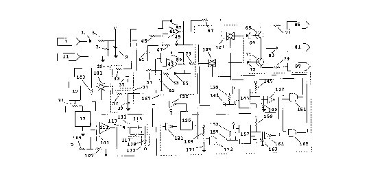
Figure l is a schematic diagram of the apparatus of this
invention;
Figure 2 is a flow diagram illustrating the operation of the
apparatus generally depicted in Figure l;
Figure 3 is a schematic diagram of an alternate embo~;rAnt of
the apparatus, showing less wiring needed to accomplish the same
functions as shown in Figure l;
Figure 4 is a schematic diagram of an alternate embodiment of
the bilateral switch wiring shown in Figure l;
Figure 5 is a schematic diagram of an alternate embodiment of
the bilateral switch wiring shown in Figure 3;
Figure 6 is a top level schcmatic representation of an
alternate embo~;rAnt of this invention;
Figure 7 is a top level block diagram of CMOS Integrated
Circuit a~d its analog and digital sections;
Figure 8 is an intermediate level block diagram of the analog
section, showing the amplifier block and the integrator block;
Figure 9 is a schematic/block diagram of the amplifier block
and its inverting/noninverting determ;n~tion circuitry;
Figure l0 is a schematic diagram of the amplifier block;
_g_
SUBSTITUTE SHEET (RUI E 26)
CA 02224~1~ 1997-10-28
WO96/35194 PCT~S95/07578
Figure ll is a schematic diagram of the warnaway alarm and
full alarm switching capacitor integrators and their associated
circuitry;
Figure 12 is an interr~iAte level block diagram of digital
section, showing its major blocks therein;
Figure 13 is a schematic of output timer block having six
timer blocks, timer clock divider block and the associated
circuitry required to support the timing of the IC;
Figure 14 is a schematic of the integrator disable control
circuit; and,
Figure 15 is a schematic of one of the five stage ~T-flip-
flop~ timers that is used in IC.
DESrPTPTION OF Th~ rk~r-~KK~ EMBODIMENT
The novel method of this invention for indicating the threat
level of an incoming threat to an electronically secured structure,
such as a vehicle comprises, the steps of sensing a threat
delivered to an area, generating an electric signal the strength of
which is proportional to the intensity of the threat, ignoring the
first portion of the signal so as to remove from further
consideration those disturbances that are non-physical or
non-threatening, analyzing the r~m~;ning signal to determine if it
is of a low, generally non-threatening intensity or of a higher,
generally security-threatening intensity, and producing either a
first pulse that triggers a low intensity "warn-away" alarm, or
separate first and second pulses, representing a signal cont~;n;ng
both the low intensity and higher intensity components, that
trigger both a low and a high intensity alarms. The step of
generating an electric signal includes generating an alternating
current signal whose amplitude and period is proportional to the
intensity of the physical shock. Figure l shows the apparatus of
this invention.
In Figure l the solid lines between components refer to
conductors and will not be individually numbered except where
necessary. Where conductors cross and the intersection is marked
--10--
~UBSTlTUTE Sl IEE~ ~RULE 26)
CA 02224~1~ 1997-10-28
WO 96135194 PcTIU~9~ 75/
with a dot or period, it is a junction; where one conductor crosses
another and the intersection has no dot or period, there is no
junction. As shown in Figure 1, an input voltage, generally in the
range of from about si~ to about eighteen volts d.c. is inputted
from a battery (not shown), such as a car battery or other source
of direct current, to an input terminal 1. The current is
regulated by a reverse flow protection diode 3, a surge l;~iting
resistor 5, an over-voltage protection Zener diode 7 and a filter
capacitor 9 to produce a steady flow of direct current. The ground
return enters at input term; nAl 11.
The sensors employed by the present invention are
interchangeable. Different sensors are employed for different
functions within the alarm system and their selection depends in
large by the anticipated environment within which the user expects
to keep the protected property. Some of the more common sensors
are shock sensors, motion sensors, field disturbance sensors, sound
discriminators, ultrasonic sensors and current sensors. T h e
shock sensors known in the art are mechanical, mercury movement,
magnetic induction, and piezo types. Applicants' Patent
Application 08/112,940 disclosed Applicant's preferred embodiment
of the shock sensor.
M~chAn;cal shock sensors use a weighted cone at the end of a
spring which makes electrical contact with a fixed pointer upon an
impact, creating an output pulse.
2~ Mercury sensors consist of two designs. The first design is
the mechanical contact type. The second design is one in which
mercury is suspended inside an inductor that is part of an
electronically tuned circuit. In both designs an impact results in
the mercury remaining in a fi~ed position, while everything else
moves a~out with the impacted vehicle.
The magnetic induction shock sensor uses a magnet suspended by
an elastic band such as rubber, silicon or spring near a high value
inductor. The inductor usually has an iron or ferrite core. An
impact moves the sensing inductor while the magnet remains fi~ed,
3~ creating an impact AC signal in the inductor. The signal is
~UBSnTUTE SHEET (RULE 26)
CA 02224~1~ 1997-10-28
wos6l35l94 PCT~S95/07578
typically amplified, detected, integrated and then compared with
preset levels to deterrine whether or not to generate an output
signal.
The piezo shock sensor uses a weighted piezo sensor. A
me~h~n;cal resonance of appro~imately seventy (70) hertz is created
by ~;ng mass to the piezo sensor. This aids in the detection of
impacts to the vehicle. Similarly, the weight remains fixed while
the balance of the piezo sensor moves about with the impact to the
vehicle.
Another type of sensor employable by this invention is a
motion sensor. Motion sensors sense very slow movements of the
vehicle. These movements could be caused by jArk; n~ lifting,
moving, or any other type of slow movement of the protected object.
These movements may be sensed by several methods such as a weighted
p~n~lllum with r?ch~n;cal or electronic contact, mercury movement
switch or mQCh~n; cal/electronic movement ~~PnS; ng devices, or any
other slow movement sensing system.
Another type of sensor employable by this invention includes
a field disturbance sensor. Field disturbance sensors sense motion
of objects such as the human body in a microwave radio frequency
field in or about the protected area. The presence of the moving
object disturbs the microwave field and creates a disturbance
therein. This results in a change of the sensor output signal.
This disturbance is both reflective and absorptive in that all
objects absorb and reflect RF energy. A multichannel sensor
generates an output signal proportional to intensity of the
detected disturbance. A single channel sensor only generates a
signal if the pre~ent threshold is exceeded. Additionally, a
pulsed microwave signal could be generated to look for time of
signal return. This, however, requires a more complex sensor and
circuit than the above field disturbance sensor.
Another type of sensor employable by this invention includes
a sound discriminator. Sound discriminator senses a high frequency
sound disturbance in or near the protected area and is normally
used to sense the breaking of glass and/or metal to metal sounds.
-12-
SUBSTlTUTE ~HEET (RUL~ 26)
CA 02224~1~ 1997-10-28
WO96/35194 PCT~S~ /s/~
The sensor normally uses an electric condenser microphone to sense
the sound and convert it to an AC signal. This AC signal is
amplified and processed through a high pass and/or band pass
filter~s). The signal is then detected and compared to preset
thresholds. An output pulse indicative of the intensity of the
disturbance is then generated and output.
Another type of sensor employable by this invention includes
an ultrasonic sensor. An ultrasonic sensor can work on the same
principle as the field disturbance sensor (doppler frequency
shift), but uses an ultrasonic sound field instead of an RF energy
field. In a second embodiment, the sensor uses an ultrasonic sound
generator ttransmitter) to set up a field of sound waves usually at
forty (40) kilohertz. An ultrasonic sensor (receiver) then detects
any dist~lrhAnce. This signal is then amplified and detected
generating an ouL~ pulse or pulses according to the level of
dist~lrh~nce. In a third embodiment, the ultrasonic sound could be
pulsed to measure the movement of and distance to the object
creating a disturbance.
Another type of sensor employable by this invention includes
a current sensor. Current sensors sense the change in battery
voltage caused by the activation of devices which in turn produces
a current load. There are at least two different types of current
sensors. One type senses only small changes in voltage created by
any load being turned on, while the second type detects a sudden
large change in voltage, such as a surge created by ;nc~n~escent
lights being turned on. The first type of sensor is simpler and
easier to manufacture, while the incandescent light sensor does not
require an e~ternal input to disable the circuit when the vehicle
automatic electrical cooling fans turn on. The current sensor is
usually employed to sense the under hood, trunk, and/or dome lights
turning on when an unauthorized entry is made.
Each and every sensor heretofore mentioned senses a particular
type of intrusion and produces an electrical signal proportional to
the degree of threat sensed. Other types and kinds of sensors
capable of sensing particular cond,itions and providing an
-}3-
SUBSIITUTE SHEET ~RULE 26)
CA 02224~1~ 1997-10-28
WO 96/35194 PCI~/U~ 7578
electrical signal in response thereto are not mentioned, but are
contemplated within the scope of this invention. The above
mentioned sensors will be collectively referred to as sensor means
12.
s The step of analyzing the signal to determine if it is of a
low or high intensity includes the first step of passing the signal
through a switching capacitor amplifier 19 to provide full wave
rectification, i.e., the negative portions of the signal are
converted to positive portions. Accordingly, the output of
amplifier 19 is always positive and will give an-appro~imately
equal output regardless of the polarity of sensor means 12 signal.
This overcomes the short~or;ngs of a sensor having a signal
operating in the positive and negative region in respect to the
system ground. This allows the entire dynamic range of the signal
to be offset/rectified to a positive voltage. The gain of
amplifier 19 is fixed at a predeterr;ne~ value. A potentiometer 23
is used to adjust the level of the i~put from sensor means 12.
A normally closed, analog, bilateral switch 101 is provided
and connected between amplifier 19 and an inverting cn~rator 111.
In other embodiments of the invention comparator 111 is not
inverting. It is opened for a predetermined amount of time such as
a few, i.e., S, milliseconds at the beqinn;ng of each pulse string,
as will be hereinafter more fully set forth, in order to cut off,
delete or disregard the first portion of the signal output from
amplifier 19. This cut off is employed to prevent extraneous,
non-physical energy surges, such as RF and/or EMF fields, as
hereinbefore described, from tripping the alarm.
Another significant feature of the present invention provides
for removal from consideration of signals which do not disappear
and later reappear. The signals which do not disappear and later
reappear are disregarded by this device to prevent continuous alarm
outputs which are a nuisance. This is particularly helpful where
the alarm system is operating in an area having e~posure to
ph~no~~non of prolonged duration such as a freight train passing
nearby the alarm system. As the train passes, it generates a
-14-
~UBSTITUTE SHEET (RULE 26)
CA 02224~1~ 1997-10-28
WO96~5194 PCT~S9S/07578
vibration which likely has an intensity sufficient to generate an
alarm. In practice, this type of disturbance is not well received
by alarm systems because the alarm system will generate an alarm
which ceases after a predetermined time and which is regenerated
again and again as long as the disturbance continues about the
area. This pro~ides for much frustration to the owner of the alarm
system and the people nearby, there~y reducing its effectiveness.
To overcome this problem, the alarm of the present invention
monitors the signal causing the alarm. In the event this
signal/distllrhAnce cont;ntl~C to be present at a generally constant
intensity for a time greater then the duration of the alarm
response, the second and subsequent alarm responses are not
generated until such time as the signal generated by the
disturbance disappears and then reappears again. In practice this
provides for one cycle of alarm response if the alarm system
detects a distl~rhAnce such as a moving train. The alarm response
will not be repeated over and over again until such time as the
distllrhAnce caused by the train disappears and then later
reappears.
Switch 101 is nn~; n~l ly in a closed position and is held
closed by the power supply voltage less voltage drop through
resistor 119. Shutting off or opening of switch 101 is
aCcomplishpA by use of an inverting comparator 111 and its
associated circuitry. Resistors 105 and 107 establish a reference
voltage for comparator 111. Resistor 103 and capacitor 109 filter
out high frequency transients on the input to comparator 111. In
the event a continuous high frequency signal is present at the
input of sensor means 12 or at the output of amplifier 19, the high
frequency filter 103 and 109 could lead to a continuous, low DC
signal output at the output of comparator 111. This inhibits
clocking of D flip-flop 125 which in turn opens switches 127 and
129 until the output of comparator 111 changes state and produces
a clock signal at the clock input of D flip-flop 125.
As a signal inputted to comparator 111 goes high, the output
of comparator 111 goes low and is coupled through a diode 113 and
-15-
SllBSTlTUTE SHEET (RULE 26)
CA 02224~1~ 1997-10-28
WO 96135194 PCT/U:,9~,J'~7
a capacitor llS to switch 101. Therefore the source voltage for
keeping switch 101 in its closed position is shorted for a
predeterri ne~ duration of time through capacitor 115, which
provides for opening of switch 101 for that duration of time. By
adjusting the capacitance of capacitor 115, a delay, such as 5
~ill;ceconds is required to charge capacitor 115 in order to turn
bilateral switch 101 back on. Resistor 117 is provided as the
discharge resistor for capacitor 115 and its value is chosen so
that capacitor 115 will not discharge for several hundred
m; 11; ~econds so as not to interrupt the signal pulse string. The
discharge time of cAp~c;tor 115 is such that only the first few
milliseconds of any pulse string is allowed to be coupled through
capacitor 115 and diode 113 to shut off analog bilateral switch
101 .
The next step, after passing the amplified signal through
switch 101 is to input this amplified signal simultaneously to two
separate and i~dependent voltage integrators, 29 and 31, shown
within dotted line perimeters, that are connected in parallel to
the output of amplifier 19. Integrator 29 comprises a resistor 33
and a capacitor 35 while integrator 31 comprises a resistor 37 and
a capacitor 39. The ratio of sensitivity of integrators 29 and 31
is adiusted, by varying the resistance of resistors 33 and 37 and
varying the capacitance of capacitors 35 and 39 to the order of
approximately S:1 so that integrator 29 is appro~imately five times
as sensitive as integrator 31. This ratio can be varied outside of
5:1 under certain circumstances such as where the vehicle is
unusually large.
The next step is to send the output of integrators 29 and 31
to a pair of separate voltage comparators/pulse generators 41 and
43 that are equally referenced from input term~ nAl 1 . The
reference for voltage comparator 41 is established by resistors 45
and 47 and a diode 49 while the reference for voltage comparator 43
is established by resistors 51 and 53 and a diode 55. Another pair
of diodes 57 and 59 are used to latch the respective voltage
comparators 41 and 43 when their respective input signals exceed
-16-
SUBSTITUTE SHEET (RULE 26)
CA 02224~1~ 1997-10-28
WO96/35194 PCT~S95/07578
the comparator reference voltages.
The next step in this novel method is for the pulse generator
portion of comparators/generators 41 and 43 to output either a
first pulse from generator 41 representing a low intensity signal
or separate first and second pulses from both generators 41 and 43
representing a signal contA; n; n~ a low intensity and a high
intensity component. This is performed when voltage comparator 41
or 43 is latched through either diode 57 or diode 59 when the
; nro~; n~ signal from integrators 29 or 31 exceeds the reference
voltage thereto. Once latched, the respective comparator produces
an output pulse timed by resistor 45 and capacitor 61 with respect
to comparator/ pulse generator 41 or by resistor 51 and a cApAc;tor
63 with respect to comparator/pulse generator 43 to one of two
drive transistors 65 and 71.
Output drive transistor 6S receives the output pulse from
voltage co~rArator/pulse generator 41 through a resistor 67 and an
indicating light emitting diode 69 for the duration of the pulse
from generator 41. The other output drive transistor 71 receives
the output pulse from voltage comparator/pulse generator 43 through
a resistor 73 and an indicating light emitting diode 75 for the
duration of the pulse from generator 43. Resistors 77 and 79 are
current limiting resistors employed to protect transistors 65 and
71 respectively. The outputs are enabled by a ground placed on
term; n~l 81 through a diode 83. The outputs are fed respectively
to tPrm;nAl 85 to connect to a warn-away alarm circuit (not shown),
and to term;nAl 87, to connect to the full alert alarm circuit (not
shown). The output pulse for the warn-away alarm, from term;nAl 85,
may be set at one length, such as 200 milliseconds, and the output
pulse for the full alarm from t~rm;nAl 87 may be set at a different
length, such as appro~imately 1 full second.
The negative voltage, 5 millisecond pulse from comparator 111
is inverted by inverter 123. This provides a logic one pulse which
resets and holds in reset for the 5 m;ll;second period (determined
by capacitor 115) the "D flip-flopl' 125. This achieves the
function of discarding from consideration a continuous signal
-17-
SUBSTITUTE SHEET (RllLE 26)
CA 02224~1~ 1997-10-28
WO96/35194 PCT~S95~/a/~
having a frequency such that this signal represents a DC signal at
input of comparator 111. Thus, this signal will elim;nAte any
clock activity to D flip-flop 12S until such signal disappears a~d
again reappears. The "Q" output of 125 is connected to the inputs
of "AND GATES" lS1 and 16S, causes the outputs of lSl and 16S to go
low. The low signals at the outputs of 151 and 165 opens normally
closed analog bilateral switches 127 and 129. This prevents any
output from pulse generators 41 and 43 being coupled to output
transistors 6S and 71.
After the end of the 5 ~ isecond reset pulse, the "Q" output
at flip-flop 125 is set high by a clock signal created by
comparator 111. This clock pulse is inverted by inverter 121 to
present the proper input to the 125 clock input. The sensor
outputs 85 and 87 are now enabled for the duration of the output
pulse(s) created by pulse generators 41 and 43.
As mentioned before, this invention provides for the
embodiment where the alarm will not be continuously triggered by a
relatively constant threat signal which persists without
interruption. One application for this feature is an armed alarm
system which is triggered by a train. Ordinary alarm systems
continue to sound its warning for the duration of the threat
signal. The alarm system of the present invention provides for a
single cycle of alarm and does not sound the alarm again until the
threat signal disappears and again reappears. Therefore in the
example of the passing train, the alarm would sound for one cycle,
such as 2.S seconds for the warn-away and 30 seconds or a minute
for a full alarm, and as long as the train threat does not
disappear (i.e. the train passed) and again reappear (i.e. another
train appears) the system of the present invention will not sound
the alarm again. The following circuit provides this function.
Output bypass timers 143 and 157 are triggered and reset from
the trailing edge (negative going edge) of the output pulses from
41 and 43 respectively. The output of full alarm pulse generator
43 is applied to timer 157 via AND gate 173. When any input of an
AND gate goes low, its output goes low. All inputs of an AND gate
-18-
Sl~BSTITUTE SHEET (RULE 26)
CA 0222451~ 1997-10-28
WO96~S194 PCT~S95107578
must be high to get a high at its output. These triggers are
coupled to the inputs of timers 143 and 157 by coupling capacitors
141 and 155 respectively. Resistors 139 and 153 are pull-up
resistors on the trigger input of their respective timers.
Resistor 145 and capacitor 149 control the time that the
"warn-away" output is disabled. Resistor 159 and capacitor 163
control the time that the "alarm" output is disabled. When the
timers are triggered/reset, the timing capacitors 149 and 163 are
discharged, the outputs go high, and the timing cycle is started.
The outputs will go low at the end of the timing cycle.
The high output from warn-away bypass timer 143 is inverted by
inverter 147 and applied to AND gate 151. The low at the input of
151 causes the output of 151 to go low opening bilateral switch
127. This interrupts any output from 41 and disables the warn-away
output drive to output transistor 65. All warn-away outputs are
therefore disabled anytime that warn-away bypass timer 143 is
rllnn;n~. All repetitive triggers that occur inside the ti mi n~
window are bypassed ~disabled) on the warn-away output until the
warn-away bypass timer expires (appro~imately 1/2 second). While
the timer is r~lnn;ng, if the output at 41 goes low (output pulse
e~pires), the timing capacitor is discharged, and the timer is
restarted with a full charging cycle duration to run.
Full alarm bypass timer 157, upon receiving a negative pulse
from the trA;l; ng edge of the output pulse from 43 via AND gate
173, works identical to the warn-away bypass timer 143. The high
output from 157 is inverted by inverter 161 and applied to AND
gates 151 and 165. The low at the inputs of 151 and 165 causes the
outputs of 151 and 165 to go low. This low output in turn is
applied to the control input of bilateral switches 127 and 129.
Both output drives are interrupted, disabling both outputs (warn-
away and full alarm) for the duration of the full alarm output
bypass timer 157 (several seconds).
The full alarm bypass timer 157 is also used as a power up
reset timer. At power on capacitor 171 is fully discharged,
applying a low at the input of AND gate 173. Capacitor 171 is
--lg--
SUBSTtTUTE SHEET (RULE 26)
CA 02224~1~ 1997-10-28
WO96~5l94 PCT~S95/07578
slowly charged bias resistor 169 removing the low input from AND
gate 173. The output of 173 is low during this charging period
triggering full alarm bypass timer 157. Therefore, at power up,
both outputs are disabled for several seconds until timer 157 times
out.
Figure Z shows the flow of the induced sig~al and produced
pulse through the circuit of Figure 1. The sensor of sensor means
12 generates a signal the strength of which is proportional to the
intensity or degree of the threat. Amplifier 19 provides full wave
rectification and amplification of the signal for presentment
through switch 101 to integrators 29 and 31 in parallel for
integration of the total value of the pulse train less the first
part thereof cut off by switch 101. The respective sensiti~ities
of integrators 29 and 31 help to differentiate between a lower
degree of threat which is likely non-threate~ing in nature and a
higher degree of threat that represents a potential intrusion into
the vehicle. The separate voltage comparators/output pulse
generators 41 and 43 complete the differentiation and output a
pulse to the output indicator and driver that results in one or
both alarms being activated.
Amplifier 19, referenced by voltage from the car battery,
amplifies all signals received from the sensor means 12.
Integrators 29 and 31 ignore any signal whose peak-to-peak voltage
is equal to or less than the amplifier reference voltage. Hence,
very low signals generated by the sensor means 12 will not produce
a signal or signals sufficient to activate voltage
comparators/output pulse generators 41 and 43 to latch the
respective unit and produce a pulse to be sent on to output drive
transistors 65 and 71.
Upon receipt of a low degree threat signal, above the
reference level of amplifier 19, the circuit will operate to
activate voltage comparator 41, latch it, and produce a pulse that
will activate the warn-away alarm trigger output ~not shown)
through teT~;nAl 85. While this is going on, the circuit remains
fully prepared to receive and process other signals from the sensor
-20-
SUBSTITUTE SHEET (RULE 26)
CA 02224~1~ 1997-10-28
WO 96/35194 PCI'IUS95i~7~/8
means 12. In the event a high degree of threat is sensed by sensor
means 12 while the warn-away alarm is given, the security bre~chP~
alarm trigger output, will be tripped through terminal 87 and both
alarm outputs will be tripped or triggered simultaneously. In all
cases, both alarm trigger outputs are triggered when a high degree
of threat is received, unless at the time of the time of threat
input, war~-away output is di~abled by the bypass timer 143, while
only the warn-away alarm trigger output is tripped in response to
a low degree of threat.
This invention also carries the capability to drive the
vehicle's electronic security system~s audible or visual warning
devices directly or indirectly by use of an external control relay.
Since the warn-away output pulses are short (appro~imately 200
milliseconds) and could be enabled by the vehiclels electronic
security system, this greatly reduces the annoyance created by an
alarm system's full alarm. The output drivers have the capability
to drive output control circuits as long as a ground is applied to
~u~uL control terminal 81. These output pulses are fed through
output terrinAl~ 85 and 87 to directly or indirectly drive warning
devices.
Figure 3 shows an alternate embodiment of the invention.
~h~nging the timing of the full alarm pulse generator 43 to a range
greater then the warn-away 200 milliseconds allows for a
considerable reduction in the output circuitry. This also reduces
the installation time of the present invention. With a 200
millisecond warn-away output pulse and one second full alarm pulse,
these pulses can be outputted or multiple~ed on the same wire for
applying to one such input of the alarm control module. In the
same e~ample full alarm output pulse generator 43/timing capacitor
63 is changed to S times its normal value. The full alarm output
pulse time is therefore increased by a factor of 5.
The outputs from output pulse generators 41 and 43 are then
applied to the common output indicating LED 69 and output drive
transistor 65. This is accomplished through output drive current
limiting resistors 67 and 73 and analog bilateral switches 127 and
-21-
SUBSTITUTE SHEET (RULE 26)
CA 02224~1~ 1997-10-28
WO 96/35194 PCT/u5gJ~ S /~
129 connecting to a common conductor before re~ch; n~ LED 69.
Therefore the LED will indicate warn-away output with a short 200
r;ll ;cecond light output pulse and full alarm output with a longer
one second light output pulse. The output transistor 65 will be
s con~llcting, applying a ground or near ground potential to the
collector for 200 milliseconds for warn-away and for one second for
full alarm.
Figure 4 represents a modification to the preferred embodiment
shown in Figure 1 and shows the output of the 5 millisecond timer
131 inverting the signal, by inverter 123, and feeding the output
cignAl to two normally open, bilateral sttitches 100 and 102. The
signal closes switches 100 and 102 for the 5 r; 11; cecond period.
This keeps integrator capacitors 35 and 39 shorted out for the 5
millisecond time period. This represents another method of
h~n~l;ng the signal.
Figure 5 represents a modification to the preferred embodiment
shown in Figure 3 and also shows the output of the 5 m;ll;~econd
timer 131 to invert the signal, by inverter 123, and fee~;ng the
output signal to two normally open, bilateral switches 100 and 102.
The signal closes switches 100 and 102 for the 5 millisecond
period. This also ~eeps integrator capacitors 35 and 39 shorted
out for the 5 millisecond time period. This represents another
method of h~n~1 ;ng the signal.
Figure 6 a schematic representation of an alternate embodiment
of the of this invention. It is a schematic of a dual stage sensor
that uses a custom CMOS integrated circuit (IC). Figures 7 through
15 are block diagrams and schematics of this custom CMOS integrated
circuit. The schematic in Figure 6 is the schematic of sensor
means 12 being represented by a shock sensor 12. Although this
embodiment is hereafter described employing a shock sensor, any
sensor could integrate this device.
With the custom IC, there is substantial reduction in the
number of parts required to build the product and subsequently the
economic cost of the device. The part reduction is evident by the
comparison of the part count in the discrete component embodiment
-22-
SUBSTITUTE SHEET ~RULE 2~)
CA 02224~1~ 1997-10-28
Wo96~5194 PCT~S95tO7578
of Figure 5 and the device of the present embodiment shown in
Figure 6. The reduction in component count and their associated
cost of assembly, allows for a significant reduction in the cost of
the complete sensor unit.
A nominal plus 12.6 volts DC power source enters the sensor at
terminal 1 and returns through terminal 11 (common). The ~ulLe~L
from this power source is limited by current l;miting and filtering
resistor 5. Capacitor 9 along with resistor 5 filters the
transients in the power source. The voltage is then regulated down
to 5 volts by resistor 6, zener diode 7, and transistor 8.
Transistor 8, zener diode 7, and resistor 6 regulation method was
chosen to reduce current in the sensor or to reduce the cost.
Sensor 12 supplies an alternating current (AC) voltage output
indicative of the sensed input to the sensor (sound, vibration,
shock, movement (field distllrh~nce or ultrasonic sensor), motion,
or other input). Sensitivity of the complete sensor is adjusted
with potentiometer 23 by adjusting the proportionate input voltage
going to IC 201. IC 201 is a CMOS device limiting the frequency
input c~pAh; 1; ty of the integrated circuit. This limits the
frequency of the RF energy that can enter IC 201 through its input
circuitry. Capacitor 24 filters low frequency RF energy that may
be detected by any of IC 201 input circuitry; therefore, IC 201
e~ tes the requirement for having the signal appear, disappear,
and then reappear before the sensor will actuate the output.
Therefore IC 201 does not include circuitry of the other embodiment
which el; m; nAtes the DC signal resulting from RF energy feeding
into the device.
Resistor 34 establ;sh~s a 10 KHz nominal operating frequency
of the clock of IC 201. Although IC 201 operates at 5 volts and
the m~; mll~ operating voltage is 7 volts, the output is protected
to 17 volts by stacking the output transistors ~not shown) allowing
IC 201 to operate in a 12 volt system. Terminal 87 provides a
connection for a negative output while triggered on the full alarm
output and capacitor 78 provides protection to IC 201 from high
voltage transients such as static electricity. LED 69 provides a
-23-
SUBSTITUTE SHEET (RULE 26
CA 02224~1~ 1997-10-28
WO96~5194 PCT~S9S/07578
vi~ual signal of device triggering. In the preferred embodiment it
is energized for two seconds. LED 69 will flash at a 5 Hertz rate
during a warnaway trigger and is constantly on during the full
alarm trigger. The full alarm output signal is negative and the
warnaway output is positive. This provides for warnaway output to
drive output transistor 65 (required for driving a relay) through
base current limiting resistor 67. Transistor 65 then supplies a
negative pulse during the warnaway output to output terr;nA1 85.
In the preferred embodiment the output pulse is appro~imately 200
milliseconds for warnaway output and appro~imately 1.2 seconds for
a full alarm output. IC 201 provides both positive and negative
voltage outputs to the output ter~; n~ 1~ as they are required for
the application. Another version of this sensor 12 uses two
negative outputs from IC 201 to drive alarm inputs directly. The
positive output is used to drive a transistor, so that the alarm
system can chirp a siren using a relay, with the 200 millisecond
warnaway output.
Figure 7 is a top level block diagram of IC 201 showing its
major blocks, digital block 401, analog block 301 and its
connection pads. The IC of the preferred embodiment employs eight
pins. The logical configuration of this IC has 11 outputs however.
Therefore only eight of the eleven pins are brought out in any one
configuration. AVSS, the analog ground, is always term;nAted to
VSS, IC 201 ground terminal and its output is not brought out. As
stated above, both the full alarm output and the warnaway output
have positive and negative pads (pad is an output terminal on the
IC chip internal to IC 201), that can be terr;~Ated according the
requirements of the application. Only one of the full alarm and
one of the warnaway alarm outputs are brought out of IC 201.
Figure 8 is an intermediate level block diagram of analog
block 301 showing the major blocks of the analog section of the IC
201, amplifier block 303 and integrator block 305. The basic
inputs are shown on the left side and the outputs are shown on the
right side of the block diagram. PH1 through PH2B outputs, from
the clock of IC 201, drive all the functions of IC 201. VBIAS is
-24-
SUBSTITUTE SHEET (RULE 2~1
CA 02224~1~ 1997-10-28
W096/35194 PCT~S95tO7578
a bias for the CMOS analog circuitry of IC 201. PORB iS a power on
reset (bar or not). VIN is the input signal to amplifier block
303. AVSS iS the analog ground reference of IC 201. DISINTEG is
a disable the integrator signal from the digital block that uses
the amplifier output (AMPOUT) as a clock to initiate the DISINTEG
signal. WARNTR is the warnaway trigger output of the warnaway
integrator that is used to trigger the timed warnaway output of IC
201. AT A~MTR iS the full alarm trigger output of the full alarm
integrator that is used to trigger the timed full alarm output of
IC 201.
Figure 9 is a schematic/block diagram of amplifier block 303
showing amplifier 307 block, inverting/noninverting determ;n~tion
circuitry and voltage reference circuitry. The
inverting/noninverting circuitry provides outputs to effectively
rectify the input signal before it is input to the amplifiers.
Amplifier 307 block is described in Figure lO. VREF is establ; sheA
by a voltage divider made up by l90R ohm resistor 315, 5~ ohm
resistor 317, and 5R ohm resistor 319. VREF is stabilized by 5
picofarad capacitor 313 and micropower amplifier 321 connected as
voltage follower. VREF is at 125 millivolts (( 5/200) *5=0.125) .
The sensor signal is connected to the input of amplifier 309 which
uses VREF as a reference voltage. Amplifier 309 is an inverting
switching capacitor amplifier with a gain of 40 that uses clock
signals PHl through PH2B to control the switching of the amplifier
signals. A sim; lar amplifier is described below during the
disclosure of Figure lO. The output of amplifier 309 is then input
to comparator 311, which is referenced to VREF the same as
amplifier 309. Therefore any movement of the IC input signal
(sensor output signal) away from its zero reference will cause the
output of comparator 311 to go to full output polarity of the
signal. This is then input to the ~D" input of ~D-flip-flop~ 323.
One of the clock signals, PHlB, is used to clock this to output ~Q~
on the next clock cycle. PORB control signal resets ~D-flip-flop"
323 to a low output at power up. A logic high ~Q" output is used
as a INV control signal and a logic low signal is inverted by
- 25 -
Sl~BSTITUT~ SHEET ~RUL~ 26)
CA 02224~1~ 1997-10-28
WO96/35194 PCT~S95~7
inverter 325 and used as the NONINV control signal.
Figure 10 is a schematic of amplifier 307 block. It is a pair
of switching capacitor amplifiers with a total gain of 1600.
During phase 1 of the clock (PHl and PHlB), analog bilateral switch
335 is open and analog bilateral switches 337, 341, and 349 are
closed effectively shorting out both amplifiers 345 and 353, and
coupling the signal to the input of the amplifier input capacitor
339 through analog bilateral switch 331, if the signal is not
inverted (AVSS (ground) is connected), or analog bilateral switch
333 if the signal is inverted (VIN (input signal) is connected).
This places ground at the input and output ter~; n~l S of both
amplifiers 345 and 353, if the input is not inverted, or the level
of the signal if the input is inverted. The input signal is very
small in amplitude, therefore there is not a significant difference
at the output of the second amplifier 353 with either ground or the
signal connected.
During phase 2 of the clock (PH2 and PH2B), analog bilateral
switch 335 is closed and analog bilateral switches 337, 341, and
349 are open. This connects VIN (input signal) to the input of the
amplifiers if the signal is not inverted or connects AVSS (ground)
if the signal is inverted. This impresses a positive voltage equal
to the input signal across input capacitor 339 (20 picofarads) in
either case. If the signal is negative it is inverted by first
applying the input signal to amplifiers 345 and 353 while they are
shorted and then applying ground to input when they are in the
amplifying mode (phase 2). This rectifies the signal by always
placing a positive signal, with reference to the applied reference
that is applied during the none amplifying mode, to the input of
amplifier 345 during the amplifying phase (phase 2 of the clock).
Amplifier 345 has a gain of 40 because it will require 40
times the voltage across 0.5 picofarad capacitor 343 to e~ualize
the input voltage across 20 picofarad capacitor 339. The same is
true of amplifier 353 and 20 picofarad capacitor 347 and 0.5
picofarad capacitor 351. Amplifiers 345 and 353 are buffered CMOS
micropower amplifiers which are known in the art. Capacitor 354 is
-26-
SUBSTITUT~ S~tEET (RUL~ 26)
CA 02224~1S 1997-10-28
W O 96~5194 PCTrUS95/07578
a 5 picofarad filter capacitor on the 125 millivolt reference input
to amplifiers 345 and 353.
Figure 11 is a schematic of the warnaway and alarm switching
capacitor integrators and their associated circuitry. If the
amplifier output signal (AMPOUT) has a fast enough rise time and is
of sufficient amplitude to trigger the disable integrator control
circuitry (clock a ~D-flip-flopn), it will generate a 5 millisecond
integrator disable control signal (DISINTEG). This signal will turn
on analog bilateral switches 371 and 377, shorting to ground both
the warnaway and full alarm integrator capacitors for 5
milliseconds. This will el;m;nAte the first five milliseconds of
any high amplitude fast rise time signal, such as one that would be
created by the inrush current in a wire going to an incandescent
lamp if the wire is near the inductor of an electromagnetic shock
sensor. After five milliseconds, the input is allowed to go to the
integrator for integration.
During phase 1 (PHl/PHlB) of the clock input capacitor 363
(0.5 picofarad) of the warnaway integrator is shorted to AVSS
(ground) on both ends by analog bilateral switches 355 and 367.
Also during phase 1 (PHl/PHlB) of the clock input capacitor 365
(0.5 picofarad) of the full alarm integrator is shorted to AVSS
(ground) on both ends by analog bilateral switches 359 and 373.
During phase 2 (PH2/PH2B) of the clock, integrator input capacitor
363 is connected to the AMPOUT input signal on one end by analog
bilateral switch 357 and to warnaway integrator 381 and its
associated integration timing control capacitor 379 (10 picofarads)
on the other end by analog bilateral switch 369. Additionally,
during phase 2 (PH2/PH2B) of the clock, integrator input capacitor
365 is connected to the AMPOUT input signal on one end by analog
bilateral switch 361 and to full alarm integrator 385 and its
associated integration timing control capacitor 383 on the other
end by analog bilateral switch 375. Warnaway integrator 381 would
require 20 dumps (20 full clock cycles (2 milliseconds)) of input
capacitor 363 into integrator capacitor 379 to equal the average
3S level of the average input signal level. Full alarm integrator 385
-27-
SUBSTITUTE StlEET ~RULE 26)
CA 02224S1~ 1997-10-28
Wo96135194 PCT~S9StO7578
would require 200 dumps (200 full clock cycles (20 milliseconds))
of input capacitor 365 (0.5 picofarads) into integrator capacitor
383 (100 picofarads) to equal the average level of the average
input signal level. Voltage divider 387 is composed of two equal
size CMOS transistors in series, therefore the output of the
divider is equal to one half of the VDD voltage of the IC. If VDD
is 5 volts, then the reference for comparators 389 and 391 is 2.5
volts. Therefore with an average amplifier output signal level of
2.5 volts into the integrators, it would take 2 milliseconds for
warnaway comparator 389 to generate a warnaway trigger output and
20 milliseconds for full alarm comparator 391 to generate a full
alarm trigger output. This is in addition to the 5 milliseconds of
i~tegrator hold off, if the rise time of the input signal is fast
enough and high enough to trigger the disable integrator control
signal.
Figure 12 is an intermediate level block diagram of digital
block 401 showing the major blocks of the digital section of the
IC, output timer block 403, disable integrator block 405, clock
pulse phase circuitry 407, test select 409, RC oscillator 411,
power on reset and bias generator 413, and ~oltage divider 387
disclosed above in the Figure 11 tintegrators). The power on reset
and bias generator 413 is a group of transistors and one capacitor
that generates a reset at power up and establishes a bias for all
the analog amplifiers etc. Resistor capacitor (RC) oscillator 411
has all components on board including a 15 picofarad capacitor,
with the exception of the tim;ng resistor, which is external to IC
201. It is a conventional CMOS RC oscillator with a divide by two
circuit (~T-flip-flop~) to produce a 10 Khz clock form a 20 Rhz
oscillator. Clock pulse phase circuitry 407 has pulse separation
delay circuitry and inverters for both phases of the clock. Test
select circuitry 409 selects internal circuits for testing and
accelerates the clock for the timers to reduce testing time of the
IC. Test is initiated by pulling the input terminal up to VDD and
the readings are taken on the adjust terminal.
Figure 13 is a schematic of output timer block 403. It
-28-
SUBSTITUT~ Sl IEET (RULE 26)
CA 02224SlS 1997-10-28
W 096/35194 PCT~US9S107578
contains si~ timer blocks, timer clock divider block 421, and the
associated circuitry required to support the output timing of IC
201. The si~ timers include five divider stages with resets and
output determination circuitry. Timer clock divider block 421 has
eleven divider stages with resets and a test mode bypass for the
first 5 stages to accelerate testing. One of the eleven outputs is
used as required for the input clocks to the 6 timers above.
Inverter 423 inverts the negative power on reset (PORB), which
is inverted again by inverter 427 before being input to set ~D-
flip-flop" 431 ~Q~ output on (high). This starts 1.5 second full
alarm disable timer 425 at power up via inverter 433 which inverts
the signal to a low, which allows the output of ~nor gate~ 435 to
go high, thereby removing the reset from the timer allowing it to
start. When disable timer 425 starts, its done output remains low,
which is inverted by inverter 429, thereby continuing to hold the
reset off ~D-flip-flop~ 431, allowing the ~Q~ output to remain high
for the t;~; n~ cycle of disable timer 425. One and a half second
disable timer 425 has a count of 29 with a~ input clock of 19.53
Hertzj which gives a time of 1.485 seconds, which is very close to
the chosen nn~; n~l time of 1.5 seconds (1% off). The high ~Q~
output from ~D-flip-flop~ 431 is inverted by inverter 433 and used
to disable any input from either the warnaway or full alarm
integrators. This is done for the full alarm input, by setting the
"D" input to ~D-flip-flop~ 439 low, with the output from inverter
433. This on the ne~t 10 KHz clock cycle sets ~D-flip-flop~ 439
"QJ output low and holds ~I)-flip-flop" 437 in reset, thereby not
allowing the full alarm input to be clocked through to its output
timer 457 for the duration of disable timer 425 t; r; ng cycle. For
the warnaway input, by setting one of the inputs to AND gate 447
low, forcing A~D gate 447 output low disabling ~D-flip-flop~ 443 by
holding it in reset and not allowing the warnaway input to be
clocked through to its output timer 473 for the duration of disable
timer 425 timing cycle. Full alarm disable timer 425 blocks both
warnaway and full alarm inputs.
The positive inverted power on reset (PORB) is also used to
-29-
SUBSTITUT~ S~EET ~RULE 26)
CA 02224~1~ 1997-10-28
WO 96/35194 PCT/US9~.J'1~751
reset all other timers. After reset, the alarm trigger input from
the full alarm integrator (it triggers at power up) starts two
second timer 465 of LED 69, but is blocked from starting full alarm
output timer 457 by disable timer 425 holding ~D-flip-flop" 437 in
reset. Also after reset, the warnaway trigger input from the
warnaway integrator (it triggers at power up also) triggers two
second warnaway flash timer 483, but is also blocked from
triggering warnaway output timer 473 by disable timer 425 holding
~D-flip-flop" 443 in reset.
10After the 1.5 second period at power on reset, an input from
either the full alarm or warnaway integrators will trigger its
associated output timers and input disable timer(s). An input from
the full alarm integrator will trigger: disable timer 425, full
alarm output timer 465 for LED 69, and full alarm output timer 457.
lSWhen the trigger is released, alarm disable timer 425 will run
its full duration as described above. Full alarm output timer 465
for LED 69 is triggered by setting "RS latch" made up with "nor
gates" 469 and 471, then through inverter 467 to release the reset
on timer 465 allowing it to start. This will drive LED 69 output
continuously for the full duration of the timing cycle through ~nor
gateJ 469 and ~or gate" 481 for the duration of timer 465. When
timer 465 e~pires, it resets ~RS latchJ made up with ~nor gatesJ
469 and 471, which holds the timer in reset and LED 69 off until
the input is triggered again. Full alarm output timer 457 is
triggered through clocking "D-flip-flop" 437 which transfers the
high "D" input to the "Q" output. This sets "RS" latch made up
with "nor gates" 461 and 463. The low output from "nor gate" 463
goes to inverter 459 to release the reset on timer 457 allowing it
to start. When it starts, it drives the full alarm output through
~nor gate" 461 for the full duration of the timing cycle. At the
end of the timing cycle, the output of the timer resets ~RS latch"
made up with ~nor gates~ 461 and 463, which holds timer 457 in
reset and full alarm output off until the full alarm output timer
457 is again triggered by an input from the full alarm integrator.
-30-
SUBSTITUTE SHEET (~UL~ 2~3
CA 02224~1~ 1997-10-28
WO96/35194 PCT~S95/07578
The warnaway trigger input from the warnaway integrator (shown
i~ Figure 11) will trigger the following timers of output timer
block 403: warnaway disable timer 441 (700 milliseconds in the
preferred embodiment), warnaway flash tLmer 483 for LED 69 (two
seconds in the preferred embodiment)~ and warnaway output timer 473
(200 m;ll;~econds in the preferred embodiment). Warnaway flash
timer for LED 69 is started any time the warnaway trigger input is
received. The input signal sets ~RS latchJ made up of ~nor gatesJ
487 and 489. The low output from ~nor gateJ 489 is inverted by
inverter 485. The high signal at the reset input of timer 483
releases the reset and allows timer 483 to start. The low output
of timer 483 allows the output of ~nor gateJ 487 to go high for the
duration of the timing cycle. This output is AND-ed with a 5 Hertz
clock signal from clock timer 421 by AND gate 491, which will give
a 5 Hertz output pulse string for a period of 2 seconds. The 5
Hertz signal is input into ~or gateJ 481 to drive LED 69 output
with the 5 Hertz pulse string for the 2 second period. Hence, LED
69 flashes at a 5 Hertz rate for 2 seconds. A constant 2 second on
(high) signal from full alarm output timer 465 of LED 69 will keep
LED 69 on constant if it is input to ~or gateJ 481 at the same time
as the 2 second 5 Hertz pulse string is input.
Warnaway output timer 473 is started by the warnaway input
from the warnaway integrator clocking the high ~DJ input to the ~Q~
output. The high ~Q" output sets ~RS latch~ made up of ~nor gatesJ
477 and 479. Then the low output of ~nor gateJ 479 is inverted by
inverter 475, applying a high to the reset input of timer 473.
This releases the reset, which allows the timer to start. When
warnaway output timer 473 starts, the output goes low, applying a
low to one of the inputs of ~nor gateJ 477. This allows the output
to go high, which provides a positive signal to drive the warnaway
output, which can either be inverted or not inverted at the output
terminal.
The warnaway trigger input clocks the high ~DJ input of ~D-
flip-flopJ 449 to the 4 QJ output, the high ~QJ output is inverted
by inverter 451, providing a low to one of the inputs of ~nor gateJ
-31-
SVBSTIME SHEET (RULE 2~)
W 096135194 CA 02224S1~ 1997-10-28 PCTrUS~5~u75/~
453. This is blocked from releasing the reset on timer 441 by the
high warnaway trigger input being high, until the trigger input
goes away, at which time warnaway disable timer 441 is started.
When timer 441 starts, its output remains low for the duration of
the timing cycle. This low output is inverted to a high to
continue to hold the reset off on reset input of ~D-flip-flop~ 449
(it is a negative input for reset). The low output of inverter 451
also goes to the ~D~ input of ~D-flip-flop~ 455 which is toggled
(transferred) to the ~Q~ output on the ne~t 10 RHz clock cycle. The
low ~Q~ output of ~D-flip-flop~ 455 goes to one of the inputs of
AND gate 447 forci~g its output to go low thereby placing a reset
on ~D-flip-flop~ 443. This blocks any warnaway trigger input to
warnaway output timer 473, but does not block a full alarm input,
for the duration of the warnaway disable timer 441. When timer 441
times out, its output goes high, producing a low at the output of
~nor gate~ 445. This resets ~D-flip-flop~ 449, causing its ~Q~
o~L~L to go low. The low at the ~Q~ output is inverted by
inverter 451, releasing the warnaway trigger input by removing the
reset from ~D-flip-flop~ 443 on the next 10 RHz clock cycle via ~D-
flip-flop~ 455 and AND gate 447. This high at the output of
inverter 451 is input to ~nor gate" 453 forcing its output to go
low. This places a reset on warnaway disable timer 441, forcing
its output low. The low at the output of timer 441 is input to
~nor gate~ 445 allowing its output to go high. This releases the
reset on ~D-flip-flop~ 449, ~-k; ng it available for another
warnaway input trigger.
If a warnaway or full alarm input trigger is received while
their respective disable timers are running, then that timer is
reset by the positive input of the trigger via their respective
~nor gates~ 435 or 453 (inverts the signal and resets the timer).
When the input trigger is removed, the reset is removed allowing
the respective timer to start a new timing cycle. Therefore, as
long as an activating input is present at the input of IC 201, the
respective timer will be held in reset and if the signal goes away
and returns within the respective disable timer timing cycle, it
-32-
S~BS~ITUTE SttEET (RULE 26)
CA 02224~1~ 1997-10-28
WO 96/351g4 PCTIUS95/~7578
will be blocked from generating an output and it will reset and
restart the respective disable timer when the signal disappears
again.
Figure 14 is a schematic of the integrator disable control
circuit. If during an input, the input rises fast enough and has
sufficient amplitude, the AMPOUT (amplifier output) signal will
clock the high at ~ D-flip-flopJ 501 ~D~ input to its ~ Q~ output.
This will release the reset on five millisecond integrator disable
timer 503, allowing it to start. At the same time the high ~Q~
output is used to disable both warnaway and full alarm integrators
305 (discussed above). When integrator disable timer completes it
cycle, its ou~uL goes high setting ~ RS latchJ made up of ~nor
gatesJ 505 and S07. When the ~RS latch~ is set, a high out of ~nor
gateJ 507 goes to ~ nor gateJ 513, forcing its output to go low,
resetting integration minimum time timer 515. One half of a S ~EIz
clock cycle later ~the Clock is inverted by inverter 509), a high
input to ~nor gateJ 507 resets the ~RS latch~ and forces ~nor gate~
507 output low, allowing the output of ~ nor gate~ 513 to go high
thereby releasing ti_er 515 to start its timing cycle. When
integration minimum time timer 515 is reset or is in its timing
cycle, its output is low, placing a reset on "D-flip-flopJ 501 and
disabling any additional integrator disable output for the duration
of the reset and the timer' s timing cycle, which is 400
milliseconds. PORB tpower on reset bar or not) is inverted by
inverter 511. The high reset signal out of inverter 511 then
resets the ~ RS~ latch and integration m; n; ~~ time timer 515,
starting a 400 millisecond timing cycle at power on reset.
Figure 15 is a schematic of one of the 5 stage " T-flip-flopJ
timers that is used in IC 201. Any number of clock cycles can be
used in these timers up to 31 (25-1), which is the number that is
used in the Figure 15 schematic. Unless the tim.ing hits right on
for a low count, it is preferable to use a higher count for better
accuracy in the timing which provides for higher resolution. The
5 stage timers can use any output from clock divider timer 421.
Warnaway output timer 473 with its 5 stage timing using a 5 ~Hz
--33--
SUBSTITUTE SHEET (RULE 26)
CA 02224SlS 1997-10-28
W O96/3~194 PCT~US95/07578
clock from divider timer 421 would have a time-out or a complete
cycle of 6.2 milliseconds, while using a 5 Hertz output would have
a time-out of 6.35 seconds.
Warnaway output timer 473, using a 156.2S Hertz clock input at
the ~T~ input would have a 198.4 milliseconds time-out (within 1%
of the nominal 200 milliseconds chosen). When the RB (reset bar)
input is low, the timer is held off with all of the QB's (~Q~ bars)
high. When the reset is released and a clock signal is input at
the ~T~ input to ~or gateJ 525, the output of ~or gate~ 525 will
follow the clock until ~done" goes high forcing ~or gate~ 525 to
remain high as long as ~done~ is high, thereby stopping and holdi~g
the count at 31 until the timer is reset and released from reset.
Each ~T-flip-flop~ stage divides the clock by 2. After ~T-flip-
flop~ 527, the clock frequency would be 78.125 Hertz. After ~T-
lS flip-flopJ 529, the clock frequency would be 39.0625 Hertz. After
~T-flip-flopJ 531, the clock frequency would be 19.53125 Hertz.
After ~T-flip-flop~ S33, the clock frequency would be 9.765625
Hertz. After the last stage ~T-flip-flop~ 535 the clock frequency
would be 4.8828125 Hertz if the counter would continue to run, but
when all of the ~QB~ outputs go low, all the inputs to ~nor gate~
537 are low, thereby allowing the ~done~ output to go high which
blocks the clock input and stops counter/timer with a count of 31.
It will remain stopped until the timer is reset and the reset is
released.
Also this unit is described as a 2-stage sensor, but the
invention is not limited to 2 stages and may be employed with three
(3) or more stages (where a stage is level of threat input
generating a predetermined alarm response). The output pulses may
vary in lengths such as 200 milliseconds for the "warn-away" and
approzimately one full second for the full alarm output. This will
allow alarms with the capability to distinguish between "warn-away"
and full alarm with one input. This also provides for el;~;n~tion
of one drive transistor and one wire.
The above disclosure makes reference to component values and
3s to time values. This is provided to aid the reader in
-34-
SUBSTITUTE SH~ET ~RIJLE 26)
CA 02224SlS 1997-10-28
W O96/35194 PCT~US95/07578
reconstruction and underst~nrling of the circuit. However, it is
not limiting to the invention. A number of values may be employed
to achieve the same or substantially the same result and to vary
the parameters of the application.
While the invention has been described by reference to a
particular embodiment thereof, those skilled in the art will be
able to make various modifications to the described embodiment of
the invention without departing from the true spirit and scope
thereof. It is intended that all combinations of elements and steps
which perform substantially the same function in substantially the
same way to achieve the same results are within the scope of this
invention.
-35-
SUBSrlTUT~ SHEET ~RUL~ ~6)