Note : Les descriptions sont présentées dans la langue officielle dans laquelle elles ont été soumises.
CA 0222~733 1997-12-24
W O 97/02695 PCTrUS96/03489
DATA ACCESS ARRANGEMENT
FIB~D OF T~E l~.v~ ON
The present invention generally relates to a device,
k~own as a "data access arrangement" or "DAA", for
coupling a data terminal equipment ("DTE") with tip and
ring lines of a public switched telephone network (PSTN).
In particular, the present invention relates to a data
access arrangement (DAA) with hook/switch control,
polarity guard and data modulation functionality.
R~5KGROUND OF THE lNV~.~ lON
Telephone signals are provided to subscribers
through the public switched telephone network ("PSTN" or
"the network"). The subscriber portion of the network
has two wires known as the "tip" and "ring" wires. These
wires carry information being transferred to and from the
data terminal equipment (DTE) as well as a ring signal
which requests a connection between the data terminal
equipment (DTE) and the network (PSTN). The bandwidth of
the network (PSTN) is between about 300 Hz to 3.4 KHz.
Accordingly, any data terminal equipment (DTE), such as
data modems, facsimile machines, (non-cellular) portable
telephones, speaker phones, and message answering
machines, for example, must be compatible with the
network (PSTN) to function properly. To this end, data
access arrangements (DAAs) provide an interface to bridge
any inconsistencies between the data terminal equipment
(DTE) and the network (PSTN).
Moreover, the data terminal equipment (DTE) are
typically four wire devices, having separate transmit and
receive wire pairs. Accordingly, the data access
arrangements (DAAs) must include a duplexing circuit to
~ facilitate a bridge between the two-wire network and the
four-wire data terminal equipment (DTE).
Furthermore, the network (PSTN) must be protected
from potential damage due, for example, to faulty data
CA 0222~733 1997-12-24
W O 97/02695 PCTrUS96/03489
terminal equipment (DTE) or inadvertent shorts through
the data terminal equipment (DTE) to its power line.
Indeed, the United States Federal Communications
Commission ("FCC") requires a 1500 volt isolation between
the data terminal equipment (DTE) and the public switched
telephone network (PSTN). Data access arrangements
(DAAs) can use either transformers or optical isolators
to provide such electrical isolation.
Some known data access arrangement (DAA) circuits
include diode bridges coupled with the tip and ring lines
so that either of the lines can transmit or receive data.
(See e.g., U.S. Patent No. 4,056,719 to Waaben, and
particularly element 102 of Figure 4, incorporated herein
by reference.) Therefore, these diode bridges are known
as "polarity guards". Unfortunately, the diodes of a
diode bridge polarity guard have a non-linear
characteristic. Moreover, two diode voltage drops (about
1.4 volts, for example) are experienced across the diode
bridge.
Data access arrangement (DAA) circuits also require
a hook/switch controller for switching the DAA circuit
onto and off from the tip and ring lines of the public
switched telephone network (PSTN). Finally, data access
arrangement (DAA) circuits require a drive transistor for
injecting signals transmitted by the data terminal
equipment (DTE) onto the tip and ring lines of the public
switched telephone network (PSTN), thereby modulating a
current between the tip line and the ring line.
Known DAAs typically use discrete circuits to
perform each of the polarity guard, hook/switch control,
and transmission signal injection functions.
In view of the above requirements, an improved data
access arrangement (DAA) having a polarity guard with a
linear characteristic and which does not introduce a
large 1.4 volt voltage drop is desirable. It would also
be advantageous if the data access arrangement (DAA)
included a single simplified circuit that provided the
CA 0222~733 1997-12-24
W O 97/026g5 PCTnUS96/03489
polarity guard, hook/switch control, and data modulation
functionality. It would also be advantageous if such a
single simplified circuit could be integrated on a chip.
811MMARY OF TI~E lNV~!;r.~ lON
Briefly, the pre~ent invention provides a data
access arrangement (DAA) with a circuit that provides
hook/switch control, polarity guard functionality, and an
integral drive transistor. The DAA circuit has six
controllable switches, each having a conducting state and
a blocking state.
The first controllable switch has a first terminal
coupled with the tip line of the network, a second
terminal, and a control terminal. The second
controllable switch has a first terminal coupled with the
ring line of the network, a second terminal, and a
control terminal. The third controllable switch has a
first terminal coupled with the tip line of the network,
a second terminal, and a control terminal, and assumes
its conducting state when the first controllable switch
is in its conducting state and is conducting a current
based on a voltage appearing on the tip line.
The fourth controllable switch has a first terminal
coupled with the second terminal of the third
controllable switch, a second terminal coupled with the
ring line of the network, and a control terminal, and
assumes its conducting state when the first controllable
switch is in its conducting state and is conducting a
current based on the voltage appearing on the tip line.
The fifth controllable switch has a first terminal
coupled with the ring line of the network, a second
terminal, and a control terminal, and assumes its
conducting state when the second controllable switch is
~ in its conducting state and is conducting a current based
on a voltage appearing on the ring line. The sixth
controllable switch has a first terminal coupled with the
second terminal of the fifth controllable switch, a
CA 0222~733 1997-12-24
W097/02695 PCT~S96/0~89
second terminal coupled with the tip line of the network,
and a control terminal, and assumes its conducting state
when the second controllable switch is in its conducting
state and is conducting a current based on the voltage
appearing on the ring line.
In a preferred embodiment of the present invention,
the third controllable switch assumes its conducting
state when both the first controllable switch is in its
conducting state and conducting current based on a
voltage appearing on the tip line, and a representation
of a signal transmitted by the data terminal equipment is
high, and the fifth controllable switch assumes its
conducting state when both the second controllable switch
is in its conducting state and is conducting current
based on a voltage appearing on the ring line, and a
representation of a signal transmitted by the data
terminal equipment is high.
Further, the first controllable switch conducts a
current when a switching signal is applied to its control
input and a voltage is present on the tip line and the
second controllable switch conducts a current when a
switching signal is applied to its control input and a
voltage is present on the ring line. The first
controllable switch is preferably a phototransistor, in
which case the switching signal applied to its control
input is light emitted by a first light emitting diode.
The second controllable switch is preferably a
phototransistor, in which case the switching signal
applied to its control input is light emitted by a second
light emitting diode. Also, a single light emitting
diode, optically coupleable with the first and second
phototransistors, can replace the first and second light
emitting diodes. In either case, the light emitting
diode(s) may emit light in response to at least one of a
ring detected on one of the tip and ring lines, and a
request to transmit data by the data terminal equipment.
CA 0222~733 1997-12-24
W O 97/026gS PCTrUS96/03489
The third, fourth, fifth and sixth controllable
~witches are preferably transistors, such as MOSFETs for
0 example.
In an alternative embodiment, the data access
5 arrangement circuit includes a controller having three
input terminals and five output terminals, and six
controllable switches, each having a conducting state and
a blocking state. The controller provides switch close
signals on its first and second output terminals when a
10 voltage is applied to its first input terminal, provides
switch close signals on its third and fourth output
terminals when a voltage is applied to its second input
terminal, and electrically couples its third input
teL i n~ 1 with its fifth output terminal.
The first controllable switch has a first terminal
coupled with the tip line of the network, a second
terminal coupled with the first input of the controller,
and a control terminal. The second controllable switch
has a first terminal coupled with the ring line of the
20 network, a second terminal coupled with the second input
of the controller, and a control terminal. The third
controllable switch has a first terminal coupled with the
tip line of the network, a second terminal coupled with
the third input of the controller, and a control terminal
25 coupled with the first output of the controller, and
assumes its conducting state when a switch close signal
is applied to its control terminal.
The fourth controllable switch has a first terminal
coupled with the fifth output terminal of the controller,
30 a second terminal coupled with the ring line of the
network, and a control terminal coupled with the second
output of the controller, and assumes its conducting
;tate when a switch close signal is applied to its
~ control terminal. The fifth controllable switch has a
first terminal coupled with the ring line of the network,
a second terminal coupled with the third input of the
controller, and a control terminal coupled with the third
CA 0222~733 1997-12-24
W O 97/02695 PCTnUS96/03489
output of the controller, and assumes its conducting
state when a switch close signal is applied to its
control terminal. The sixth controllable switch has a r
first terminal coupled with the fifth output terminal of
the controller, a second terminal coupled with the tip
line of the network, and a control terminal coupled with
the fourth output of the controller, and assumes its
conducting state when a switch close signal is applied to
its control terminal.
The controller preferably includes a conductor for
electrically coupling the third input of the controller
with the fifth output of the controller. The conductor
is preferably coupled, in an electrically isolated
manner, with the receive and transmit lines of the data
terminal equipment.
BRIEF DESCRIPTION OF THE DRAWINGS
For a better understanding of the invention,
reference is made to the following description of an
exemplary embodiment thereof, and to the accompanying
drawings, wherein:
Figure 1 is a block schematic of a data access
arrangement;
Figure 2 is a schematic of a data access arrangement
(DAA) circuit that provides hook/switch control, polarity
guard functionality, and an integral drive transistor.
DETAILED DESCRIPTION
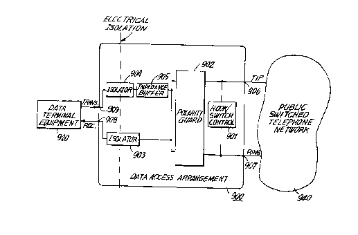
Figure 1 is a block diagram of a data access
arrangement (DAA) 900 coupled between a data terminal
equipment (DTE) 920 and the tip and ring lines of a
public switched telephone network (PSTN) 940. As
discussed above, the data access arrangement (DAA) soo
facilitates data communication between the data terminal
equipment (DTE) 920 and the public switched telephone
network (PSTN) 940.
CA 0222~733 1997-12-24
W O 97/02695 PCTnUS96/03489
The data access arrangement (DAA) 900 includes a
hook/switch controller 901, a polarity guard 902, a first
electrically isolating 903 coupler, a second electrically
isolating coupler 904, and an impedance buffer 905. The
hook switch controller 901 establishes DC continuity when
a call is in progress. That is, the hook switch
controller 901 establishes an "off hook" circuit. The
polarity guard 902 is typically a diode bridge and allows
the data access arrangement (DAA) 900 to function
properly regardless of the polarity of the voltage across
the tip and ring lines of the public switched telephone
network (PSTN) 940. The first and second electrically
isolating couplers 903 and 904, respectively,
~lectrically isolate the data terminal equipment (DTE)920
Erom the public switched telephone network (PSTN~ 940
while facilitating data transfer. As discussed above,
1the first and second electrically isolating couplers may
e~mploy a transformer, or optical isolators to provide the
required electrical isolation. The impedance buffer 905
:is used to provide a high input impedance and can be a
transistor, for example.
As shown in Figure 2, the DAA circuit of the present
~nvention includes an isolating controller 300, a first
phototransistor 500, a second phototransistor 600, a
iirst MOSFET 510, a second MOSFET 520, a third MOSFET 610
and a fourth MOSFET 620.
The first phototransistor 500 is optically
coupleable with a first LED 400. The first LED 400 emits
light when the data access arrangement (DAA) is to be
off-hook, i.e., when the data access arrangement (DAA) is
to be connected to the local telephone network. The data
access arrangement (DAA) is to be off-hook for example,
if a ring signal is detected on the tip or ring lines or
~ if the data terminal ec~uipment (DTE) requests connection
to the network (PSTN) for transmitting data. Similarly,
the second phototransistor 600 is optically coupleable
with a second LED 410. The second LED 410 emits light
CA 0222~733 1997-12-24
W O 97/02695 PCT/u~f5l~348g
when the DAA is to be off-hook. In an alternative
embodiment, the first and second LEDs 400 and 410,
respectively, can be replaced with a single LED which is
optically coupleable with both the first phototransistor
500 and the second phototransistor 600.
The collector of the first phototransistor 500 is
coupled with the tip line 100 of the public switched
telephone network (PSTN) and the source of the first
MOSFET 510, while the collector of the second
phototransistor 600 is coupled with the ring line 200 of
the public switched telephone network (PSTN) and the
source of the third MOSFET 610. The emitter of the first
phototransistor 500 is coupled with a first input
terminal 310 of the isolating controller 300 while the
emitter of the second phototransistor 600 is coupled with
a second input terminal 320 of the isolating controller
300.
A first output 330 of the isolating controller 300
is coupled to the gate of the first MOSFET 510 and a
second output 340 of the isolated controller 300 is
coupled with the gate of the second MOSFET 520. The
first and second outputs 330 and 340, respectively,
provide a high signal when a voltage is applied to the
first input 310. In an alternative embodiment, a single
output can replace the first and second outputs 330 and
340, respectively, because the first and second outputs
330 and 340, respectively, always provide the same
signal. Similarly, a third output 350 of the isolating
controller 300 is coupled with the gate of the third
MOSFET 610 and the fourth output 360 of the isolating
controller 300 is coupled with the gate of the fourth
MOSFET 620. The third and fourth outputs 350 and 360,
respectively, provide a high signal when a voltage is
applied to the second input 320. In an alternative
embodiment, a single output can replace the third and
fourth outputs 350 and 360, respectively, because the
CA 0222~733 1997-12-24
W O 97/02695 P~ '/03489
third and fourth outputs 350 and 360, respectively, will
always provide the same signal.
The drains of the first and third MOSFETs 510 and
610, respectively, are coupled together at a first node
561. The sources of the second and fourth MOSFETs 520
and 620, respectively, are coupled together at a second
node 562. The first node 561 is electrically coupled
with the second node 562 via the control block isolator
300.
Within the isolating controller 300, a first
electrical isolator (not shown), such as a transformer or
linear optocoupler for example, electrically isolates the
tip and ring lines from the transmit terminal 700 of the
~ata access arrangement (DAA). Similarly, also within
the isolating controller 300, a second electrical
isolator (not shown), such as a transformer or linear
optocoupler for example, electrically isolates the tip
and ring lines from the receive terminal 800 of the data
access arrangement (DAA).
In operation, when the data access arrangement (D~A)
wants to go "off hook", i.e., when the data access
~rrangement (DAA) wants to permit communication between
l:he data terminal equipment (DTE) and the public switched
1elephone network (PSTN), the first and second LEDs 400
and 410 are made to emit light. This can be in response
1:o the detection of a ring signal on either the tip line
or the ring line, or to a connection request from the
data terminal equipment (DTE) for transmitting data.
If the ring terminal 200 is supplied with a positive
voltage, this voltage is applied to the collector of the
~;econd phototransistor 600 and also to the source of the
t:hird MOSFET 610. The light emitted by the second LED
410 causes the second phototransistor 600 to conduct any
current due to the voltage from its collector to its
emitter (i.e., the second phototransistor is closed).
Since a voltage is applied to the second input 320 of the
isolating controller 300, a high signal is provided at
CA 0222~733 1997-12-24
W O 97/02695 PCTrUS96103489
the third and fourth output terminals 350 and 360,
respectively, of the isolating controller 300. Since
these high signals are applied to the gates of the third
and fourth MOSFETs 610 and 620, respectively, these
5 MOSFETs conduct (i.e., are closed). The voltage applied v
at the source of the third MOSFET 610 causes a current to
flow to the first node 561, which is coupled, via the
control block isolator 300 to the second node 562. The
second isolator (not shown) provides a representation of
10 the current caused by the voltage drop, to the receive
terminal 800. From the second node 562, the current
flows from the source to the drain of the fourth MOSFET
620, and thus, to the tip terminal 100.
Thus, by closing the third and fourth MOSFETs, 610
15 and 620, respectively, while the first and second
MOSFETs, 510 and 520, respectively, remain open, the
circuit functions as a polarity guard. The second LED
410 and the second phototransistor 600 switch the data
access arrangement (DAA) circuit to and from the public
20 switched telephone network (PSTN) while the first and
second isolators (not shown, which may be a transformer
or optocoupler, for example) of the control block
isolator 300 electrically isolate the data terminal
equipment (DTE) coupled with the DAA, from the public
25 switched telephone network (PSTN). Furthermore, the gate
of the third MOSFET 610 can be modulated with a
representation of a transmit signal from data terminal
equipment (DTE), provided by the first isolator. For
example, the third output 350 and the representation of
30 the transmit signal could be applied to two inputs of an
AND gate having an output coupled with the gate of the
third MOSFET 610. In this way, the same transistor
providing hook/switch control and facilitating polarity
guard functionality, can also be used to inject a
35 transmit signal onto the network (PSTN). Moreover, the
second phototransistor 600 will only sink a nominal
CA 0222~733 1997-12-24
W~D97/02695 PCT~S96/03489
11
voltage (as compared with 1.2 Volts sunk by the diode
bridge polarity guard) and has a linear characteristic.
If the tip terminal 100 is supplied with a positive
voltage, this voltage is applied to the collector of the
first phototransistor 500 and also to the source of the
first MOSFET 510. The light emitted by the first LED 400
causes the first phototransistor 500 to conduct any
current due to the voltage from its collector to its
emitter (i.e., the first phototransistor is closed).
Sillce a high input is applied to the first input 310 of
the isolating controller 300, a high signal is provided
at the first and second output terminals 330 and 340,
respectively, of the isolating controller 300. Since
these high signals are applied to the gates of the first
and second MOSFETs 510 and 520, respectively, these
MOSFETs conduct (i.e., are closed). The voltage applied
at the source of the first MOSFET 510 causes a current to
flow to the first node 561, which is coupled, via the
logic control block 300, to the second node 562. The
second isolator provides a representation of the current
caused by the voltage drop to the receive terminal 800.
The current at the second node 562 flows from the source
to the drain of the second MOSFET 520, and thus, to the
ring terminal 200.
Thus, by closing the first and second MOSFETs, 510
and 520, respectively, while the third and fourth
~OSFETs, 610 and 620, respectively, remain open, the
circuit functions as a polarity guard. The first LED 400
and the first phototransistor 500 switch the DAA circuit
to and from the local telephone network while the
transformers or optocouplers of the isolating
controller 300 electrically isolate a data terminal
equipment (DTE) coupled with the DAA, from the network
(PSTN). Furthermore, the gate of the first MOSFET 510
can be modulated with a representation of a transmit
signal from data terminal equipment (DTE), provided by
1he first isolator. For example, the first output 330
CA 0222~733 1997-12-24
W O 97/02695 PCT~US96/03489
12
and the representation of the transmit signal could be
applied to two inputs of an AND gate having an output
coupled with the gate of the first MOSFET 510. In this
way, the same transistor providing hook/switch control
and facilitating polarity guard functionality, can also
be used to inject a transmit signal onto the network
(PSTN). Moreover, the first phototransistor 500 will
only sink a nominal voltage (as compared with 1.2 Volts
sunk by the diode bridge polarity guard) and has a linear
characteristic.
The embodiments described herein are merely
illustrative of the principles of the present invention.
Various modifications may be made thereto by persons
ordinarily skilled in the art, without departing from the
scope or spirit of the invention.