Note : Les descriptions sont présentées dans la langue officielle dans laquelle elles ont été soumises.
CA 02226641 1998-O1-12
WO 97/03402 pCT/FI96~00407
1
Handling interrupts in a synchronous environment
The present invention relates to digital systems in
which a controller has to serve a plurality of peripheral
modules.
In digital systems, such as computers, peripheral
modules can ask for service from a central module, i.e. a
controller; by means of interrupts. In prior art systems,
for example in personal computers of industrial standards,
there is a dedicated interrupt line allocated to all
peripheral modules that are to be given the option to
request an interrupt. For example, said personal computers
have 15 interrupt lines. Although this is usually adequate
for PCs, in other kinds of environments, such as mobile
services switching centers and particularly transcoders
coupled to them, need often arises to serve even hundreds
of peripheral modules requesting an interrupt. To arrange
a separate interrupt line for such a large number of
peripheral modules would definitely be irrational.
A large number of peripheral modules are also
served in local area networks. In an Ethernet type of a
network, for example, a connecting cable has three states
used to identify the number of modules that have reserved
the cable: zero, one, or more than one. Most digital
circuits only handle two voltage states, which means that
carrying out a service request the way it is done in the
Ethernet network considerably increases the cost of the
apparatus. Another drawback of reserving turns in this
manner is that only a fraction of the connecting line
transfer capacity can in practice be utilized, because if
several modules ask for service at the same time, the
service requests of all the modules will be futile, with
the result that they all have to wait for a random time
before any new attempts.
It is possible to prevent an Ethernet type of
CA 02226641 1998-O1-12
WO 97/03402 PCT/FI96/00407
2
apparatus from becoming blocked in systems that are based
on reserving turns, for example in a Token Ring network in
which the turn circulates from one device to another in
the system. This arrangement, too, is expensive if applied
to a plurality of modules, because the logic that is used
to handle the interrupt turn must be installed in every
device.
A method for arranging an interrupt option for
several peripheral modules is proposed in the article
"Internal communications in a multiprocessor ISDN PBX",
Carlos Hirsch & Luis Rojas, Computer Communications, Vol.
18, Number 5, May 1995. In the system described in the
article, each peripheral module is allocated a pre-
determined time-slot during which it may request an
interrupt. As far as the connections between peripheral
modules are concerned, this system, too, is rather
burdensome to implement due to the handling of interrupts
requiring logZn lines if there are n peripheral modules.
It is an object of the present invention to solve
the aforementioned problems, and to offer an efficient and
easily applicable solution for distributing interrupt
turns to a large number of peripheral modules requesting
interrupts. This object is achieved with methods and
modules which are characterized by that which is claimed
in the independent claims.
From another point of view, the invention offers a
method and system by means of which a plurality of
peripheral modules can ask for service from a common
controller.
From a third point of view, the invention offers a
comprehensive solution to handshaking associated with
requesting and serving an interrupt.
The invention is based on preventing, in advance,
simultaneous interrupt requests from being produced by
giving each peripheral module that will possibly request
CA 02226641 1998-O1-12
WO 97/03402 PCT/FI96/00407
3
an interrupt a dedicated time-slot during which it is
allowed to request the interrupt. Each peripheral module
independently takes care that it will only request an
interrupt when permitted.
According to a further embodiment, in hierarchical
systems having peripheral modules with subperipheral
modules, the time slots can also be correspondingly
divided into sub-time slots.
In the following, the invention will be described
by means of preferred embodiments, with reference to the
attached drawings in which
Figure 1 is a chart illustrating an expected value
for delay as the number of peripheral modules increases,
Figure 2 illustrates coupling the system of the
invention to external circuits,
Figure 3 is a simplified block diagram of the
system according to the invention for handling interrupts
in digital signal processors,
Figure 4 illustrates the circuit of Figure 3
supplemented, and
Figure 5 illustrates applying the invention in a
general case.
Figure 1 is a chart illustrating an expected value
for delay as the number of peripheral modules increases.
Graph A shows the expected value for the delay in an
environment where the peripheral modules may interrupt at
a random moment in time. As the number n of the peripheral
modules increases, the exQected value for the delay
approaches infinity because an ever increasing amount of
time is wasted due to several peripheral modules asking
for service simultaneously, whereby the attempt will be
futile for all the modules. Graph B shows the expected
value for the delay in an environment where the peripheral
modules may only interrupt in their turn, and the
interrupt turn circulates via n peripheral modules in the
CA 02226641 1998-O1-12
WO 97/03402 PCT/FI96/00407
4
system. In this case, the expected value for the delay
increases linearly as the value of n increases. With low
values of n, the free interrupt alternative depicted by
graph A is better. With high values of n, the cyclic
interrupt turn depicted by graph B is better.
To better illuminate the invention, the embodiments
thereof are described in connection with a transcoder
coupled to mobile services switching centers, but it is
obvious that the invention is applicable to any
environment in which a controller has to serve a plurality
of interrupting peripheral modules.
Figure 2 illustrates signals employed by the
system. As far as the invention is concerned, the
essential parts in this exemplary block diagram are a
transcoder controller TRCO and 14 transcoder units TRO-
TR13, each unit having 16 digital signal processors DSPn.
Hence, there are 224 digital signal processors DSPn.
Naturally, it is possible to install a smaller number of
units in the system. The reason why there are 14
transcoder units is that one 64 kbps line can convey 14
calls coded in the half-rate of 6,5 kbps.
In this example, the interrupt sources, i.e.
peripheral modules possibly requesting an interrupt from
the controller TRCO, are said transcoder units TRO-TR13,
TRn in short. They request an interrupt with an INT'
signal. The controller TRCO indicates to begin serving the
interrupt with an interrupt acknowledgement signal INTA'.
Each unit TRn will have to request an interrupt whenever
any of its signal processors DSPn requires service.
Therefore, there are altogether 224 possible causes for an
interrupt.
The interrupt turns are coordinated by means of two
clock signals, CLK and SYNC, being present in the
exemplary apparatus for other purposes as well. As far as
the invention is concerned, they are used to make sure
CA 02226641 1998-O1-12
WO 97/03402 PCT/FI96/00407
that the interrupt sources have the same view of time. In
Figure 2, the signals CLK and SYNC are represented as
outputs from a clock generator CG. As far as the invention
is concerned, it is not significant whether the clock
5 generator CG is internal or external to the TRCO.
An interrupt source informs the identifiers of the
unit TRn that requested the interrupt and the signal
processor DSPn by using the data bus DATA. Like the clock
signal the data bus, too, has been installed in the system
for other uses as well, which means that the only signals
reserved for handling an interrupt are the interrupt
request signal INT' and the interrupt acknowledgement
signal INTA'.
The frequency of the CLK signal is the frequency of
the SYNC signal multiplied by a power of two, the power of
two at least equalling the number of interrupt sources. As
there may be 224 interrupt sources in the example, the
frequency of the clock signal must be at least 256 times
the frequency of the SYNC signal. By setting the ratio of
signals CLK and SYNC to be a power of two, the logic
associated with assigning interrupt turns can be
maintained as simple as possible. In the exemplary
apparatus, the SYNC signal has the frequency of 8 kHz and
the CLK the frequency of 8,192 MHz.
The period between SYNC pulses is divided into
equal intervals between the different interrupt sources.
The interrupt sources ask for an interrupt by the INT'
signal which each interrupt source may only activate in
its turn. Prior to activating the INT' signal, the
interrupt sources make sure that the INT' is not currently
active. Such a situation would indicate a fault in the
apparatus.
When the controller detects an active INT' signal,
it acknowledges the interrupt request by activating the
INTA' signal. Next, the interrupt source writes
CA 02226641 1998-O1-12
WO 97/03402 PCT/FI96/00407
6
information indicating the cause of the interrupt onto the
bus. According to the preferred embodiment, this
information consists of the identifier of the signal
processor requesting service and the identifier of the
transcoder unit within the signal processor. The
controller reads the interrupt source identifier from the
data bus and deactivates the INTA' signal. Following this,
the interrupt sequence can begin anew.
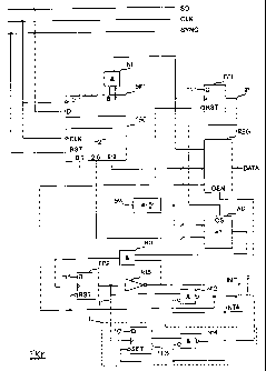
Figure 3 illustrates signals associated with an
interrupt by one of the transcoder units TRn in an
advantageous embodiment of the invention. The other
features of the unit TRn are not illustrated. The circuit
illustrated in Figure 3 functions as follows. At first, it
is assumed that block 1, demarcated by a broken line in
Figure 3, does not exist, and that the activation input
OEN of the register IREG input is applied from the gate
N12 output along line 2 denoted by a broken line. The
circuit monitors a serial mode time multiplexed line SD
(Serial Data?. The transcoder unit TRn requests an
interrupt when any of its signal processors DSPn (not
shown) requires service. In this case, the signal
indicating service requirement is not fed from the signal
processors DSPn but a simpler circuit will be obtained by
utilizing data on the time multiplexed bus SD. Due to time
multiplexing, one device is capable of detecting that any
of the signal processors DSPO-DSP15 requires service. This
is detected by an AND gate N1 coupled to the register SR1.
The reference mark of the register SR1 refers to a Shift
Register, but the register SR1 can be implemented in other
ways as well, for instance with successive flip-flops and
timing logic associated thereto. As far as the invention
is concerned, the essential matter is that the register
SR1 and the gate N1 will recognize a situation when an 8
bit byte having ones in the two most significant bits has
just been transferred on the bus, which in PCM signalling
CA 02226641 1998-O1-12
WO 97/03402 PCT/FI96/00407
7
indicates the last byte of a 4 byte frame. This
information is applied to flip-flop FF1 and an interrupt
register IREG. The output IF (Interrupt Flag) of flip-flop
FF1 acts as a chip select for an Address Decoder AD which
compares the output bits 2-5 of a Time Slot Counter TSC to
a reference address set by switches SW. Bits 0-1 from the
counter TSC are not fed anywhere in this particular
embodiment, but the counter TSC stages corresponding with
them divide the frequency of the CLK signal by four. The
switches SW may be located at each transcoder unit TRn or
in their rear wiring. In the latter case, the units TRn
may be identical. As the output bits 2-5 of the counter
TSC have 16 possible states and the switches SW are
positioned differently for each transcoder unit TRO-TR13,
the output of the address comparator AD can only be active
in one unit TRn at a time.
The output of the address comparator AD is
functionally applied to a flip-flop FF2. There is an AND
gate N11 between the aforementioned to make sure that no
interrupt will be requested if another unit TRn
simultaneously asks for an interrupt. In the circuit of
Figure 3, the signals INT' and INTA' are active in state
0. State 0 of the INT' signal would therefore block the
signal from the address comparator AD from reaching flip-
flop FF2. Unless the apparatus is faulty, need for service
can only exist in one transcoder unit TRn at a time,
whereby the INT' is in state "1" and the signal from the
address compar_ator is forwarded to flip-flop FF2 whose
output II (Internal Interrupt) is buffered by means of an
open collector type of buffer N13 to form an interrupt
request signal INT' for the controller TRCO. Signal II is
also fed via the AND gate N12 to the interrupt register
IREG. A condition to the active signal II passing gate N12
and consequently producing an active Output Enable (OEN)
signal to the interrupt register IREG is that INTA' signal
CA 02226641 1998-O1-12
WO 97!03402 PCT/FI96/00407
8
is active, i.e. 0. The active INTA' signal resets flip-
flops FF1 and FF2. When the OEN is active, the interrupt
register IREG inserts, onto the bus DATA, the identifier
of the transcoder unit TRn (from the switches SW? and the
identifier of the signal processor DSPn (output bits 6-9
of the counter TSC). Having read the bus DATA, the
controller TRCO deactivates the INTA' signal.
In the above configuration, the circuit of Figure 3
is not entirely adequate due to the output signals of the
register IREG being active for only a very short time.
They are deactivated when flip-flop FF2 is reset upon
reset of the INTA' signal. It is now assumed that the
conductor 2 does not exist, and block 1 has been
installed. At the rising edge of the FF2 output, the
output of FF3 also rises to "1". This signal is applied to
gate N14 to whose second input an inverted INTA' signal is
applied. Activation of the INTA' signal. activates the
output of gate N14, which in turn activates the outputs of
the register IREG. Deactivation of the INTA' signal
deactivates the output of gate N14, whereby the outputs of
the register IREG change into high impedance outputs. In
addition, the deactivation of the INTA' signal causes "0"
to be stored in flip-flop FF3.
As the INTA' signal is activated, the output of
flip-flop FF1 and the INT' signal are deactivated. As the
INTA' signal is deactivated, the outputs of the register
IREG change into high impedance outputs, and the interrupt
sequence terminates.
If the controller TRCO in the circuit of Figure 3
has no time to serve an interrupt from a transcoder unit
TRn before there is again need in the same unit TRn to
interrupt, the previous interrupt request of the unit will
be left without service. Figure 4 illustrates the circuit
of Figure 3 supplemented so that the need for an interrupt
will not be "forgotten" even if it cannot be attended to
CA 02226641 1998-O1-12
wo 9~io~oi rcTmoo4o~
9
immediately. Same reference marks denote common parts of
Figures 3 and 4. In the circuit according to Figure 4, the
output of AND gate N1 is applied to OR gate N2, to whose
second input is applied the output of a shift register
SR2. Output "1" of gate N2 indicates that a need exists of
an interrupt (as in the circuit of Figure 3) or that such
a need existed prior to the current moment in time, and
that this piece of information has now circulated via the
shift register SR2. The clock frequency of the register
SR2 will be obtained by dividing the frequency of the CLK
signal by eight by means of a divider D1. Thus, when the
register SR1 is stepped once for each bit of serial mode
data SD, the register SR2 is stepped once for each 8-bit
word of the serial mode data SD. The output of gate N2 is
applied to AND gates N3 and N4. The N3 output follows the
N2 output if the signal IF is "0", which means that no
previous interrupt sequence currently being dealt with
exists. The N4 output follows the N2 output if the signal
IF is "1", which means that an interrupt sequence
previously activated is currently in progress. In this
case, the need for an interrupt will be stored in shift
register SR2 until the signal processor in question is
next allowed to request an interrupt.
In the above, an embodiment of the invention has
been described in an environment where the clock signals
CLK and SYNC exist for other uses as well. If it desired
that the number of conductors required by the
synchronization signals be reduced, the signals can be
integrated in the same conductor for example so that the
pulses corresponding to the SYNC signal somehow, for
instance in length, differ from the pulses of the CLK
signal.
In circuits illustrated in Figures 3 and 4, the
need for an interrupt is not detected directly from the
signal processors, but gate N1 coupled to shift register
CA 02226641 1998-O1-12
WO 97103402 PCT/F196/00407
SR1 is used to identify that such a need exists. Figure 5
illustrates an embodiment of the invention in an apparatus
in which the need for an interrupt is recognized directly
from the peripheral modules. Block 1 demarcated by a
5 broken line was described in connection with Figure 3. In
the example, it is assumed that there are no more than 256
peripheral modules. An 8-bit counter TSC2 is synchronized
with the SYNC signal and it is stepped by a signal
256*SYNC having a frequency 256 times that of the SYNC
10 signal. Each possible peripheral module corresponds with
one value of counter TSC2. The peripheral module indicates
a need for an interrupt with a signal IC (Interrupt
Cause). It is assumed that no new pulses of the IC signal
arrive before the interrupt has been dealt with. A
positive IC signal pulse raises the output of flip-flop
FF A to "1" . This is applied to AND gate N21, the other
inputs of which are the interrupt request signal INT' and
the comparator AD2 output which is "1" if the TSC2 output
matches the reference address arranged in the comparator
AD2 by means of switches SW2. If all the gate N21 outputs
are true, its output is true, and state "1" will be stored
in flip-flop FF B. If the FF A output is "0", there is no
need for an interrupt, and nothing happens in the circuit
of Figure 5. If the FF A output is "1" and INT' signal is
"0", an other interrupt source has activated the INT'
signal. As a result, the gate N21 output will not be
activated and the interrupt source will wait for its turn
until the TSC2 output next matches the reference address
ADDR arranged in the comparator AD2.
At the rising edge of the FF B output, the address
ADDR of the interrupt source is stored in the register
IREG2. Instead of the ADDR, the TSC2 output could also be
used because a condition for storing in the register IREG2
is that the TSC2 output matches the ADDR.
The FF B output is applied to gate N22, to whose
CA 02226641 1998-O1-12
WO 97/03402 PCT/FI96/00407
11
second input is applied an interrupt acknowledgement
signal INTA' from the central equipment (not shown) . After
some time from the activation of the interrupt request
signal INT', the central equipment acknowledges the
interrupt by an INTA' signal which is in an inverted state
connected to gate N22. The N22 output thereby changes to
"0", which resets flip-flops FF A and FF B, and directs
the signals connected to the data bus of the register
IREG2 from high impedance state to active signals.
In the embodiment described above, each Peripheral
Module PM has been given a dedicated time slot for the
possible interrupt request, and each subperipheral module,
such as a signal processor, a dedicated signal IC by means
of which the subperipheral device can ask for an
interrupt. The invention can also be applied so that
specific bits of the time slot counter, for example the
four least significant bits, correspond with the time slot
assigned to each peripheral module, and the other bits,
the four most significant bits, correspond with the sub-
time slot assigned to each subperipheral module. There is
no separate figure illustrating this, but on the basis of
Figures 3-5 and the description related thereto this
solution is easy to comprehend at least by persons skilled
in the art.
The interrupt system according to the invention is
simple and economical to implement because it only
requires two signals, INT' and INTA', in addition to those
that- have to be installed in the apparatus anyway. The
system of the invention is also equitable; in the long run
the response time from the service request to carrying out
the service is equal in length for all the peripheral
modules. The third advantage of the interrupt system
according to the invention is that as there are no
simultaneous service requests, they can not cause down
time, either. Furthermore, the interrupt system of the
CA 02226641 1998-O1-12
wo 9~io3ao2 rcTmooao~
12
invention is fast due to the fact that finding out the
cause for the interrupt only requires one read transaction
from the bus.
In the description above, the service requests
targeted at the controller of the peripheral modules has
been referred to as "interrupt", which usually means that
after having received the service request the controller
interrupts its current task, serves the peripheral module
and continues the task that was interrupted. On the basis
of the description, it is obvious that the invention and
the different embodiments thereof are not dependent on how
the controller carries out the service. Hence, the
invention is applicable to handling any type of service
requests.
The invention has been described by way of example
in connection with transcoders connected to mobile
services switching centers. It is obvious to a person
skilled in the art that the basic idea of the invention
can be applied to many other environments as well. It is
particularly noteworthy that there are a variety of
different ways regarding the implementation of the need
for an interrupt and the clock signals CLK and SYNC.
Therefore, the invention is not restricted to the above
embodiments, but it may be applied widely without
departing from the scope and spirit of the attached
claims.
35