Note : Les descriptions sont présentées dans la langue officielle dans laquelle elles ont été soumises.
CA 02227102 1998-01-16
DEMODULATING APPARATUS
BACKGROUND OF THE INVENTION
Field of the Invention:
The present invention relates to a demodulating
apparatus for demodulating a modulated signal obtained by
m,odulating a plurality of carriers having different frequencies
by using data.
Description of the Related Art:
As a modulating apparatus for demodulating a
miodulated signal obtained by modulating a plurality of carriers
having different frequencies by using data, an apparatus for
demodulating an orthogonal frequency division multiplex (OFDM)
modulated signal (hereinafter referred to as an OFDM modulated
signal) employed in a digital audio broadcasting (DAB) or the
like carried out in Europe has been proposed.
In this OFDM modulation, data such as audio data or
the like are encoded by using a modulated signal using a large
number of carriers whose frequency components have orthogonal
relationships with one another, and the encoded data are
allocated to the respective carriers to thereby modulate the
respective carriers. Further, a digital signal in a frequency
domain fon~ed of the respective modulated carriers is converted
by inverse fast Fourier transform into a digital signal in a
time domain, and then the digital signal in the time domain is
converted into an analog signal. When the modulated signal is
demodulated, the OFDM modulated signal is converted into a
CA 02227102 1998-01-16
digital signal, and then the digital signal is subjected to fast
Fourier transform, thus the encoded data allocated to the
respective carriers being obtained.
In the OFDM modulation in the DAB, the respective
carriers are subjected to a quadrature phase shift keying (QPSK)
modulation by allocating one carrier to a two-bit data each.
Therefore, this modulation is referred to as OFDM-QPSK
modulation.
In the OFDM modulation, the point number of the fast
Fourier tr~nsform corresponds to the number of carriers.
According to a DAB standard, the point number is changed
depending upon modes. In modes 1, 2, 3, 4 thereof, the point
number is 1536, 384, 192, 768, respectively. Accordingly, if
the mode i, the mode 1, it is possible to transmit data of 2
(bits) x 1536 = 3072 (bits) by the OFDM modulation. This
transmission unit is called as a symbol. In the modes 1, 2 and
4, a group of seventy-six symbols is referred to as a frame, and
in the mode 3, a group of one hundred and fifty-three symbols is
referred to as a frame. Each of the above numbers of the
symbols in one frame does not includes the number of a null
symbol.
Synchronization is usually adjusted by adding several
synchronization symbols each formed of a synchronization
adjustment data to a head of one frame. According to the DAB
standard, of the seventy-seven symbols or one hundred and fifty-
four symbo:Ls (both of which include the null symbol and are
respective]Ly those in the modes 1, 2 and 4 and the mode 3), two
CA 02227102 1998-01-16
symbols including a null symbol are employed as the
synchronization symbol. A demodulation side (reception side)
compares amplitudes of a real-number portion and an imaginary-
number portion of the synchronization data subjected to the fast
Eourier transform with an previously held amplitude of the
normal synchronization data (i.e., an amplitude of a
synchronization data practically set by a transmission side) to
calculate a difference between synchronization phases upon fast
Fourier transform. Further, the demodulation side adjusts a
timing of the fast Fourier transform in response to the
synchronization phase difference to obtain synchronization. In
this method, since the synchronization can be obtained only once
in one frame, it disadvantageously takes a considerable time to
obtain syn~hronization.
A synchronization generating processing for
generating a synchronization signal on the demodulation side
(reception side) based on the signal obtained by converting the
OFDM modulated signal into an analog signal will be described.
The above symbol will be described with reference to FIG. 1.
The symbol is formed of a guard interval positioned on its head
side and an effective symbol positioned on its end side. The
effective symbol includes a period having correlation to the
guard interval, i.e., a period having the same signal portion
and the same interval on the end side thereof.
An original signal (e.g., a symbol of mode 1) shown
in FIG. 2A is delayed by a time corresponding to a an effective
symbol per:iod in the symbol. A signal of a period on the end
CA 02227102 1998-01-16
side of the original signal shown in FIG. 2A corresponding to
the guard interval (whose period is about 1/5 time as long as
the symbol period) and a signal of a guard interval of the
delayed signal shown in FIG. 2B are stored in a memory, and then
both of the signals stored in the memory are multiplied with
each other by using a digital signal processor (DSP) or the
like. A product of the multiplication is integrated by a low-
pass filter, thereby correlation being detected. Then, since
the signal on the end side of the effective symbol of the symbol
of the original signal which has the same interval and the same
signal portion as those of the guard interval and the signal of
the guard interval of the symbol of the delayed signal are the
same, i.e., have the same correlation with each other, a
correlation signal having a rectangular waveform (shown in FIG.
2C) is obt~ined.
If the correlation signal is subjected to interval
integration (moving average) using a width of time corresponding
to the guard interval in the symbol, then there can be obtained
as shown in FIG. 2D a signal which has an axially symmetric
triangular waveform and which starts being inclined upward at
the rising edge of the correlation signal indicative of
correlation and having a rectangular waveform and starts being
inclined downward at the trailing edge of the correlation
signal. As shown in FIG. 2D, the signal obtained by subjecting
the correlation signal to interval integration is compared with
a threshold level TH slightly lower than an amplitude level of
the practically obtained triangular wave signal, and thereby a
CA 02227102 1998-01-16
noise is removed therefrom to obtain only the normal signal
obtained by subjecting the correlation signal to interval
integraticn. A peak position of the signal obtained by
subjecting the correlation signal to interval integration is
discriminated, thereby a time synchronization signal
synchronized with the discriminated peak position being
generated.
A guard interval removal signal is generated based on
the time synchronization signal. The guard interval in the
signal obtained by converting the OFDM modulated signal into an
digital signal is removed by the guard interval removal signal
and then the timing of the fast Fourier transform is controlled
based on the time synchronization signal. The time
synchronization signal is also used when data of a signal
subjected to the fast Fourier transform is decoded.
A phase of the time synchronization signal is
discriminated. Based on the discrimination result, a frequency
synchronization signal is generated. The time synchronization
signal is converted into an analog signal, i.e., an auto
frequency control (AFC) signal (frequency control signal). An
oscillation frequency of a local oscillator for frequency
conversion is controlled based on the AFC signal. A RF
reception signal is thus frequency-converted into a signal
having an intermediate frequency, and then subjected to the
above A/D conversion.
At present, the known DAB signals are signals of
modes 1, 2, 3, 4. A determined basic period thereof is T t=l/
CA 02227102 1998-01-16
2048000 sec = 0.00048828 nsec). FIG. 3 shows a structure of the
~)AB signal of the mode 1, by way of example. In FIG. 3, the
basic period T and time are both indicated. One frame of the
ode 1 DAB signal is 196608 T (= 96 msec) and formed of one null
symbol (symbol number l=0) having an interval of 2656 T (= 1.297
msec) and seventy-six symbols (symbol numbers l = 1 to 76)
succeeding the null symbol and each having an interval of 2552 T
(= 1.246 msec).
Each of symbols having the symbol numbers l = 1 to 76
is formed of a guard interval having an interval of 504 T (=246
~sec) and an effective symbol at the succeeding position and
having an interval of 2048 T (+ 1 msec). Effective symbols of
the respective symbols having the symbol numbers l =1 to 76
include multicarriers of the number of k = 1536 having
frequencies different from one another. A carrier indicated by
0 is a carrier having a center frequency (a period of the
carrier is T). A carrier indicated by 1536/2 (=766) is a
carrier having a m~iml]m frequency, and a carrier indicated by -
1536/2 (=-766) is a carrier having a m;nimllm frequency. A data
amount of one symbol includes 1536 waves, and a data amount
thereof is 1536 x 2 bits, i.e, 48 capacity units (CU) x 64 bits.
The whole symbols having the symbol numbers l = 1 to
76 are referred to as an OFDM symbol.
In case of the mode 1, for example, the null symbol
having the symbol number l=0 and the symbol having the symbol
number l=l are referred to as time frequency and phase reference
(TFPR) symbols, respectively. A set of these two symbols is
CA 02227102 1998-01-16
referred to as a synchronization channel (sync. channel).
Symbols having the symbol numbers l=2 to 4 are referred to as
fast information channels (FIC). The whole FICs are divided
into twelve fast information blocks (FIB). The remaining
symbols having the symbol numbers l= 5 to 76 are classified into
four common interleaved frames (CIF).
An interval of each symbol of the DAM signal is
different depending upon the mode. An interval of each symbol
of the mode 2 is 1/4 time as long as the interval of each symbol
of the mode 1. An interval of each symbol of the mode 3 is 1/8
time as long as the interval of each symbol of the mode 1. An
interval of each symbol of the mode 4 is 1/2 time as long as the
interval of each symbol of the mode 1.
Specifically, in the mode 1, the interval of each of
the symbols excluding the null symbol is 2552 T (= 1.246 msec)
as described. In the mode 2, the interval of each of the
symbols ex,-luding the null symbol is 638 T (=2552T/4)(=312 ~sec
(= 1.246/4 msec)). In the mode 3, the interval of each of the
symbols excluding the null symbol is 319 T (=2552T/8)(=156 ~sec
(= 1.246/8 msec)). In the mode 4, the interval of each of the
symbols excluding the null symbol is 1276 T (=2552T/2)(=623 ~sec
(= 1.246/2 msec)).
In the mode 1, the interval of the effective symbol
in the sy~ol other than the null symbol is 2048 T (= 1 msec) as
described ~Ibove. In the mode 2, the interval of the effective
symbol in the symbol other than the null symbol is 512 T (= 2048
CA 02227102 1998-01-16
I'/4)(=250 ~lsec (= 1 msec /4)). In the mode 3, the interval of
the effective symbol in the symbol other than the null symbol is
256 T (= 2048 T/8)(=125 ~sec (= 1 msec /8)). In the mode 4, the
i.nterval of the effective symbol in the symbol other than the
null symbol is 1024 T (= 2048 T/2)(=500 ~sec (= 1 msec /2)).
Further, in the mode 1, the time of the guard
i.nterval in the symbol other than the null symbol is 504 T (=
246 ~sec). In the mode 2, the time of the guard interval in the
symbol other than the null symbol is 126 T (= 504 T/4) (= 61.5
~sec (= 246 ~sec/4)). In the mode 3, the time of the guard
i.nterval in the symbol other than the null symbol is 63 T (= 504
T/8) (= 30.75 ~sec (= 246 ~sec/8)). In the mode 4, the time of
the guard interval in the symbol other than the null symbol is
252 T (= 504 T/2) (= 123 ~sec (= 246 ~sec/2)).
In the above apparatus for demodulating the OFDM
modulated signal, when the synchronization signal is generated,
the original signal which is the OFDM modulated signal is
delayed by a time corresponding to the interval of the effective
symbol of the symbol. Further, the signals of the periods,
corresponding to the guard interval. of the original signal and
the delayed signal are stored in the memory. Then, both of the
signals stored in the memory are multiplied with each other and
then the product of the multiplication is integrated by the low-
pass filter, thereby the correlation being detected. The
CA 02227102 1998-01-16
correlation signal having the rectangular waveform and obtained
when the correlation is detected is subjected to interval
integration, thereby the signal having the triangular waveform
being obtained. The synchronization signal is generated by
discriminating a peak of the signal having the triangular
waveform. Therefore, if the TFPR symbol (second symbol) of each
frame is analyzed, then it is possible to shorten the time
required f~r obtaining synchronization as compared with a system
of establishing a frequency and time synchronization.
However, as the time of the guard interval is longer,
then number of multiplications for detecting correlation is
increased. This increase requires a lot of time and a larger
consumed power both for generation of the synchronization
signal. Moreover, this increase requires a memory of a large
capacity.
SUMMARY OF THE INVENTION
In view of such aspects, it is an object of the
present invention to provide a demodulating apparatus which
demodulates data by frequency-analyzing a time waveform of a
modulated signal that includes a plurality of carriers having
different frequencies modulated with data, is formed of a data
interval formed of one modulation time and a guard interval
accompanying the data interval and has an interval having
correlation with the guard interval at a position away from a
modulated signal by one modulation time, and which can provide a
shorter time required for generation of a synchronization
signal, a smaller consumed power required for generation of the
CA 02227102 1998-01-16
synchronization signal, and a memory of a smaller capacity.
According to an aspect of the invention, the
demodulating apparatus is one for demodulating a modulated
signal obtained by modulating a plurality of carriers having
different frequencies, and includes a data demodulating means
for demodulating data by frequency-analyzing a time waveform of
the modulated signal which is formed of a data period formed of
one modulation time and a guard interval succeeding the data
period and which includes in the data period a period having
correlation with the guard interval and provided at a position
away from the modulated signal by the one modulation time, a
correlation means for detecting correlation between the guard
interval of the modulated signal and the period in the data
period having correlation with the guard interval and provided
at a position away from the modulated signal by the one
modulation time, and a synchronization signal generating means
comprising the correlation means and for generating a
synchroniz,~tion signal based on a detection output from the
correlatio:n means. The correlation is detected in a
predetermi:ned period which is 1/2 as long as each of the guard
interval a:nd the period having correlation with the guard
interval and in which correlation can substantially be detected.
Therefore, since the correlation is detected in a
predetermined period which is 1/2 as long as each of the guard
interval and the period having correlation with the guard
interval and in which correlation can substantially be detected,
it is poss:ible to obtain a demodulating apparatus which can
CA 02227102 1998-01-16
provide a shorter time for generating the synchronization
signal, a smaller consumed power required for generating the
synchronization signal and a memory of a smaller capacity.
BRIEF DESCRIPTION OF THE DRAWINGS
FIG. 1 is a diagram showing a symbol;
FIGS. 2A to 2D are timing charts used to explain an
operation of a demodulating apparatus;
FIG. 3 is a diagram showing an frame structure of a
DAB signal of a model l;
FIG. 4 is a block diagram showing a transmitting
apparatus (modulating apparatus) according to an embodiment of
the present invention;
FIG. 5 is a block diagram showing a reception
apparatus (demodulating apparatus) according to an embodiment of
the present invention; and
FIGS. 6A to 6F are timing charts used to explain an
operation of the reception apparatus shown in FIG. 5.
DETAILED DESCRIPTION OF THE PREFERRED EMBODIMENT
A transmission apparatus according to an embodiment
of the present invention will hereinafter be described with
reference -to FIG. 4. A data generating circuit (encoder
circuit) 1 is supplied with audio data and other data (e.g, data
concerning a music, such as a title, a name of an artist, words
or the like, data of news, traffic information, still picture or
the like, ~nd so on) from input terminals 3, 4 and encodes the
supplied data to then supply the encoded data to an OFDM
modulator 2. The OFDM modulator 2 subjects the supplied
CA 02227102 1998-01-16
modulated signal to an orthogonal frequency division multiplex
processing to obtain an OFDM modulated signal, and then supplies
t.he OFDM m.odulated signal to a frequency converting circuit 23.
The frequency converting circuit 23 converts a frequency of the
OFDM modulated signal to obtain a high-frequency signal and then
supplies the high-frequency signal to a transmitting circuit 24.
The transm.itting circuit 24 carries out amplification of the
supplied high-frequency signal and so on and then transmits the
signal through an antenna 25 by wireless.
An arrangement of the data generating circuit 1 will
be described. An MPEG (moving picture experts group) encoder 5
is supplied with music data (audio data) from the input terminal
3 and compression-encodes the music data to supply the
compression-encoded music data to a transmission line encoder/
error correction code adder 6. The transmission line encoder/
error correction code adder 6 divides data of one symbol amount
into data groups each formed of adjacent two bits and allocates
carries having different frequencies to each of the data group,
then adding an error correction codes to the data thus encoded.
Then, the transmission line encoder/error correction code adder
6 supplies the encoded data to a time interleaving circuit 7.
The time interleaving circuit 7 interleaves the supplied encoded
data and then supplies the interleaved music data to a
multiplexing circuit 10.
A transmission line encoder/error correction code
adder 8 is supplied with other data (e.g, data concerning a
music, such as a title, a name of an artist, words or the like,
CA 02227102 1998-01-16
data of news, traffic information, still picture or the like,
and so on) from the input terminal 4. The transmission line
encoder/error correction code adder 8 divides data of one symbol
amount into data groups each formed of adjacent two bits and
allocates carries having different frequencies to each of the
data grou~s, then adding an error correction code to the data
thus encoded. Then, the transmission line encoder/error
correction code adder 8 supplies the encoded data to a time
interleaving circuit 9. The time interleaving circuit 9
interleaves the supplied encoded data and then supplies the
interleaved other data to a multiplexing circuit lO in which the
other data are multiplexed on the interleaved music data.
Under the control of a multiplexing control circuit
12, the multiplexing circuit 10 adjusts an order of the data in
a frequency domain in accordance with a frame arrangement of the
set mode. Under the control of the multiplexing control circuit
12, a fast information channel (FIC) generating circuit 13
adjusts an order of the data in a frequency domain in accordance
with a frame arrangement of the set mode. A frequency
interleaving circuit 11 is supplied with a multiplexed signal
from the multiplexing circuit 10 and an FIC signal from the FIC
generating circuit 13 and then frequency-interleaves both of the
supplied signals, and then supplies the frequency-interleaved
data to a sync. signal generating circuit 14. The sync. signal
generating circuit 14 adds a generated time-frequency-phase-
reference symbol (TFPR symbol) synchronization signal to the
supplied signal.
CA 02227102 1998-01-16
An arrangement of the OFDM modulator 2 will be
described. A serial/parallel converter 15 is supplied with a
frequency-interleaved output signal added with the TFPR symbol
synchronization signal and supplied from the synchronization
signal generating circuit 14 of the data generating circuit 1,
and then converts it into a parallel data to supply the parallel
data to an inverse fast Fourier transform circuit 16. The
inverse fast Fourier transform circuit 16 subjects the parallel
data to the inverse fast Fourier transform, i.e., sets a real~
number portion signal and an imaginary-number portion signal of
an output series formed of the respective carriers in response
to the par~llel data and then converts them into a real-number
portion signal and an imaginary-number portion signal of a time
series. The inverse fast Fourier transform circuit 16 supplies
the real-number portion signal and the imaginary-number portion
signal of the time series to a guard interval adding circuit 17.
The guard interval adding circuit 17 adds the guard interval
thereto, and then supplies the parallel data added with the
guard interval to a D/A converter 19 through a low-pass filter
20. The D/A converter converts the supplied parallel data into
an analog s,ignal, and then carries out an interpolation
processing.
An IQ modulating circuit 21 is supplied with the
real-nu3mbe;r portion signal and the imaginary-number portion
signal from the D/A converter 19, and then subjects them to
orthogonal modulation. The IQ modulating circuit 21 is supplied
with carriers having phases of 0~ and 90~ from a 0~/90~ carrier
14
CA 02227102 1998-01-16
generating circuit 22. A clock signal from a clock generating
circuit 18 is supplied to the inverse fast Fourier transform
circuit 16, the guard interval adding circuit 17 and the D/A
converter circuit 19.
The frequency converting circuit 23 is supplied with
the OFDM modulated signal from the IQ modulating circuit 21 and
then converts the OFDM modulated signal into a high-frequency
signal to supply it the transmitting circuit 24. The
transmitting circuit 24 carries out amplification of the high-
frequency signal and so on and transmits it through the
transmission antenna 25 by wireless.
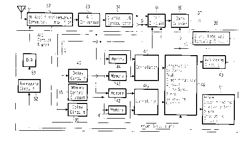
A reception apparatus according to the embodiment of
the present invention will be described with reference to FIG.
5. A high-frequency (RF) amplifier/frequency converter/an
intermediate-frequency (IF) amplifier 32 is supplied with a
received signal from an antenna 31 and then carries out
amplificat.ion of a high frequency, frequency conversion and
amplificat.ion of an intermediate frequency to thereby obtain a
OFDM modulated signal of a base band. The RF amplifier/
frequency converter/IF amplifier 32 supplies the OFDM modulated
signal to ~n A/D converter 33. The A/D converter 33 converts
the supplied OFDM modulated signal into a digital data and
supplies the digital data to a digital I/Q demodulator 34. The
digital I/(2 demodulator 34 demodulates the supplied OFDM
modulated signal to obtain a real-number portion data and a
imaginary-number portion data.
A fast Fourier transform circuit 35 is supplied with
CA 02227102 1998-01-16
the real-number portion data and the imaginary-number portion
data of the time series from the digital I/Q demodulator 34 and
then, after a guard interval removing circuit 50 of the
synchronization signal generating circuit 38 removes a guard
interval therefrom, converts them into the real-number portion
data and the imaginary-number portion data of the frequency
series. The fast Fourier transform circuit 35 supplies a real-
number por-tion data and the imaginary-number portion data of the
frequency series to a data decoder 36. The data decoder 36
decodes the supplied data to output the decoded data to an
output terminal 37. The data decoder 36 is formed of a
frequency deinterleaving circuit, a time deinterleaving circuit,
and an error correcting circuit which are successively connected
n serles.
An arrangement of the synchronization signal
generating circuit 38 of the reception apparatus will be
described. The real-number portion data and the imaginary-
number por~tion data from the digital IQ demodulator 34 are
supplied directly to memories 42, 44 of the synchronization
signal generating circuit 38 and also supplied through delay
circuits 3'3, 40 to memories 41, 43. FIG. 6A shows an original
signal formed of a real-number portion or an imaginary-number
portion, wherein reference letters Ta, Tb and Tc respectively
represent ~ symbol period, an effective symbol (data period in
one modula1ion time), and a guard interval. A period Tc
provided a1 the end of the effective symbol period Tb is a
period having correlation with the guard interval Tc. FIG. 6B
16
CA 02227102 1998-01-16
shows real-number portion data or imaginary-number portion data
delayed by the delay circuits 39, 40 by the effective symbol
period Tb.
Under the control of a memory control circuit 45,
only data (shown in FIGS. 6C, 6D) of a period which has a width
of Tc/4 or smaller on both sides relative to a center of the
data of the period having the correlation with the period Tc of
the original signal and the guard interval Tc, i.e., a total
width of Tc/2 or smaller and which is longer than a shortest
period where substantial correlation can be detected are written
in the memories 42, 44 and 41, 43. A correlator 46 detect~
correlation between the original signal of the I data and a
signal obtained by delaying the I data, and a correlator 47
detects correlation between the original signal of the Q data
and a signal obtained by delaying the Q data. When the
correlators 46, 47 detect correlation, both of the signals are
multiplied with each other by a DSP or the like. In this case,
the correlator 46 may detect the correlation between the
original signal of the I data and the delayed signal of the Q
data, and the correlator 47 detecting the correlation between
the original signal of the Q data and the delayed signal of the
I data. Alternatively, the correlator 46 may detect the
correlation between the original signal of the Q data and the
delayed signal of the I data, and the correlator 47 detecting
the correlltion between the original signal of the I data and
the delayed signal of the Q data.
The correlation signals having rectangular waveform
CA 02227102 1998-01-16
(shown in FIG. 6E) from the correlators 46 and 47 are supplied
to an integration-by-parts/peak discriminating circuit, i.e., a
time synchronization generating circuit 48, wherein a signal
obtained by subjecting correlation signal to interval
integration (as shown in FIG. 6F) (i.e., a signal which has an
axially symmetric triangular waveform and which is inclined
upward at a period of the correlation signal and inclined
downward after an end of the correlation signal period) being
obtained. The time synchronization signal generating circuit 48
is supplied with a rough synchronization signal from the RF
amplifier/frequency converter/IF amplifier 32. A level
comparing circuit is supplied with the signal obtained by
interval integration in order to remove a noise, and compares i~
with a threshold level TH slightly lower than an amplitude level
of the triangular wave signal. Thus, the level comparing
circuit removes the noise from the signal obtained by interval
integration to obtain a normal signal obtained by subjecting the
correlation signal to interval integration. A peak position of
the normal signal obtained by interval integration is
discriminated, thereby a time synchronization signal
synchronized with the peak position being generated.
As clear from FIG. 3 which shows a structure of the
DAB signal of the mode 1, the frame formed of seventy-six
continuous symbols (its number may be smaller, e.g., can be
fifty-five, thirty-five, fifteen or the like) excluding the null
symbol is successively transmitted. In this frame, the null
symbol, th~e synchronization symbol formed of TFPR symbols, and
18
CA 02227102 1998-01-16
the symbols including the actual data are provided in this order
from the head of the frame.
An averaging circuit 49 averages timings of the time
synchronization signals of the respective seventy-six symbols
(its number may be smaller, e.g., can be fifty-five, thirty-
five, fifteen or the like). Then, the averaging circuit 49
supplies the averaged time synchronization signal to the fast
Fourier transform circuit 35 to control the timing of the fast
Fourier transform, supplies the time synchronization signal to
the data decoder 36 to control synchronization of the respective
circuits of the data decoder 36, and supplies the time
synchronization signal to the guard interval removing circuit 5Q
to generate the guard interval removal signal.
The time synchronization signal generating circuit 48
also supplies the time synchronization signal to a phase
discriminating/frequency synchronization signal generating
circuit 51. The phase discriminating/frequency synchronization
signal generating circuit 51 generates a frequency
synchronization signal by discriminating a phase thereof and
supplies the frequency synchronization signal to an averaging
circuit 52. The averaging circuit 52 averages the frequency
synchroniz tion signals of the seventy-six symbols and supplies
the average frequency synchronization signal to a D/A converter
53. The D/A converter 543 converts the supplied average
frequency synchronization signal into an analog signal to obtain
an AFC signal, and then supplies the AFC signal to a local
oscillator of the frequency converter of the RF amplifier/
19
CA 02227102 1998-01-16
frequency converter/IF amplifier 32 to control an oscillation
frequency thereof.
~ hen a frequency deviation is 10 Hz, even if a period
during whi.ch data are written in the memories 42, 44 and 41, 43
is set shorter up to about Tc/16, it is possible to obtain the
high-accuracy synchronization signal.
According to a first aspect of the invention, the
demodulating apparatus for demodulating a modulated signal
obtained by modulating a plurality of carriers having different
frequencies by data includes a data demodulating means for
demodulating data by frequency-analyzing a time waveform of the
modulated signal which is formed of a data period formed of one
modulation time and a guard interval succeeding the data period
and which includes in the data period a period having
correlation with the guard interval and provided at a position
away from the modulated signal by the one modulation time, a
correlation means for detecting correlation between the guard
interval of the modulated signal and the period in the data
period having correlation with the guard interval and provided
at a position away from the modulated signal by the one
modulation time, and a synchronization signal generating means
comprising the correlation means and for generating a
synchronization signal based on a detection output from the
correlation means. The correlation is detected in a
predetermined period which is 1/2 as long as each of the guard
interval and the period having correlation with the guard
interval and in which correlation can substantially be detected.
CA 02227102 1998-01-16
Therefore, since the correlation is detected in a predetermined
period whi~h is 1/2 as long as each of the guard interval and
the period having correlation with the guard interval and in
which correlation can substantially be detected, it is possible
to obtain a demodulating apparatus which can provide a shorter
time for generating the synchronization signal, a smaller
consumed power required for generating the synchronization
signal and a memory of a smaller capacity.
According to a second aspect of the present
invention, the synchronization signal generating means comprises
a time synchronization signal generating means for subjecting
the detection output from the correlation means to interval
integration, discriminating a peak of a waveform subjected to
the interval integration, and generating a time synchronization
signal syn,-hronized with the peak, and a timing of frequency-
analyzing the time waveform of the modulated signal is
controlled based on the time synchronization signal from the
time synch:ronization signal generating means. Therefore, since
the correlation is detected in a predetermined period which is
1/2 as lonq as each of the guard interval and the period having
correlatio:n with the guard interval and in which correlation can
substantia:lly be detected, it is possible to obtain a
demodulating apparatus which can provide a shorter time for
generating the time synchronization signal used for controlling
the timing of frequency-analyzing the time waveform of the
modulated signal, a memory of a smaller capacity, and a smaller
consumed power required for generating the synchronization
CA 02227102 1998-01-16
signal.
According to a third aspect of the present invention,
the data of the modulated signal is an encoded data, the
demodulati.ng means comprises a decoding means for decoding the
frequency-analyzed output, and the decoding means is controlled
based on the time synchronization signal from the time
synchronization signal generating means. Therefore, it is
possible to obtain a demodulating apparatus which can provide a
shorter time for generating the time synchronization signal used
for controlling the timing of frequency-analyzing the time
waveform of the modulated signal and the timing of the decoder
means, a memory of a smaller capacity, and a smaller consumed
power required for generating the synchronization signal.
According to a fourth aspect of the present
invention, a demodulating apparatus further includes a frequency
converter means for frequency-converting a received signal to
obtain the modulated signal of a base band, the synchronization
signal generating means includes a frequency synchronization
signal generating means for discriminating a phase of the time
synchronizing signal from the time synchronization signal
generating means to thereby generate a frequency synchronization
signal, and an oscillation frequency of a local oscillation
means of the frequency converter means is controlled based on
the frequency synchronization signal from the frequency
synchronization signal generating means. Therefore, it is
possible to obtain a demodulating apparatus which can provide a
shorter time required for generating the time synchronization
CA 02227102 1998-01-16
signal use~ for controlling the timing of frequency-analyzing
the time waveform of the modulated signal and for generating the
frequency synchronization signal used for controlling the
oscillation frequency of the local oscillator means of the
frequency converter means, a memory of a smaller capacity, and
a smaller consumed power required for generating the
synchronization signal.
Having described a preferred embodiment of the
present invention with reference to the accompanying drawings,
it is to be understood that the present invention is not limited
to the above-mentioned embodiment and that various changes and
modifications can be effected therein by one skilled in the art
without departing from the spirit or scope of the present
invention as defined in the appended claims.
23