Note : Les descriptions sont présentées dans la langue officielle dans laquelle elles ont été soumises.
CA 02227150 1998-O1-15
APERTURE-COUPLED PLANAR INVERTED-F ANTENNA
Fie t he Invention
The present invention relates generally to antennas for use in cellular,
personal
communication services (PCS) and other wireless communication equipment and
more
particularly to a planar inverted-F antenna which utilizes aperture coupling
within the
antenna feed.
ac and of the Invention
Th.e continued growth in wireless communications is demanding personal base
stations, portable handsets and other communication terminals that are
compact, light
and able to perform a variety of functions. Considerable size reductions have
already
been achic;ved through the integration and miniaturization of most of the
electronic and
radio frequency (RF) circuitry in the communication terminal. However, the
conventional antennas typically used remain unduly large relative to the
terminal. This
is particularly true for designs which utilize multiple antennas in order to
provide
diversity, interference reduction and beamforming. A conventional antenna with
a low
profile structure suitable for mounting on personal base stations, portable
handsets and
other communication terminals is known as the planar inverted-F antenna
(PIFA).
FIG. 1 illustrates an exemplary PIFA 10 in accordance with the prior art. The
PIFA 10 includes a ground plane 12, an LPxWp rectangular radiating patch 14
and a
short-circuit plate 16 having a width d, which is narrower than the width Wp
of the
radiating patch 14. The short-circuit plate 16 shorts radiating patch 14 to
the ground
plane 12 along a null of the TM1~ dominant mode electric field of patch 14.
The PIFA
10 may thus be considered a rectangular microstrip antenna in which the length
of the
rectangular radiating patch 14 is reduced in half by the connection of the
short-circuit
plate 16 at the TM,~ dominant mode null. The short-circuit plate 16 supports
the
radiating patch 14 at a distance d2 above the ground plane 12. The radiating
patch 14
is fed by a TEM transmission line 18 from the back of the ground plane 12, at
a point
CA 02227150 1998-O1-15
2
located a distance d3 from the short-circuit plate 16. The transmission line
18 has a
width d4 and includes an inner conductor 20 surrounded by an outer conductor
22. A
detailed analysis of the operation of the conventional PIFA 10 of FIG. 1 may
be found
in K. Hirasawa and M. Haneishi, "Analysis, Design and Measurement of Small and
Low-Profile Antennas," Artech House, Norwood, MA, 1992, Ch. 5, pp. 161-180,
which is incorporated by reference herein. The PIFA 10 is particularly well-
suited for
use in personal base stations, handsets and other wireless communication
terminals
because it has a low profile, a large bandwidth and provides substantially
uniform
coverage, and because it can be implemented using an air dielectric as shown
in FIG. 1.
The bandvvidth of the PIFA 10 may be further increased by using a conducting
chassis
of a terminal housing as the ground plane 12. This is due to the fact that the
radiating
patch 14 will then have a size comparable to the ground plane and will
therefore induce
surface current on the ground plane.
A significant problem with antennas such as the conventional PIFA 10 of FIG. 1
is that the radiating patch is fed by the TEM transmission line 18 or a
similar structure
such as a coaxial line. This generally makes the PIFA more difficult to
manufacture, in
that the relative position and other characteristics of the feed must be
implemented with
a high degree of accuracy, and the outer and center conductors must be
properly
connected. Moreover, the cost of a TEM transmission line or coaxial line and
its
associated connector is excessive; and may be several times the cost of the
rest of the
antenna. In addition, the use of a TEM transmission line or a coaxial line
limits the
tuning flexibility of the antenna feed in that the characteristics of such
lines are not
easily adjusted during or after manufacture. A TEM transmission line or a
coaxial line
may also be relatively difficult to interconnect with related circuitry in a
personal base
station, portable handset or other communication terminal. These and other
factors
associated with the use of a TEM transmission line or coaxial line feed unduly
increase
the cost of the antenna, and prevent its use in many cost-sensitive
applications. It
would therefore be desirable if an alternative feed mechanism could be
developed such
that the low profile, large bandwidth and uniform coverage advantages of PIFAs
could
CA 02227150 2000-02-09
be provided in personal base stations, handsets and other communication
terminals without
the drawbacks associated with transmission line feeds such as that shown in
FIG. 1.
As is apparent from the above, a need exists for an improved PIFA which avoids
the
excessive cost of conventional transmission line or coaxial feeds, is simpler
to manufacture
and integrate with related terminal circuitry, and provides more tuning
flexibility, without
sacrificing the low profile, large bandwidth and uniform coverage advantages
typically
associated with PIFAs.
Summary of the Invention
The present invention provides an improved aperture-coupled planar inverted-F
antenna (PIFA) particularly well-suited for use in personal base stations,
portable handsets or
other terminals of cellular, personal communications service (PCS) and other
wireless
communication systems. A PIFA in accordance with the invention utilizes an
aperture-
coupled feed in place of the TEM transmission line or coaxial line feed
typically used in
conventional PIFAs.
In accordance with one aspect of the invention, an aperture-coupled PIFA is
provided
which includes a radiating patch arranged on one side of a ground plane and
separated
therefrom by a first dielectric. The first dielectric may be an air dielectric
or part of an
antenna substrate constructed of foam or another suitable dielectric material.
A shorting strip
connects a side of the radiating patch to the ground plane and may also
support the radiating
patch in an embodiment in which the first dielectric is an air dielectric. The
shorting strip
shorts the radiating patch at a point corresponding to a dominant mode null
such that the size
of the radiating patch may be reduced by a factor of two relative to the patch
size required
without the shorting strip. The shorting strip may be connected at any point
along a side of a
rectangular radiating patch. For example, the shorting strip may be connected
to an
approximate midpoint of the edge. A microstrip feedline is arranged on an
opposite side of
the ground plane and is separated therefrom by a second dielectric. The second
dielectric may
be part of a
CA 02227150 1998-O1-15
4
feedline substrate having an upper surface and a lower surface, with the
ground plane
adjacent tile upper surface and the feedline adjacent the lower surface. The
feedline
substrate may be formed using conventional printed wiring board materials, and
may be
part of a printed wiring board in a personal base station, handset or other
communication terminal incorporating the PIFA. Signals are coupled between the
radiating patch and the feedline via an aperture formed in the ground plane.
The PIFA
of the present invention thus avoids the excessive cost associated with
conventional
transmission line or coaxial line feeds. The PIFA of the present invention is
also
generally easier to manufacture than a conventional PIFA, in that there is no
need to
provide precise positioning and connections for the center and outer
conductors of a
TEM transmission line or coaxial line. Moreover, the use of aperture coupling
provides improved tenability in that adjustments may be made to antenna
parameters
such as the length and width of the feedline, the size and shape of the
aperture, the
position a:nd size of the shorting strip and the relative proximity of the
shorting strip
and aperture.
In accordance with another aspect of the invention, improved tenability may be
provided by utilizing a portion of the microstrip feedline as a tuning stub.
For example,
the feedline may be configured to have a total length of Lf + L~, where Lf is
the length
of a first portion of the feedline from an input of the feedline to the
aperture, and L~ is
the length of a remaining tuning stub portion of the feedline extending past
the
aperture. The impedance seen from the feedline referenced at the aperture may
be
characteri:aed as a series combination of an equivalent impedance Z
representing the
combined effect of the aperture and radiating patch, and an impedance of the
tuning
stub portion of the feedline. Impedance matching can then be provided by
selecting the
real part of the equivalent impedance Z as substantially equivalent to the
characteristic
impedance of the feedline, while selecting the impedance of the tuning stub
portion to
offset any imaginary part of the equivalent impedance Z. In an exemplary
embodiment, an impedance match providing a voltage standing wave ratio (VSWR)
of
2.0 or better is achieved over a bandwidth of about 200 MHZ at frequencies on
the
CA 02227150 1998-O1-15
S
order of 2 GHz.
The present invention thus provides a planar inverted-F antenna which avoids
the excessive cost of conventional TEM transmission line or coaxial feeds, and
exhibits
improved manufacturability, tuning flexibility and ease of integration
relative to planar
inverted-F~ antennas with conventional feeds. Moreover, these improvements are
provided without sacrificing the low profile, large bandwidth and uniform
coverage
features typically associated with planar inverted-F antennas. These and other
features
and advantages of the present invention will become more apparent from the
accompanying drawings and the following detailed description.
Brie De cription of the Drawings
FIn. 1 shows a planar inverted-F antenna (PIFA) in accordance with the prior
art.
FIG. 2 shows an exploded view of an aperture-coupled PIFA in accordance
with an exemplary embodiment of the present invention.
FIG. 3 is an equivalent circuit illustrating tuning features of the aperture-
coupled P>FA of FIG. 2.
FIG. 4 is a Smith chart plot illustrating the input impedance of an exemplary
implementation of the aperture-coupled PIFA of FIG. 2 as a function of
frequency.
FIGS. 5 and 6 are far-field plots of respective E and H planes illustrating
the
uniform coverage provided by the exemplary aperture-coupled PIFA of FIG. 2.
D tailed Description of the Invention
The present invention will be illustrated below in conjunction with an
exemplary
aperture-coupled planar inverted-F antenna (PIFA). It should be understood,
however,
that the invention is not limited to use with any particular PIFA
configuration, but is
instead more generally applicable to any PIFA in which it is desirable to
provide
improved manufacturability, tunability or ease of integration without
undermining the
low profile, large bandwidth and uniform coverage advantages of the antenna.
The
CA 02227150 1998-O1-15
6
term "PIF'A" as used herein is thus intended to include not only the
illustrative
configurations, but also any antenna having a radiating patch suspended above
a
ground plane and shorted to the ground plane in at least one location. The
term
"aperture" as used herein in the context of aperture coupling is intended to
include not
only the illustrative rectangular apertures of the exemplary embodiments, but
also
apertures having a variety of other shapes and sizes. The term "shorting
strip" as used
herein is intended to include a metallic strip, plate, pin, lead or trace as
well as any
other conductive interconnect used to short a radiating patch to a ground
plane. For
example, a shorting strip in an aperture-coupled PIFA of the present invention
may be
implemented in the form of a short-circuit plate such as plate 16 shown in
FIG. 1. It
should be noted that the term "coupling" as used herein is intended to include
the
coupling of transmit signals from the feedline to the radiating patch of a
PIFA as well
as the coupling of received signals from the radiating patch to the feedline.
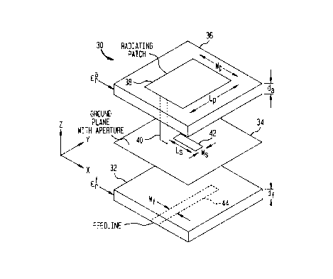
FIG. 2 shows an exploded view of an aperture-coupled PIFA 30 in accordance
with an e~;emplary embodiment of the present invention. The PIFA 30 includes a
feedline substrate 32, a ground plane 34 and an antenna substrate 36. The
antenna
substrate 36 in this embodiment will be assumed to represent an air dielectric
having a
thickness d~, but in alternative embodiments the antenna substrate 36 may be
formed
using other materials, such as foam, having a dielectric constant era. A
rectangular
radiating patch 38 having a width WP and a length Lp is formed in a plane
corresponding to an upper surface of the substrate 36. Although the patch
length Lp is
shown as greater than the patch width Wp in the illustrative embodiment of
FIG. 2, this
is not a requirement of the invention. The radiating patch 38 is shorted to
the ground
plane 34 by a narrow metallic strip 40 connected to one side of the patch 38
as shown.
The metallic strip 40 may also serve to support the radiating patch 38 in an
embodiment in which the substrate 36 represents an air dielectric. In
embodiments in
which the substrate 36 is formed of foam or other material, the substrate 36
may
provide complete or partial support for the radiating patch 38. The metallic
strip 40 is
connected. at approximately the midpoint of a side of the rectangular
radiating patch 38
CA 02227150 1998-O1-15
in the exemplary embodiment of FIG. 2. This arrangement provides a short-
circuit
rectangular microstrip antenna that resonates near the frequency of a patch of
length
2Lp, and thus allows the size of the radiating patch 38 to be reduced by a
factor of two
relative to the patch size required without the shorting strip. It should be
noted that the
dimensions of the various elements of PIFA 30 are not drawn to scale, and the
relative
dimensions shown in this illustrative example should not be construed as
limiting the
invention to any particular embodiment or group of embodiments.
The ground plane 34 includes a rectangular slot or aperture 42 having a length
LS and a width W5. The ground plane is supported in this embodiment by the
feedline
substrate 32 which may be formed of dielectric materials such as those
utilized in
conventional printed wiring boards. The feedline substrate 32 has a dielectric
constant
e~f and a thickness df, and may be part of an existing substrate layer of a
printed wiring
board in a personal base station, portable handset or other communications
terminal. A
microstrip feedline 44 having a width Wf is formed on a lower surface of the
feedline
substrate 32. The feedline 44 has a total length Lf + L~ which extends beyond
the
aperture 42. The initial portion of the feedline 44 up to the aperture 42 has
length Lf,
while the portion of the feedline 44 extending beyond the aperture 42 has
length L~ and
is used as .a tuning stub to provide improved tunability in a manner to be
described in
greater detail below.
In 'the PIFA 30 of FIG. 2,'the radiating patch 38 is fed electromagnetically
via
the combination of the feedline 44 and the aperture 42 rather than via a TEM
transmission line or coaxial line as in a conventional PIFA. The PIFA 30
therefore
avoids the excessive cost associated with the TEM transmission line or coaxial
line
feeds. The; PIFA 30 is also generally easier to manufacture than a
conventional PIFA,
in that there is no need to provide precise positioning and connections for
the center
and outer conductors of the TEM transmission line or coaxial line. Moreover,
the use
of the feedline 44 provides improved tunability in that adjustments may be
made in
PIFA 30 to antenna parameters such as the length of the feedline 44, the size
and shape
of the aperture 42, and the relative proximity of the shorting strip 40 and
aperture 42.
CA 02227150 1998-O1-15
8
These and other similar adjustments are not possible in the conventional PIFA
10
described in conjunction with FIG. 1 above. It will be shown in conjunction
with
FIGS. 4, 5 and 6 below that these improvements are provided without
undermining the
large bandwidth and substantially uniform coverage attributes commonly
associated
with PIFA.s.
FIG. 3 is an equivalent circuit illustrating tuning features of the aperture-
coupled Pl(FA of FIG. 2. The portion of the feedline 44 beyond the aperture 42
is
terminated in an open circuit and acts as a tuning stub having a variable
length L~ and a
characteristic impedance Z~. The initial portion of the feedline 44 up to the
aperture 42
has length Lf and characteristic impedance Z~. The combined effect of the
aperture 42
and the radiating path 38 is seen by the feedline 44 referenced at the
aperture 42 as an
equivalent impedance Z in series with the tuning stub portion of feedline 44.
Impedance; matching is achieved in the equivalent circuit of FIG. 3 when the
real part of
the equivalent impedance Z is substantially equal to the characteristic
impedance Z~ of
the feedline 44, while any imaginary part of the equivalent impedance Z is
substantially
canceled out by the tuning stub portion of the feedline 44. It will be shown
below that
this impedance matching condition can be achieved over a relatively large
bandwidth.
FIG. 4 is a Smith chart plot illustrating the input impedance of an exemplary
implementation of the aperture-coupled PIFA 30 of FIG. 2 as a function of
frequency.
The Smith chart plots the input impedance of the feedline 44 for frequencies
in the
range between about 1.9 GHz and 2.3 GHz. In generating the impedance
measurements of FIG. 4, the PIFA 30 of FIG. 2 was assumed to be configured
with a
radiating patch 38 having a length Lp of about 27.5 mm and a width Wp of about
50.0
mm. It wa.s also assumed that the ground plane 34 was an infinite ground
plane. The
radiating patch 38 was separated from the ground plane 34 by an air dielectric
or low
dielectric foam antenna substrate 36 having a thickness da of about 10 mm. A
shorting
strip 40 having a width of about 1 mm was used to short the radiating patch 38
to the
ground plane 34. The shorting strip 40 was connected to the approximate
midpoint of
the 50.0 mm side of the rectangular radiating patch in a manner similar to
that shown in
CA 02227150 1998-O1-15
9
FIG. 2. 'the aperture 42 of ground plane 34 was configured with a length LS of
about
55 mm and a width WS of about 2 mm. The center of the aperture 42 was
symmetrically placed with respect to the radiating patch 38 above it and its
distance
from the shorting strip 40 was set to about 2 mm. The ground plane 34 was in
contact
with the upper surface of the feedline substrate 32. The feedline substrate 32
had a
thickness df of about 0.5 mm and a dielectric constant e~f of about 3.8. The
microstrip
feedline 44 on the lower surface of the feedline substrate 32 had a width Wf
of about 1
mm and a total length Lf+ Lt of approximately 30 mm. The length L~ of the
tuning stub
portion of the feedline 44 was selected to be about 2.5 mm.
The Smith chart plot of FIG. 4 shows the variation of input impedance of
feedline 44 from a start frequency of about 1.9 GHz corresponding to point P 1
to a
stop frequency of about 2.3 GHz corresponding to point P4. The circle 50
represents a
constant voltage standing wave ratio (VSWR) circle. All impedance points in
the
Smith chart plot falling on or within the constant VSWR circle will provide a
VSWR of
2.0 or less at the input of the feedline 44. A VSWR of 2.0 corresponds to an
input S 11
value of about -10 dB, indicating that a reflection of an input signal applied
to the
feedline 44 will have a power level about 10 dB below that of the input signal
itself. In
a PIFA configured with the above-described exemplary parameters, the input
impedance at the start frequency of 1.9 GHz, corresponding to point P 1 on the
Smith
chart, creates a substantial impedance mismatch along the feedline 44 and thus
high
VSWR and S 11 values. As the operating frequency is increased, the input
impedance
curve enters the constant VSWR circle 50 at a point P2 which corresponds to a
frequency of about 2.09 GHz. The point P2 falls on the constant VSWR circle 50
and
thus has a VSWR of 2.0 and an S11 value of about -10 dB. The remaining
frequencies
up to 2.3 (sHZ are all within the constant VSWR circle 50 and therefore all
result in a
VSWR of less than 2.0 and S 11 values of better than -10 dB. The point P3
falls near a
zero reactance line on the Smith chart and corresponds to a frequency of about
2.2
GHz. As noted above, the point P4 corresponds to the stop frequency 2.3 GHz of
the
plotted input impedance curve. The input impedance plot of FIG. 4 indicates
that the
-,,.
CA 02227150 1998-O1-15
feedline 44, aperture 42 and radiating patch 38 can be well-matched over a
relatively
large bandwidth. For example, a PIFA configured with the exemplary parameters
given
above can provide an input VSWR of 2.0 or better over a bandwidth of more than
200
MHz.
5 FIGS. 5 and 6 show computed far-field plots for the respective E and H
planes
illustrating the coverage provided by the aperture-coupled PIFA 30 of FIG. 2.
The
PIFA 30 was assumed to be configured with the same exemplary parameters
described
above in conjunction with FIG. 4. The E plane plot of FIG. 5 shows a total
field ET, a
co-polar component Ee and a cross-polar component E~ for a ~ value of
90°. The
10 total field ET is equivalent to the co-polar component Ee in the FIG. 5
plot. The H
plane plol: of FIG. 6 shows a total field Er, a co-polar component E~ and a
cross-polar
component Ee for a ~ value of 0°. The plots indicate field strength as
a function of
direction around a point at the center of each plot. Each of the plots
includes five
concentric: circles surrounding the center point, with each concentric circle
corresponding to an additional increase of approximately 20 dB in field
strength
relative to the field strength at the center point. The fifth and outermost
concentric
circle ma~~ thus be considered a 0 dB circle, with the fourth, third, second
and first
concentric circles corresponding to relative field strengths of.-20 dB, -40
dB, -60 dB
and -80 d:B, respectively, and the center point corresponding to a relative
field strength
of -100 d13. The fields are plotted over a full 360° around the center
point. It can be
seen that the PIFA 30 of FIG. 2 provides a substantially uniform coverage over
the full
360° with a directivity comparable to that provided by much larger
dipole antennas.
The E and H plane plots of FIGS. 5 and 6 exhibit maxima around the 90°
and 270°
points, and sharp minima at the 90° and 270° points. The sharp
minima are
attributable to the above-noted assumption of an infinite ground plane. The
presence
of the shorting strip 40 in the PIFA 30 of FIG. 2 results in cross-polar
components
having a slightly higher level than those of a conventional aperture-coupled
microstrip
patch antenna. However, this feature may improve the antenna performance in a
multipath environment such as the interior of a building where there is a
strong
CA 02227150 1998-O1-15
11
presence of cross-polar components and a fixed antenna orientation is not
required. It
should be noted that the position of the shorting strip 40 relative to the
radiating patch
38 may be; used as a mechanism for adjusting the far-field performance of the
PIFA 30.
For example, although the shorting strip 40 is connected to patch 38 near the
midpoint
of the side; in the illustrative embodiments described above, the shorting
strip position
could be moved closer to a corner of the side of patch 38 in order to alter
the cross-
polar components, the position of the maxima and thus the directivity of the
far-field
radiation plot. The shorting strip 40 could thus be moved, for example, about
10 mm
from the midpoint of a side toward a corner of the radiating patch 38 in order
to
redirect th:e maxima toward the 0° angle in the plots of FIGS. 5 and 6.
The position of
the shorting strip 40 may also be varied to adjust impedance matching
conditions.
The present invention utilizes aperture coupling in a PIFA in order to avoid
the
excessive cost of conventional TEM transmission line or coaxial feeds, and to
improve
manufacturability, tenability and ease of integration relative to PIFAs which
utilize
1 S conventional TEM transmission line or coaxial line feeds. The resulting
aperture-
coupled P.IFA is particularly well-suited for use as a replacement for
existing extension
antennas in wall-mounted or desktop personal base stations, portable handsets
and
other types of wireless communication terminals. The aperture-coupled PIFA of
the
present invention provides a low profile, a large operating bandwidth and
substantially
uniform coverage in a multipath environment; with a gain and directivity
comparable to
that provided by much larger dipole antennas.
The above-described embodiments of the invention are intended to be
illustrative; only. Alternative embodiments may be implemented by altering the
size and
shape of the radiating patch 38, the size and shape of the aperture 42, the
size, shape
and relative position of the shorting strip 40 and the characteristics of the
feedline 44.
For example, although the feedline 44 is shown as having a constant width in
the
embodiment of FIG. 2, it should be apparent that application of conventional
impedance: matching techniques to the feedline may produce a non-uniform
width.
Such techniques may involve providing an impedance matching transformer at the
input
CA 02227150 1998-O1-15
12
of the feedline in the form of a length of transmission line having a larger
or smaller
width than the remaining portion of the feedline. Numerous other alternative
embodiments may be devised by those skilled in the art without departing from
the
scope of the following claims.