Note : Les descriptions sont présentées dans la langue officielle dans laquelle elles ont été soumises.
CA 02228781 1998-02-OS
- 1 -
BACKGROUND OF THE INVENTION
The present invention relates to a waveguide type
optical switch that is employed in the field of optical
communication, and more particularly to a waveguide type
optical switch which is small in size and suitable for
remote control.
Among conventional waveguide type optical
switches is a 1 X 2 optical switch disclosed in Japanese
Patent Unexamined Publication No. 6-148536. This 1 x 2
optical switch has a cantilever beam formed on a silicon
substrate, and serves to perform optical path switching by
moving an optical waveguide formed on the cantilever beam
with the use of electrostatic force.
In the aforementioned optical switch the follow-
ing points have not been taken into consideration.
First, the use of electrostatic force requires
the drive volt is as high as tens of volts or more, and a
single-cantilever beam structure for the optical switch
involves turning of a tip end of the waveguide concurrently
with translating motion at the time of optical switching
operation, which causes non-parallelism of the optical
entran~~e plane and optical exit plane of the waveguide,
leading to an increased loss of insertion. In addition, a
substrate is formed of silicon, and so if silica glass is
used as a material for the optical waveguide, the waveguide
CA 02228781 1998-02-OS
- 2 -
will be distorted or cracked due to a difference between
the linear expansion coefficients of the both components.
SUMMAF;Y OF THE INVENTION
It is an object of the present invention to solve
the above problems and provide a waveguide type optical
switch. which can be driven with a voltage of 10 volts or
less a.nd which is small in insertion loss and low in cost.
To achieve this end, an optical waveguide switch
according to the present invention comprises a silica glass
substrate; a plurality of cantilever beams formed in
parallel to one another on the silica glass substrate, and
connected at their tip ends to a connection member; at
least one input silica glass optical waveguide core formed
on the cantilever beams; a plurality of output optical
waveguide cores fixed in opposition to the input silica
glass optical waveguide core; and switch drive means for
bending the cantilever beams.
Further, the invention provides an optical switch
for switching an optical path of an input optical signal,
comprising a silica glass substrate, a separation layer
formed on the silica glass substrate, a plurality of
cantilever beams formed in parallel to one another on the
separation layer, and connected at their tip ends to a
connection member, at least one input silica glass optical
2.5 waveguide core formed on the cantilever beams, a plurality
of output optical waveguide cores fixed in opposition to
the input silica glass optical waveguide core, and switch
CA 02228781 1998-02-OS
- 3 -
drive means for bending the cantilever beams.
The thickness of the separation layer is less
than a height of the input optical waveguide core, and at
least one of the connection member or those members on the
substrate which are disposed to be brought into contact
with t:he connection member when an optical-path switching
operation is performed are recessed in a movement direction
of they connection member.
The switch drive means comprises soft magnetic
bodies provided on the connection member for the cantilever
beams and on the substrate, and an electromagnetic actuator
comprising a soft magnetic yoke provided on the substrate
and formed of a soft magnetic body, a permanent magnet, and
a wire coil.
The soft magnetic yoke is divided to form an
interior yoke formed of a soft magnetic body, and an
exterior yoke formed of a soft magnetic body and opposed to
the interior yoke through a cover formed with an insertion
hole for an index regulating liquid.
With the above arrangement, a plurality of
cantilever beams formed in parallel to one another and
connected at their tip ends to the connection member
function to have their tip ends moved parallel with one
another when an optical-path switching operation is
performed.
Therefore, the tip end portions of the optical
waveguides formed on the cantilever beams are also moved
parallel with one another upon the optical-path switching
CA 02228781 1998-02-OS
- 4 -
operation. This parallel movement of the optical wave-
guidea makes selection of an output optical waveguide to
enable optical path switching.
In the present invention, the silica glass
optical waveguides are formed on a silica glass substrate,
which can make the difference in liner expansion coeffi-
cient between the substrate and the optical waveguide layer
extremely small, and consequently it is possible to
suppress warp and deformation of the substrate and
cantilever beams to accurately position the optical wave-
guides on the emergent and incident sides.
In the present invention, the separation layer
provided on the whole or part of the silica glass substrate
is removed by etching, and so movable cantilever beams
separated from the substrate can be obtained with ease and
in a short time.
In the present invention, a press member fixed to
the substrate crosses at least one of the tip ends of the
cantilever beams, and so there is no possibility that the
cantilever beams will be separated from the substrate in a
vertical direction.
In the present invention, the cover for covering
the whole of cantilever beams allows an index regulating
liquid to fill around the cantilever beams and their
vicinities and eliminates the possibility of adherence of
foreign matters which may hinder a switching operation, and
so high reliable switching can be performed.
In the present invention, the thickness of the
CA 02228781 1998-02-OS
- 5 -
separation layer is less than the height of the optical
wavegu:ide, and so even if there were any positional
discrepancy equivalent to the gap between the silica glass
substrate and the cantilever beam after removal of the
separation layer, there would be no possibility that the
ends of the facing optical waveguides were completely
displaced from each other and therefore the optical coupl-
ing would be maintained. Accordingly, even in the case
where the cantilever beam is displaced by external
disturbance, an extreme reduction in the optical coupling
efficiency can be suppressed.
In the present invention, at least one of the
connection member or those members on the substrate which
are disposed to be brought into contact with the connection
member when an optical-path switching operation is
performed are recessed in a movement direction of the
connection member to thereby limit the contact area to a
small magnitude. Furthermore, it is possible to suppress
the index regulating liquid from entering portions, with
which the connection member and the aforementioned member
on the substrate contact, to form a gap therebetween.
In the present invention, magnetic forces are
generated between the soft magnetic body formed on the
connection member for cantilever beams and above the
substrate, and wire coils and the permanent magnet, and can
be utilized to deform the cantilever beam to thereby switch
the optical waveguide formed on the cantilever beam.
Further, in the present invention, the soft
CA 02228781 1998-02-OS
- 6 -
magnetic yoke formed of a soft magnetic body and constitut-
ing a part of a magnetic circuit can be divided to provide
an interior yoke formed of a soft magnetic body and
provided on the substrate, and an exterior yoke formed of a
soft magnetic body and opposed to the interior yoke with
the cover therebetween, so that it is possible to form only
the interior yoke inside the cover enclosing the entire
cantilever beam and the exterior yoke outside the cover.
With this arrangement, the wire coil and the permanent
magnet. are not received within the cover, so the cover can
be redluced in size and also foreign matters possibly
produced from the permanent magnet and the wire coil can be
prevented from adhering to the cantilever beam and their
vicinities.
Further objects and advantages of the present
invention will become apparent from the following detailed
description when read in conjunction with the accompanying
drawings.
BRIEF DESCRIPTION OF THE DRAWINGS
Fig. 1 is a fragmentary perspective view showing
an embodiment of a waveguide type 2-circuit 1 X 2 optical
switch according to the present invention;
Fig. 2 is a sectional view showing an actuator
for driving the waveguide type 2-circuit 1 X 2 optical
switch according to the present invention;
Fig. 3 is a plan view showing a second embodiment
of a waveguide type 2-circuit 1 x 2 optical switch
CA 02228781 1998-02-OS
according to the present invention;
Fig. 4 is a schematic, cross sectional view
showing a process, in which a cantilever beam is separated
from a. silica glass substrate;
Fig. 5 is a fragmentary perspective view of a
third embodiment of a waveguide type 2-circuit 1 x 2
optical switch according to the present invention;
Fig. 6 is a cross sectional view of the waveguide
type 2-circuit 1 x 2 optical switch shown in Fig. 2;
Fig. 7 is a fragmentary perspective view showing
an optical switch enclosed in a package;
Fig. 8 is a plan view showing an embodiment, in
which the waveguide type optical switch according to the
present invention is applied to a 2 X 2 optical switch;
Fig. 9 is a diagram showing the relationship
between the switched state of the 2 x 2 optical switch
shown in Fig. 8 and the light coupled state; and
Fig. 10 is a block diagram showing an embodiment
in which the waveguide type optical switch according to the
present invention is applied to an optical communication
equipment.
DESCRIPTION OF THE PREFERRED EMBODIMENTS
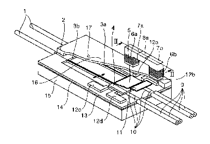
Referring to Fig. 1, there is shown a fragmentary
sectional perspective view of an embodiment of a waveguide
type 2-circuit 1 x 2 optical switch according to the
present invention. In this embodiment a silica glass
waveguide layer 13 is formed on a silica glass substrate 15
CA 02228781 1998-02-OS
$ _
through a separation layer 14. Movable optical waveguides
2 are formed on cantilever beams 3a and 3b, respectively.
Formed on the free end sides of the cantilever beams 3a and
3b is a connection member 4, and formed on the upper
surface of the connection member 4 is a soft magnetic film
5. Soft magnetic interior yokes 12a, 12b, 12c, and 12d are
formed on the silica glass waveguide layer 13 at positions
opposite to the connection member 4. A drive section
consi:~ting of wire coils 6a and 6b, soft magnetic exterior
7.0 yokes 7a and 7b, and a permanent magnet 8a is formed above
the interior yokes 12a, 12b, 12c, and 12d through a silica
glass cover 16. Formed on the free end sides of the afore-
mentioned movable optical waveguides 2 are a plurality of
stationary optical waveguides 10 so that they are opposed
according to the movement quantities of the movable optical
wavegu.ides 2. The free end sides of the movable optical
wavegu.ides 2 is prevented by a press member 11 from
floating. The silica glass cover 16 is provided with an
index regulating liquid filler hole 17 so that grooves for
receiving the aforementioned cantilever beams can be filled
with an index regulating liquid. The optical switch of
this embodiment is constructed so that input optical fibers
1 can be connected to the input sides of the movable
optical waveguides 2 and that output optical fibers 9 can
be connected to the output sides of the stationary optical
waveguides 10.
Now, the operation of the aforementioned optical
switch will be described.
CA 02228781 1998-02-OS
- 9 -
Light beams entering from the input optical
fibers 1 are transmitted to the movable optical waveguides
2 formed on the cantilever beams 3a and 3b. The underlying
separation layer 14 of the cantilever beams 3a and 3b is
removed and also the tip ends of the cantilever beams 3a
and 3~~ are connected to the connection member 4, so the
cantilever beams 3a and 3b can be displaced over the silica
glass substrate 15 while being maintained parallel with
each other. The soft magnetic film 5 is formed on the
connection member 4. Also, the soft magnetic interior
yokes 12a, 12b, 12c, and 12d are formed on the silica glass
waveguide layer 13 on the opposite sides of the soft
magnetic film 5. The exterior yokes 7a and 7b, the
permanent magnet 8a, and the wire coils 6a and 6b consti-
tute an electromagnetic actuator, which is provided above
the interior yokes 12a and 12b with the silica glass cover
16 therebetween. The wire coils 6a and 6b are supplied
with electric power from a power supply (not shown). The
voltage can be set between 3 volts and 10 volts.
In Fig. 1, although only the electromagnetic
actuator above the interior yokes 12a and 12b is shown, a
similar electromagnetic actuator is also formed above the
interior yokes 12c and 12d. In Fig. 1, a portion of the
soft magnetic film 5, a portion of the silica glass cover
2.5 16, an~3 the other electromagnetic actuator have been
removed to give a better understanding of the interior
structure. If the direction of current flowing through the
wire coils 6a and 6b is changed, the magnetic force that
CA 02228781 1998-02-OS
- 10 -
the permanent magnet 8a gives to the soft magnetic film 5
through the exterior yokes 7a and 7b and the interior yokes
12a and 12b will be increased or decreased, thereby
performing the magnetic attraction or release of the tip
end of: each cantilever beam formed on the connection member
4. In this way, the electromagnetic actuator above the
interior yokes 12a and 12b can be operated. The other
electromagnetic actuator (not shown) above the interior
yokes 12c and 12d can also be operated in a similar way.
Therefore, the movable optical waveguide 2 can be switched
to either one or the other of the stationary optical wave-
guides 10. Although not shown, index regulating liquid is
introduced through an index regulating liquid filler hole
17 provided in the silica glass cover 16 and then fills the
optical switching portion, whereby the reflection loss or
scattering loss at the optical switching portion can be
reduced.
Furthermore, in Fig. 1, two input optical fibers
1 are provided and a total of four output optical fibers 9
are connected two by two for each input optical fiber 1.
If two output optical fibers 9 are provided for one input
optical fiber 1, a 1 x 2 optical switch can be constituted.
Also, the number of cantilever beams may also be 2 or more,
and for example, if 12 cantilever beams 3 (on which input
optical fibers 1 are formed) are formed, an interlocking
12-circuit 1 x 2 optical switch can be constituted.
Fig. 2 shows an actuator for driving the wave-
guide type 2-circuit 1 x 2 optical switch according to the
CA 02228781 1998-02-OS
- 11 -
present invention and is a sectional view taken substan-
tially along line II-II of Fig. 1.
As shown in Fig. 2, the soft magnetic interior
yokes 12a and 12b are formed on the silica glass waveguide
layer 13. The exterior yokes 7a and 7b, the permanent
magnet: 8a, and the wire coils 6a and 6b are formed with the
silica glass cover 16 between the yokes and them. Although
the e~saerior yokes 7a and 7b are separated from the
interior yokes 12a and 12b through the silica glass cover
16, am area where the yokes 7a and 7b and the yokes 12a and
12b face is larger than a gap between the yokes 7a and 12a
or between the yokes 7b and 12b, so magnetic forces enough
to produce forces necessary for a switching operation can
be transmitted. In Fig. 2, gaps are also provided between
the interior yoke 12a and the silica glass cover 16 and
between the interior yoke 12b and the silica glass cover
16, but they can be contacted with each other without any
gaps therebetween so that current flowing through the wire
coils 6a and 6b to produce forces necessary for a switching
operation can be reduced.
In this case, however, in order to make the lower
surface of the silica glass cover 16 flush with the heights
of the interior yokes 12a and 12b, there is the need to
manage the working and assembling precision of the interior
yokes 12a and 12b and the silica glass cover 16 with a high
degree of accuracy. The wire coils 6a and 6b are inter-
connected to each other, so they are formed with a single
continvuous wire. If current flows between the respective
CA 02228781 1998-02-OS
- 12 -
termir.~al ends of the wire coils 6a and 6b, they will
produce magnetic fields in the same direction within a
magnetic circuit constituted by the exterior yokes 7a and
7b and the permanent magnet 8a. If the magnetic fields are
strengthened by the permanent magnet 8a, strong magnetic
forces will be applied to the interior yokes 12a and 12b.
Conversely, if the magnetic fields and the permanent magnet
8 cancel out each other, almost no magnetic force will be
applied to the interior yokes 12a and 12b. That is, if the
direction of current is changed, the aforementioned
magnetic circuit is allowed to serve as an electromagnetic
actuator which performs a magnetic attraction operation and
a non-magnetic attraction or release operation. In Fig. 2,
the gap between the interior yokes 12a and 12b and the
silica glass cover 16 is filled with the index regulating
liquid 43.
Fig. 3 shows a top plan view of an embodiment of
a waveguide type 2-circuit 1 x 2 optical switch according
to the present invention with the cover and optical fibers
omitted.
The reference numerals 2a and 2b denote movable
optical waveguides. A permanent magnet 8a is arranged on
the side of the movable optical waveguide 2a. Stationary
optical waveguides are denoted by the reference numerals
10a, lOb, lOc, and lOd. Wire coils 6c and 6d are arranged
on the side of the movable optical waveguide 2b. Exterior
yokes 7c and 7d are arranged on the side of the movable
optica:L waveguide 2b. The reference numerals 8b and 42
CA 02228781 1998-02-OS
- 13 -
denote permanent magnets arranged on the movable optical
fiber 2b and a recess, respectively.
If current flows through the wire coils 6a and 6b
in a direction to strengthen magnetic forces, with which
the pE~rmanent magnet 8a attracts a soft magnetic film 5
magnetically through the exterior yokes 7a and 7b and the
interior yokes 12a and 12b and current flows through the
wire coils 6c and 6d in a direction (hereinafter referred
to as an A direction) to weaken magnetic forces, with which
7.0 the permanent magnet 8a attracts the soft magnetic film 5
magnetically through the exterior yokes 7c and 7d and the
interior yokes 12c and 12d, then cantilever beams 3a and 3b
will be magnetically attracted by and displaced toward the
permar.~ent magnet 8a, as shown by solid lines. Conse-
quentl.y, the movable optical waveguides 2a and 2b are
connected to the stationary optical waveguides l0a and lOc,
respectively. If, on the other hand, current flows through
the wire coils 6a, 6b, 6c, and 6d in the opposite direction
(herei.nafter referred to as a B direction), the direction
in which force is applied to the soft magnetic film 5 will
be reversed and the cantilever beams 3a and 3b will be
displaced as shown by broken lines. Consequently, the
movable optical waveguides 2a and 2b are connected to the
stationary optical waveguides lOb and lOd, respectively.
Thus, optical path switching can be realized with
the above arrangement. Since the tip ends of the
cantilever beams 3a and 3b and the tip ends of the movable
optical waveguides 2a and 2b are connected to the
CA 02228781 1998-02-OS
- 14 -
connec:tion member 4, the movable optical waveguides 2a and
2b extending beyond the connection member 4 are moved
parallel with each other upon the optical-path switching
operation in accordance with the principles of a parallel
plate spring.
Even after the cantilever beams 3a and 3b have
been :.witched to positions indicated by solid lines and
then t:he current flowing through the wire coils 6a, 6b, 6c,
and 6cl has been shut off, the permanent magnet 8a attracts
1.0 the soft magnetic film 5 magnetically through the exterior
yokes 7a and 7b and the interior yokes 12a and 12b, so
there is no possibility that the cantilever beams 3a and 3b
will be moved from the positions indicated by solid lines.
Since the silica glass waveguide layer 13 is provided with
recesses 42 at positions where the waveguide layer 13 is
contacted by the connection member 4, the contact area
between the connection member 4 and the silica glass wave-
guide layer 13 can be reduced, so that in the case where
the optical switch is immersed in the index regulating
liquid , the liquid is suppressed from entering between the
contacting portions to form gaps. Thus, the offset and
inclination of the optical axis can be reduced when optical
path switching is performed.
The aforementioned arrangement, therefore, can
realize a self holding type optical switch, in which the
light attenuation on an optical path switching interface,
dependent upon the inclination of an optical axis, is
small.
CA 02228781 1998-02-OS
- 15 -
Fig. 4 schematically shows in cross section how
the cantilever beam is separated from the silica glass
substrate.
In the figure, the reference numeral 3 denotes a
cantilever beam, 14 a partially formed silicon separation
layer, 13a a silica glass buffer layer, 13b a silica glass
waveguide core, 13c a silica glass clad layer, and 18 a
silicon etchant.
First, in Fig. 4(a), the silicon separation layer
14 with a thickness of 2 um is partially formed on a silica
glass substrate 15. The separation layer 14 may be formed
by a film formation method such as sputter deposition,
vapor deposition, chemical vapor deposition, or ion beam
lithography. A method of joining a previously prepared
silicon plate to the silicon glass substrate 15 may also be
employed.
Then, in Fig. 4(b), the silica glass buffer layer
13a with a thickness of 25 )gym is formed to cover the
separation layer 14 and the silica glass substrate 15. The
silica glass buffer layer 13a is formed by a film formation
method such as sputter deposition, vapor deposition, flame
deposition, chemical vapor deposition, or ion beam
lithography. Formed on the surface of the silica glass
buffer layer 13a is a protruding portion due to the
presence of the separation layer 14.
Then, in Fig. 4(c), the aforementioned protruding
portion formed on the surface of the silica glass buffer
layer 13a is removed by polishing and leveled.
CA 02228781 1998-02-OS
- 16 -
Then, in Fig. 4(d), the silica glass waveguide
core 13b with a height of 8 um and a width of 8 ~m is
formed on the silica glass buffer layer 13a. The silica
glass waveguide core 13b is formed by a film formation
method, such as sputter deposition, vapor deposition,
chemical vapor deposition, or ion beam lithography, or it
is formed by joining a previously prepared silica plate to
the silica glass buffer 13a and etching a portion other
than a portion which becomes the silica glass waveguide
core 13b.
Then, in Fig. 4(e), the silica glass clad layer
13c with a thickness of 25 um is formed to cover the silica
glass buffer layer 13a and the silica glass waveguide core
13b. The clad layer 13c can be formed by flame deposition.
In addition, another film formation method, such as sputter
deposition, vapor deposition, chemical vapor deposition, or
ion beam lithography, may be employed. Furthermore, since
the surface of the clad layer 13c bulges out above the
silica glass waveguide core 13b, polishing will be
performed if a flat surface is required. In this embodi-
ment, :Fig. 4(e) shows a state in which polishing has been
performed.
Then, in Fig. 4(f), the silica glass buffer layer
13a and the silica glass clad layer 13c are removed along
2'5 the external form of the cantilever beam 3. While wet
chemical etching and dry etching can be applied, this
embodiment employs dry etching whose etch rate is generally
anisotropic .
CA 02228781 2000-11-08
- 17 -
Then, in Fig. 4(g), the separation layer 14 is
etched. While wet chemical etching and dry etching can be
applied, in this embodiment the separation layer 14 is
etched in a silicon etchant 18. Fig. 4(g) shows a state in
which etching has advanced halfway.
Fig. 4(h) shows a state in which etching has been
completed. The underlying separation layer 14 of the
cantilever beam 3 is removed by etching, so the cantilever
beam 3 can move away from the silica glass substrate 15.
In this embodiment, while the silicon separation
layer 14 is formed on the silica glass substrate 15, the
cantilever beam 3 could be similarly separated from the
silica glass substrate 15, even if a separation layer
consisting of titanium or platinum having a higher melting
point than 1360°C and better etching performance or
consisting of a combination of these were employed instead
of silicon. Furthermore, in this embodiment, while the
separation layer 14 has a thickness of 2 arm, if the thick-
ness is less than the height of the silica glass waveguide
core 13b, there will be no possibility that optical
coupling will be lost between the silica glass waveguides
because even if the cantilever beam 3 falls in the space.
from which the separation layer 14 was removed, an
overlapped portion between the ends of the silica glass
waveguides c~iill still be present. Note in Fig. 4 that the
thickness of the separation layer 14 is shown on an
enlarged scale to give a better understanding of the
separated state of the separation layer 14.
CA 02228781 1998-02-OS
- 18 -
In this embodiment, while the separation layer 14
is completely removed, a portion thereof may remain if the
cantilever beam 3 is separated from the silica glass
substrate 15. In addition, if the separation layer 14 is
formed over the entire surface of the silica glass
substrate 15, then polishing can be omitted between the
steps shown in Figs. 14(b) and 14(c).
Fig. 5 shows a fragmentary perspective view of
another embodiment of a waveguide type 2-circuit 1 x 2
7.0 optical switch according to the present invention.
A difference between this embodiment and the
embodiment shown in Fig. 1 is that the actuator shown in
Fig. 2 is replaced with an actuator 44 and an actuator
electrode 45.
The actuator 44 and the actuator electrode 45 in
this embodiment are formed on a silica glass waveguide
layer 13 by a photolithographic process. If cantilever
beams, including the actuator 44 and the actuator electrode
45, are covered with a silica glass cover 16, optical
switch miniaturization will be possible.
Fig. 6 shows a cross sectional view of the wave-
guide type 2-circuit 1 x 2 optical switch shown in Fig. 1,
including the interior yokes 12a and 12c. In Fig. 6, the
silica glass cover, exterior yokes, wire coils, and the
permanent magnet are omitted. Since the silica glass
buffer layer 19 and the silica glass clad layer 21 contact
with each other, the movable optical waveguide cores 20a
and 20b are positioned with a high degree of accuracy and
CA 02228781 1998-02-OS
- 19 -
optical connection can be achieved with high efficiency.
Fig. 7 shows a fragmentary perspective view of an
optical switch mounted in a package with a portion of its
cover removed.
The reference numerals 23 and 24 denote electrode
pins, and 25 and 26 denote seal members. The reference
numeral 27 denotes an index matching filler hole cover, 28
a casing, and 29 a casing cover.
The optical switch is filled with an index
regulating liquid through an index regulating liquid filler
hole (not shown) provided in a cover 16 present under the
index regulating liquid filler cover 27 and then the index
regulating liquid filler cover 27 covering the index
regulating liquid filler hole is joined to the cover 16 to
hermetically seal the optical switch. The optical switch
is also covered with the casing 28 and the casing cover 29
which has the electrode pins 23 and 24 attached thereto by
the seal member 25. The electrode pin 23 is connected
electrically to a wire coil 6a, and the electrode pin 24 is
connected electrically to a wire coil 6b. A portion of the
casing cover 29 is omitted to show the interior structure,
and in the omitted portion, similar electrode pins to the
electrode pins 23 and 24 are mounted by the seal member 25
and they are connected electrically to wire coils 6c and
6d. T:he wire coils 6c and 6d may be connected to the
electrode pins 23 and 24 in stead of being connected to the
pins (omitted) similar to the electrode pins 23 and 24.
Portions of the casing 28, through which output optical
CA 02228781 1998-02-OS
- 20 -
fibers 9 extend, are sealed hermetically by the seal
members 26. Being concealed behind the casing 28 and so
not shown in Fig. 7, those portions of the casing 28,
through which the input optical fibers 1 extend, are also
sealed hermetically in the same way by the seal members 26.
The cover 16 and the index regulating liquid
filler hole cover 27 are joined together with an adhesive
agent, but in the case where the material of the index
regulating liquid filler hole cover 27 is silica glass,
they may be welded together by local heating.
Since the portions where optical switching is
performed is sealed hermetically by the silica glass cover
16 and the index regulating liquid filler hole cover 27, an
entry of foreign matters causative of operational failure
or an entry of oxygen into air or water causative of
corrosion and deterioration can be prevented. In addition,
the silica glass substrate 15, separation layer 14, silica
glass waveguide layer 13, silica glass cover 16, index
regulating liquid filler hole cover 27, wire coils 6a, 6b,
6c, and 6d, exterior yokes 7a, 7b, 7c, and 7d, and the
permanent magnets 8a and 8b are sealed hermetically by the
casing 28 and the casing cover 29, so an entry of oxygen
into air or water causative of corrosion and deterioration
can be prevented, and in the case where external force is
applied, it can be prevented from directly reaching glass
components such as the silica glass substrate 15, silica
glass waveguide layer 13, and the silica glass cover 16.
As a consequence, an optical switch can be constituted with
CA 02228781 1998-02-OS
- 21 -
high reliability.
Fig. 8 shows an embodiment in which the waveguide
type optical switch according to the present invention is
applied to a 2 x 2 optical switch.
The reference numerals 30a and 30b denote input
optical waveguide cores and 31a, 31b, 31c, and 31d denote
intermediate optical waveguide cores for connecting optical
switches together. The reference numerals 32a and 32b are
output optical waveguide cores, 33a, 33b, 33c, and 33d
cantilever beams, 34 and 35 connection members, 36 and 37
soft magnetic films, and 38a, 38b, 39a, and 39b electro-
magnetic actuators. The reference numeral 40 denotes a
silica glass layer and 41 a silica glass substrate forming
a separation layer.
The underlying layers of the cantilever beams
33a, 33b, 33c, and 33d and underlying separation layers of
the connection members 34 and 35 are removed by etching, so
the cantilever beams 33a, 33b, 33c, and 33d can be bent by
operations of the electromagnetic actuators 38a, 38b, 39a,
and 39b. If actuation of the electromagnetic actuators 38a
and 38b cause the cantilever beams 33a and 33b to bend to
switch light beam passing the input optical waveguide core
30a to the side of the electromagnetic actuator 38a or 38b,
to thereby be connected to the intermediate optical
waveguide core 31a or 31b and the intermediate optical
waveguide core 31c or 31d, formed in the silica glass layer
40 formed on the silica glass substrate 41 forming a
separation layer.
CA 02228781 2000-11-08
- 22 -
Next, actuation of the electromagnetic actuators
39a and 39b cause the cantilever beams 33c and 33d to bend
to switch the light beam passing these optical waveguide
cores to the side of the electromagnetic actuator 39a or
39b, and so the output optical waveguide core 32a and the
output optical waveguide core 32b will be connected to the
intermediate optical waveguide core 31a or 31d, and the
intermediate optical waveguide core 31b or 31c. In this
way, 2 x 2 optical switching is performed.
Fig. 9 shows the relationship between the
switched state of the 2 x 2 optical switch shown in Fig. 8
and the light coupled state.
Let "A" be a state of the optical switch switched
to the side of the actuators 38a and 39a shown in Fig. 8
and "B" a state of the optical switch switched to the side
of the actuators 38b and 39b shown in Fig. 8. Also, four
switched states can be set by placing the cantilever beams
33a and 33b in the switched state "A" or "B" and placing the
cantilever beams 33c and 33d in the switched state "A" or
"H". In this respect, 2 x 2 switched states can be
realized by switching the cantilever beams 33a and 33b or
the cantilever beams 33c and 33d to two switched position A
or B. When the switched states A and B are present in
combination, there are produced waveguides which are not
connected, but this can be prevented by interlocking the
operations. of the electromagnetic actuators 38a, 38b, 39a,
and 39b.
In this manner, if two waveguide type 2-circuit 1
CA 02228781 1998-02-OS
- 23 -
2 optical switches according to the present invention are
made t.o face each other and combined together, a 2 x 2
optical switch can be realized.
Fig. 10 shows an embodiment in which the wave-
s guide type optical switch according to the present
invention is applied to optical communication equipment.
The reference numeral 46 is an output terminal,
47 an optical switch controller, 48 an electric signal
input terminal for an electric voice signal, 49 an optical
signal input terminal for an optical video signal, 50 an
optical video signal, 51 an electric voice signal, 52 an
optical switch, 53 an electric voice signal cable, 54 an
electro-optical signal converter, 55 a 0-system optical
fiber, 56 a 1-system optical fiber, and 57 a housing.
In the optical communication equipment of this
embodiment, the optical video signal 50 is input into the
optical signal input terminal 49, and the input signal
allows the optical switch 52 to select a terminal, through
which it s input to the electro-optical signal converter
54. Generally, optical communication networks perform
duplex communication for ensuring a reliable network and
therefore comprise 0-system and 1-system optical fibers.
An audio electric signal is switched electrically to a 0
system or a 1 system. Since a video signal is input as an
2.5 optical signal, it is switched to a 0 system or a 1 system
by the optical switch 52. In this way, if one optical
fiber :Fails, communication can be kept with the other
optica:L fiber. The electro-optical signal converter 54
CA 02228781 1998-02-OS
- 24 -
converts the audio electric signal 51 input from the
electric signal input terminal 48 to an optical signal and
synthesizes the optical signal with an optical video signal
input from the optical signal input terminal 49. The
synthesized signal is output from the output terminal 46
through the 0-system optical fiber 55 or the 1-system
optical fiber 56. It is to be noted that if an error in
the optical signal output from the output terminal is
detected by a detector (not shown), then the error will be
input to the switch controller 47, and the optical switch
52 will be switched to the other normal transmission line.
The optical switch in this embodiment comprises
the aforementioned optical switch. Thus, if the optical
switch of the present invention is applied to an optical
communication equipment, equipment miniaturization and
equipment with high reliability can be realized.
According to the present invention, it becomes
possible to realize an optical switch which can be driven
with a low voltage of less than 10 volts and which is small
in insertion loss and low in cost.
While the present invention has been described
with reference to preferred embodiments thereof, the
invention is not to be limited to the details given herein,
but ma;y be modified within the scope of the appended claims