Sélection de la langue

Search

Sommaire du brevet 2231156 

Énoncé de désistement de responsabilité concernant l'information provenant de tiers

Une partie des informations de ce site Web a été fournie par des sources externes. Le gouvernement du Canada n'assume aucune responsabilité concernant la précision, l'actualité ou la fiabilité des informations fournies par les sources externes. Les utilisateurs qui désirent employer cette information devraient consulter directement la source des informations. Le contenu fourni par les sources externes n'est pas assujetti aux exigences sur les langues officielles, la protection des renseignements personnels et l'accessibilité.

Disponibilité de l'Abrégé et des Revendications

L'apparition de différences dans le texte et l'image des Revendications et de l'Abrégé dépend du moment auquel le document est publié. Les textes des Revendications et de l'Abrégé sont affichés :

  • lorsque la demande peut être examinée par le public;
  • lorsque le brevet est émis (délivrance).
(12) Brevet: (11) CA 2231156
(54) Titre français: SYSTEME OPTIQUE A INFRAROUGES
(54) Titre anglais: INFRARED OPTICAL SYSTEM
Statut: Périmé et au-delà du délai pour l’annulation
Données bibliographiques
(51) Classification internationale des brevets (CIB):
  • G01J 01/04 (2006.01)
  • G02B 13/14 (2006.01)
(72) Inventeurs :
  • ASHLEY, TIMOTHY (Royaume-Uni)
  • ELLIOTT, CHARLES THOMAS (Royaume-Uni)
  • GORDON, NEIL THOMSON (Royaume-Uni)
  • HALL, RALPH STEPHEN (Royaume-Uni)
(73) Titulaires :
  • QINETIQ LIMITED
(71) Demandeurs :
  • QINETIQ LIMITED (Royaume-Uni)
(74) Agent: SMART & BIGGAR LP
(74) Co-agent:
(45) Délivré: 2003-05-20
(86) Date de dépôt PCT: 1996-11-11
(87) Mise à la disponibilité du public: 1997-05-22
Requête d'examen: 2001-07-25
Licence disponible: S.O.
Cédé au domaine public: S.O.
(25) Langue des documents déposés: Anglais

Traité de coopération en matière de brevets (PCT): Oui
(86) Numéro de la demande PCT: PCT/GB1996/002777
(87) Numéro de publication internationale PCT: GB1996002777
(85) Entrée nationale: 1998-03-05

(30) Données de priorité de la demande:
Numéro de la demande Pays / territoire Date
9523449.8 (Royaume-Uni) 1995-11-16

Abrégés

Abrégé français

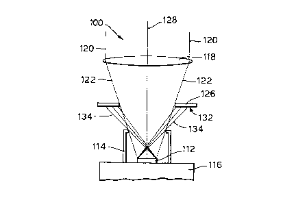
Un système optique à infrarouges (100) comprend une lentille (118) formant l'image d'une scène éloignée sur un détecteur (112) protégé par un écran froid (114). Les radiations parasites incidentes sur le détecteur (112) sont diminuées grâce à une barrière optique constituée par une diode émettrice de lumière (DEL) (126) produisant une luminescence négative. La DEL (126) émet moins de radiations que le fond et contribue moins au bruit de fond du détecteur de photons qu'une barrière optique ne présentant pas une luminescence négative.


Abrégé anglais


An infrared optical system (100) incorporates a lens (118) imaging a remote
scene onto a detector (112) within a cold shield (114). Stray radiation
incident on the detector (112) is reduced by an optical stop in the form of a
light emitting diode (LED) (126) producing negative luminescence. The LED
(126) emits less radiation than background, and contributes less to the
detector photon noise than an optical stop not exhibiting negative
luminescence.

Revendications

Note : Les revendications sont présentées dans la langue officielle dans laquelle elles ont été soumises.


8
CLAIMS
1. An infrared optical system including detecting means (112) and an optical
stop
(126) arranged to exclude stray radiation from reaching the detecting means
(112),
characterised in that the optical stop (126) is arranged to exhibit negative
luminescence to reduce radiation incident on the detecting means (112).
2. A system according to Claim 1 characterised in that the optical stop
incorporates a
hole which is disposed coaxially with an optical axis (128) of the system
(100).
3. A system according to Claim 1 or 2 having a single objective lens (118) for
directing infrared radiation to the detecting means and a cold shield (114)
for the
detecting means, characterised in that the optical stop (126) is located
between the
lens (118) and cold shield (114).
4. A system according to Claim 1 or 2 having a plurality of focusing elements
arranged in combination to image a scene onto the detecting means,
characterised
in that the optical stop (126) is positioned interjacent the focusing elements
and
detecting means of the system.
5. A system according to Claim 4 characterised in that the optical stop (126)
is
disposed between the detecting means (112) and that focusing element which is
nearest to the detecting means.
6. A system according to Claim 4 characterised in that the optical stop (126)
is
positioned at an intermediate focal plane within the plurality of focusing
elements.
7. A system according to Claim 4, 5 or 6 characterised in that it includes
means for
scanning a scene over the detecting means.

'
9
8. A system according to claim 1 or 2 arranged to
scan a scene over the detecting means, characterised in that
the optical stop (126) is disposed between detecting
means and an optical element nearest to the detecting means.
9. An imaging system according to any one of claims 1
to 8 characterised in that the optical stop (126) at least
partly comprises semiconducting material which is
electrically biasable to provide negative luminescence.
10. An imaging system according to claim 9
characterised in that the semiconducting material is cadmium
mercury telluride, an indium antimonide based material or
any other ternary Group II-VI compound exhibiting negative
luminescence.
11. A method of shielding an infrared detector (112)
from extraneous radiation (134), the method comprising the
steps of:-
(a) providing the detector with an optical stop
(126) incorporating an entrance pupil, the optical stop
(126) at least partly comprising negative luminescence
material;
(b) electrically controlling the negative
luminescence material to provide for its infrared emission
to be at a lower than ambient level: and
(c) focusing radiation from a scene via the
entrance pupil of the negative luminescence optical stop
(126) onto the detector (112).

Description

Note : Les descriptions sont présentées dans la langue officielle dans laquelle elles ont été soumises.


CA 022311~6 1998-03-0~
WO 97/18448 PCT/GB96/02777
INFRARED OPTICAL SYSTEM
This invention relates to an infrared optical system, and more particularly to noise
reduction in such a system incorporating a background limited detector.
An infrared detector is said to be "background limited" when the detector noise is
predomin~ntiy due to fluctuations in the rate at which photons reach it. Such a
detector in an infrared optical system will receive photons both from an imaged scene
and from sources of stray radiation which do not contain scene hlfc,.lll,iLion. If stray
0 radiation can be reduced or elimin~te-l detector noise is reduced without affecting
photons from the scene and the system signal to noise ratio is therefore improved.
To reduce stray radiation in infrared optical systems employing a cooled array of
detector elt?ment~, it is known to employ a shield which is itself cooled by the15 detector cooling a~ u~. The shield is cooled to reduce its thermal emission
re~ hin~ the detector array. However, in practice it is difficult to provide an efficient
cold shield. The problem occurs because of the finite size of the detector array. In
order to avoid vi~nt?ttin~ of the elements at the edge of the array, the size of the cold
shield aperture must be increased, making it less efficient. The problem is reduced
20 by using a larger cold shield more remote from the detector array, but this gives rise
to cooling difficulties. A large cold shield increases cooling a~aldLus requirements
and cool down time, and a small cold shield is inefficient in excluding stray
radiation. This problem is particularly severe in infrared optical systems having a
high f-number and/or in those incorporating a large detector such as a long linear
25 array or a two--lim~n~ional array of detector el~ment~
One approach to re~ cing stray light is to position an uncooled concave mirror
around a lens in the infrared optical system responsible for im~gin~ a scene onto the
detector. The mirror has a central hole to accommodate the lens. The mirror radius
30 of curvature is equal to the mirror-detector separation so that the detector coincides
with its image. The mirror necessarily has low emissivity and so generates relatively

CA 022311~6 1998-03-0
WO 97/18448 PCT/GB~)C~ 7
few photons. However, the mirror can reflect stray radiation to the detector, there
remains residual emission from the mirror which causes difficulty and the mirrorgives alignrnent problems.
5 It is an object of the invention to provide an alternative form of infrared optical
system.
The present invention provides an i-~L~ed optical system including ~letecting means
and an optical stop arranged to exclude stray radiation from rP~hing the detecting
I o means, characte}ised in that the optical stop is arranged to exhibit negative
luminescence to reduce radiation incident on the rietecting means.
The invention provides the advantage that the ~etecting means is shielded from stray
radiation by the optical stop without the penalty of receiving as much radiation as
ls that from a stop without negative IllminPscence characteristics but of equivalent
nature otherwise.
The optical stop preferably incol~o.dles a hole which is disposed coaxially with an
optical axis of the system.
The system may have a single objective lens for directing infrared radiation to the
~etectin~ means and a cold shield for the detecting means, the optical stop being
located between the lens and cold shield.
2s The system may alternatively have a plurality of focusing elements arranged in
combination to image a scene onto the lletecting means, the optical stop being
positioned interjacent the focusing elements and detecting means of the system. The
optical stop may be positioned between the detecting means and that focusing
element which is nearest to it or at an intermediate focal plane within the plurality of
30 focusing element~ The system may include means for sc~nning a scene over the
cletecfing means.

CA 0223ll56 l998-03-05
WO 97/18448 PCT/GB96/02777
The system may incorporate scSlnning means arranged to scan a scene over the
detecting means. the optical stop being disposed between the cletecting means and an
optical element which is nearest to the ~etecting means.
S
The optical stop may at least partly comprise semicondllcting m~t-~ri~l which iselectrically biasable to provide negative lllminescence. In a ~ ~fc~-~d embodiment
the semiconducting m~t-?ri~l is c~miunn mercury telluride or an indium antimonide
based material. This may alternatively be any other ternary Group I~-VI compoundlo (e.g. mercury zinc telluride, mercury m~ng7~n~se telluride, mercury m~ ;ul,
telluride, etc.) exhibiting negative lnminescence
In a further aspect the present invention provides a method of shielding an infrared
detector from exkaneous radiation, the method co~ ing the steps of:-
(a) providing the detector with an optical stop incol~-ol~illg an entrance pupil, the
optical stop at least partly comprising negative lnmintosc~nce material;
(b) electrically controlling the negative lnmin~ct~n~e material to provide for its
infrared emission to be at a lower than ambient level; and
(c) focusing radiation from a scene via the entrance pupil of the negative
ll~rninescPnce optical stop onto the detector.
25 This method provides the advantage of improved quality th~rm~l im~gin~ without
significant cost to other operative features of the imager.
In order that the invention might be more fully understood, an example thereof will
now be described, with reference to the accompanying drawings, in which:-
Figure I is a schematic drawing of a prior art infrared optical system: and

CA 022311~6 lsss-03-o~
wo 97/18448 PcT/Gs96lo2777
Figure 2 is a schem~tic drawing of an illrld~d optical system of the invention.
Referring to Figure 1, a prior art cold shielded infrared optical system of the im~ing
s kind is shown and is inc~ t~ generally by 10. The system 10 incol~o~dles an
inf~ared detector 12 located within a cold shield 14 and mounted on a cooled support
16. The detector 12 may be an array of detector elements or a single such element. It
lies in the focal plane of an objective lens 18, which produces an image of a remote
scene (not shown) upon it as in~iic~te(~ by rays of light 20 and 22.
0
The cold shield 14 is intenllecl to restrict radiation incident on the detector 12 to that
focused upon it by the lens 18 and ~ from the remote scene. However,
despite the cold shield 14, it is possible for stray light rays which are not received
directly from the remote scene to reach the detector 12. This is indicated by light
ls rays 24, which ori~in~te from directions outside the cone of rays bounded by rays 22
and incident on the detector 12 from the lens 18. ~n consequence. the detector noise
due to incident photons is higher than would be the case were incident light to be
limited to the cone of rays bounded by rays 22.
20 It would be possible to improve matters by increasing the size of the cold shield 14
reducing the separation between its upper surface and the lens 18. This is however
unattractive because it increases therrnal mass, cool down time and cooling capacity
J I ~ent~.
25 Referring now to Figure 2, there is shown a cold shielded infrared optical system of
the invention indicated generally by 100. Parts equivalent to those previously
described are like referenced with a prefix 100.
The system 100 incorporates an in~rared detector 112 within a cold shield 114, the
30 detector and shield both being mounted on and in thermal equilibrium with a cooled
support 116. An obiective lens 118 focuses parallel light rays 120 from a remote

CA 02231156 lsss-03-05
WO 97/18448 PCT/GB96/02777
scene onto the detector 112 as intlic~tecl by convergent rays 122. the detector lying in
the focal plane of the lens.
A light emitting diode (LED) 126 incorporating an entrance pupil is located at an
s interrnediate position between the cold shield I14 and the lens 118, and is coaxial
with the lens optical axis 128. The LED 126 is of the kind which provides negative
in~scen~e in response to bias signals of the a~ u~;at~ polarity. The shape of the
LED 126 and ~ ce pupil is dependent on the shape of the detector 112 used in thesystem 100. In the case of a two--limPn~ional ~ul~L~ ially square array of detector
lo element~ or for a single detector elem~nt the LED 126 should be annular. If
however, the detector array is subst~n~i~lly one-(1i,.~e~.~ional then the LED 126 and
entrance pupil function optimally if they are oval and elongated along the detector
axis.
5 The phenomenon of negative l--min~sc~ e as exhibited by the LED 126 is known.
It relates to emission of less radiation than a background level, and is described by
Bolgov et al, in Semiconductors 27(1), January 1993. It is also described by Berdahl
et al, Infrared Physics Vol 29, No 24, pp 667-672, 1989. Suitable m~tPri~ls for
negative Illmin~scen-e device m~nllf~-~tllre include cadmium mercury telluride,
20 indium antimonide and other m~teri~l~ from ternary Group II-VI semiconductor
systems.
The LED 126 has an active lower surface 132 which is responsible for negative
lumint?scence. The surface 132 therefore emits fewer photons than a surface in
2s thermal equilibrium with its surrolln(lin~s. Photons in~ic~tPtl by light rays such as
134 passing from the detector 112 are absorbed by the surface 132~ which returns a
lower intensity photon flux than a conventional optical shield at the same
t~ ldL~Ire as this surface. The surface 132 consequently acts as an optical stopwhich prevents stray light reaching the detector 112 whilst itself r~ ting to a lesser
30 e~ctent than a norrnal optical stop. Stray radiation equivalent to rays 24 in Figure 1 is
therefore largely excluded from reaching the detector 112. and the latter does not

CA 022311~6 1998-03-0~
WO 97/18448 PCT/GB96/02777
receive as much radiation as that which would reach it from an uncooled surface
which did not exhibit negative lllm;nescençe but which was otherwise of equivalent
structure and properties. Since the LED ~26is not required to cool down. it can be t,
switched on quickly avoiding the need for a long cool down time associated with a
5 large cold shield.
Moreover, if the LED 126 provides a sufficiently high m~gnitll~ç of negative
lnmin~cence, it will provide additional cooling ffir the detector 112. The criterion
for this is that the radiation emitted by the detector 112 which is incident on the LED
o 126is greater than the radiation emitted by the LED 126 which is absorbed by the
detector 112. The benefit is that the cooling capacity required for the support 116 is
reduced as COl~ d to what would otherwise be a~loyliate~
The optical system 100 is shown with a single objective lens 118 im~ing a remote15 scene onto the detector 112. It is known to have more complex im~gin~ systemsemploying multiple lenses and/or mirrors to image a scene. In these systems,
exclusion of stray radiation is best performed if the LED126is located between the
~I.otector and the final focusing element (lens or mirror) nearest to it. ~urther lenses
or mirrors between the LED and detector would give more scope for stray light to20 reach the detector. However design constraints may favour use of a smaller LED
126. The size of the LED device can be minimi~ec~ if it is placed at an intermediate
focal plane within the multiple arrangement of lenses and/or mirrors. Thus the loss
in exclusion ~ o-l-lance of the LED has to be b~l~nce(l with the advantages to be
had in the fabrication of a smaller device.
A further embodiment of the invention is provided by inco.yoldLion of the negative
ll-mine~cçnce LED 126 into a sç~nning thçrrn~l imager. Generally, such im~gers
additionally include a mechanical sc~nning mechanism arranged to scan a large scene
area over a detector. Again a balance has to be sought between maximising the
30 excluding capability of the LED 126 by locating it between the detector and the final

CA 02231156 1998-03-05
WO 97/18448 . PcTl(;l~5cl~27 / l
(closest) element of the combined focusing/scz~nning system and the advantages
gained in using a smaller device located about an interrnediate focal point.

Dessin représentatif
Une figure unique qui représente un dessin illustrant l'invention.
États administratifs

2024-08-01 : Dans le cadre de la transition vers les Brevets de nouvelle génération (BNG), la base de données sur les brevets canadiens (BDBC) contient désormais un Historique d'événement plus détaillé, qui reproduit le Journal des événements de notre nouvelle solution interne.

Veuillez noter que les événements débutant par « Inactive : » se réfèrent à des événements qui ne sont plus utilisés dans notre nouvelle solution interne.

Pour une meilleure compréhension de l'état de la demande ou brevet qui figure sur cette page, la rubrique Mise en garde , et les descriptions de Brevet , Historique d'événement , Taxes périodiques et Historique des paiements devraient être consultées.

Historique d'événement

Description Date
Inactive : CIB expirée 2022-01-01
Le délai pour l'annulation est expiré 2011-11-14
Lettre envoyée 2010-11-12
Inactive : CIB de MCD 2006-03-12
Inactive : Lettre officielle 2003-11-17
Lettre envoyée 2003-10-21
Inactive : Correspondance - Transfert 2003-10-21
Accordé par délivrance 2003-05-20
Inactive : Page couverture publiée 2003-05-19
Préoctroi 2003-03-05
Inactive : Taxe finale reçue 2003-03-05
Un avis d'acceptation est envoyé 2002-09-12
Lettre envoyée 2002-09-12
Inactive : Approuvée aux fins d'acceptation (AFA) 2002-09-03
Modification reçue - modification volontaire 2002-07-16
Inactive : Dem. de l'examinateur par.30(2) Règles 2002-05-29
Lettre envoyée 2001-08-24
Requête d'examen reçue 2001-07-25
Exigences pour une requête d'examen - jugée conforme 2001-07-25
Toutes les exigences pour l'examen - jugée conforme 2001-07-25
Inactive : CIB en 1re position 1998-06-05
Symbole de classement modifié 1998-06-05
Inactive : CIB attribuée 1998-06-05
Inactive : Notice - Entrée phase nat. - Pas de RE 1998-05-21
Demande reçue - PCT 1998-05-20
Demande publiée (accessible au public) 1997-05-22

Historique d'abandonnement

Il n'y a pas d'historique d'abandonnement

Taxes périodiques

Le dernier paiement a été reçu le 2002-10-17

Avis : Si le paiement en totalité n'a pas été reçu au plus tard à la date indiquée, une taxe supplémentaire peut être imposée, soit une des taxes suivantes :

  • taxe de rétablissement ;
  • taxe pour paiement en souffrance ; ou
  • taxe additionnelle pour le renversement d'une péremption réputée.

Les taxes sur les brevets sont ajustées au 1er janvier de chaque année. Les montants ci-dessus sont les montants actuels s'ils sont reçus au plus tard le 31 décembre de l'année en cours.
Veuillez vous référer à la page web des taxes sur les brevets de l'OPIC pour voir tous les montants actuels des taxes.

Titulaires au dossier

Les titulaires actuels et antérieures au dossier sont affichés en ordre alphabétique.

Titulaires actuels au dossier
QINETIQ LIMITED
Titulaires antérieures au dossier
CHARLES THOMAS ELLIOTT
NEIL THOMSON GORDON
RALPH STEPHEN HALL
TIMOTHY ASHLEY
Les propriétaires antérieurs qui ne figurent pas dans la liste des « Propriétaires au dossier » apparaîtront dans d'autres documents au dossier.
Documents

Pour visionner les fichiers sélectionnés, entrer le code reCAPTCHA :


Pour visualiser une image, cliquer sur un lien dans la colonne description du document. Pour télécharger l'image (les images), cliquer l'une ou plusieurs cases à cocher dans la première colonne et ensuite cliquer sur le bouton "Télécharger sélection en format PDF (archive Zip)" ou le bouton "Télécharger sélection (en un fichier PDF fusionné)".

Liste des documents de brevet publiés et non publiés sur la BDBC .

Si vous avez des difficultés à accéder au contenu, veuillez communiquer avec le Centre de services à la clientèle au 1-866-997-1936, ou envoyer un courriel au Centre de service à la clientèle de l'OPIC.


Description du
Document 
Date
(aaaa-mm-jj) 
Nombre de pages   Taille de l'image (Ko) 
Description 1998-03-04 7 284
Revendications 1998-03-04 2 69
Abrégé 1998-03-04 1 48
Dessins 1998-03-04 1 15
Revendications 2002-07-15 2 73
Dessin représentatif 1998-06-10 1 6
Avis d'entree dans la phase nationale 1998-05-20 1 193
Courtoisie - Certificat d'enregistrement (document(s) connexe(s)) 1998-05-20 1 117
Rappel de taxe de maintien due 1998-07-13 1 115
Rappel - requête d'examen 2001-07-11 1 118
Accusé de réception de la requête d'examen 2001-08-23 1 194
Avis du commissaire - Demande jugée acceptable 2002-09-11 1 163
Avis concernant la taxe de maintien 2010-12-23 1 171
Correspondance 2003-03-04 1 40
Correspondance 2003-11-16 1 8
PCT 1998-03-04 11 297