Note : Les descriptions sont présentées dans la langue officielle dans laquelle elles ont été soumises.
CA 02231243 1998-03-04
W O 97/13346 PCT~US96/15737
ATM SWITCH WITH VC PRIORITY BUFFERS
BACKGROUND OF THE INVENTION
1. Field of the Invention
~ The invention relates to an asynchronous transfer mode (ATM)
network switch. More particularly, the invention relates to an
ATM switch having cell buffers for each virtual connection (VC)
and means for outputting cells according to their VC priority.
2. State of the Art
In ATM data transmission, cells of data conventionally
comprising fifty-three bytes (forty-eight bytes carrying data and
the remaining five bytes defining the cell header, the address
and related information) pass through the network on a virtual
connection at an agreed upon rate related to the available
bandwidth and the level or service paid for. The agreed upon
rate will relate not only to the steady average flow of data, but
will also limit the peak flow rates.
Over an extensive network, cells on a virtual connection can
become bunched together with different cells having different
delays imposed upon them at different stages, so that the cell
flow on a VC then does not conform with the agreed upon rates.
To prevent rates being exceeded to the detriment of other VCs in
the network, the network will include, for example at the
boundary between different networks, means for policing the flow.
The flow policing means typically includes a "leaky bucket"
device which assesses the peak and average flow rates of cells on
a VC and if required either downgrades the cells' priority or
discards cells. An example of such a device is disclosed in co-
owned UK Patent Application No. 9505358.3 which is hereby
incorporated herein in its entirety.
Since policing can result in the discarding of cells which
should not be discarded, it is desirable to effect "traffic
shaping" to space out the cells on a VC sufficiently so as to
CA 02231243 1998-03-04
WO 97/13346 PCT~US96/15737
ensure that they meet the agreed upon rates, and in particular
the peak rates. A problem with traffic shaping is that it is
desirable to delay the transmission of cells by variable amounts
in an attempt to avoid cell loss. In practice, however, variable
cell delay has been difficult to implement. Co-owned UK Patent
Application No. 9509483.5, which is hereby incorporated herein in
its entirety, discloses an ATM switch with a traffic shaping
mechanism which delays the transmission of incoming cells by
varying amounts of time and which accounts for both peak and
average cell flow rates. The traffic shaping mechanism broadly
comprises means for det~rm;n;ng for each cell received an onward
transmission time dependent upon the time interval between the
arrival of the cell and the time of arrival of the preceding cell
on the same VC, buffer means for storing each new cell at an
address corresponding to the onward transmission time, and means
for outputting cells from the buffer means at a time
corresponding to the address thereof. The traffic shaping
mechanism results in cells being output at a rate which is
related to the rate at which they are received which eliminates
or m; n; m; zes bunching.
In some instances, however, it is desirable to provide a
more even output of cells, regardless of the rate at which they
are received. For example, different virtual connections may
have different priority levels. Presently, the ATM standard
provides for four different priority levels. In order to assure
that a priority level is maintained, it may be necessary that
cells having a high priority level be output before cells having
a low priority level, regardless of the rate at which the cells
are received.
SUMMARY OF THE INVENTION
It is therefore an object of the invention to provide an ATM
switch with means for controlling the flow of cells through the
switch according to VC priority.
CA 0223l243 l998-03-04
. W O 97/13346 PCTAJS96/15737
It is also an object of the invention to provide an ATM
switch with means for controlling the flow of cells through the
switch according to VC priority and with means for preventing
blockage of low priority cells.
It is another object of the invention to provide an ATM
switch with means for controlling the flow of cells through the
switch according to VC priority and which also allows traffic
shaping.
In accord with these objects which will be discussed in
detail below, an ATM switch according to the invention includes a
plurality of slot controllers each having at least one external
network link and a link to a switch fabric, the slot controllers
receiving ATM cells from the network and transmitting cells to
other slot controllers via the switch fabric and receiving cells
from the switch fabric and transmitting cells onto the network.
Each slot controller is provided with a plurality of FIFO
buffers, one cell FIFO for each VC established on the switch and
one arbitration FIFO for each priority level, and a FIFO
controller. According to the methods of the invention, when a
cell enters a slot controller, the cell header is eX~m; ned to
determine the VCI and the priority level. The slot controller
examines the switch fabric to find a path for the VC, selects a
VC FIFO for the VC, pushes the cell into the VC FIFO, increments
a counter for the VC FIFO, and, if the VC FIFO was previously
empty, writes a pointer to the arbitration FIFO for the priority
level of the cell FIFO. The arbitration FIFOs are ~X~m; ned
according to a schedule and cells are popped from VC FIFOs
according to priority for exit ~rom the slot controller.
According to one embodiment of the invention, the highest
priority arbitration FIFO is always examined ~irst and none of
the lower priority arbitration FIFOs are examined unless the
highest priority arbitration FIFO is empty. According to another
embodiment of the invention, timers are set for the lower
priority arbitration FIFOs and if a timer expires for a lower
priority arbitration FIFO, it is ex~m; ned regardless of the
CA 02231243 1998-03-04
W O 97/13346 PCTAJS96/15737
contents of the highest priority arbitration FIFO. According to
still another embodiment of the invention, the slot controllers
are coupled to two switch fabrics and two sets of arbitration
FIFOs are used, one set for each switch fabric. Prior to popping
a cell from a FIFO into the switch fabric, the switch fabric is
~x~m; ned to determine if the path is broken and whether an
alternate path exists through the second switch fabric. If an
alternate path is available, the cell is not sent, but the
pointer for the VC FIFO is pushed into the corresponding
arbitration FIFO for the second switch fabric.
According to the invention, the FIFO buffers may be arranged
only to buffer the flow of cells from the slot controller into
the switch matrix. Alternatively, a second set of FIFO buffers
may be arranged to buffer the flow of cells from the switch
matrix into the slot controller. The buffering system of the
invention may be used with or without traffic shaping
Additional objects and advantages of the invention will
become apparent to those skilled in the art upon reference to the
detailed description taken in conjunction with the provided
figures.
BRIEF DESCRIPTION OF THE DRAWINGS
Figure 1 is a high level schematic diagram of an ATM switch
according to the invention;
Figure 2 is a high level schematic diagram of a slot
controller according to a first embodiment of the invention;
Figure 3 is a high level schematic diagram of a cell
buffering system according to one embodiment of the invention;
Figure 4 is a schematic flow chart of how cells entering the
buffering system are handled;
CA 02231243 1998-03-04
W O 97/13346 PCTrUS96/15737
Figure 5 is a schematic flow chart of how cells exiting the
buffering system are handled; and
Figure 6 is a high level schematic diagram of a cell
buffering system according to another embodiment of the
invention.
DETAILED DESCRIPTION OF THE PREFERRED EMBODIMENTS
Referring now to Figure 1, an ATM switch 10 according to the
invention includes a plurality of controllers (which are often
called "slot controllers' or "link controllers") 12a-12g and two
dynamic crosspoint switch fabrics 14, 14'. Each slot controller
has at least one external link 16a-16h to an ATM network (not
shown), an input link 18a-18h to the switch fabric 14, an output
link 20a-20h from the switch fabric 14, an input link 18'a-18'h
to the switch fabric 14', and an output link 20'a-20'h from the
switch fabric 14'. This general arrangement is described in co-
owned UK Patent Application No. 9507454.8 and UK Patent
Application No. 9505358.3 which are hereby incorporated herein in
their entireties.
As shown generally in Figure 2, each slot controller 12 has
an input cell processor 22, an output cell processor 24, and a
cell buffering system 26. According to a first embodiment of the
invention, the cell buffering system 26 is coupled to the input
cell processor 22 for buffering cells received from the ATM
network before they pass through the switch 10. In this
embodiment of the invention, the output cell processor 24 is
conventional and handles such functions as writing cell headers
with new VPI/VCI information before passing cells onto the
network. The input cell processor 22 is unconventional in that
it controls the buffering system 26 in addition to other
conventional functions such as reading cell headers and routing
cells through the switch fabric to another slot controller.
CA 02231243 1998-03-04
W O 97/13346 PCT~US96/15737
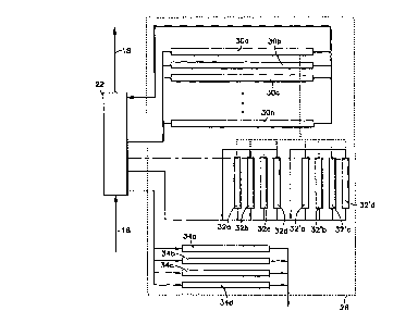
Turning now to Figure 3, the buffering system 26 generally
includes a plurality of VC FIFOs 30a, 30b, 30c, ..., 30n , a
plurality of priority level arbitration FIFOs 32a-32d, 32'a-32'd,
and a plurality of OAM FIFOs 34a-34d. The FIFOs are coupled to
the input cell processor and controlled by the input cell
processor as described below with reference to Figures 4 and 5.
According to the presently preferred embodiment of the invention,
the VC FIFOs are not individual hardware components but are
rather dynamically configured in RAM as needed. The number of
FIFOs created depends on the number of VCs being handled by the
particular slot controller. According to the invention, when a
cell is inspected by the cell processor 22 to determine the VCI
of the cell, a FIFO is created for that VC (if one does not
already exist). Typically, each VC FIFO would be a 64K FIFO,
although FIFOs of different sizes could be used depending on the
number of cells expected for a particular VC. The arbitration
FIFOs are preferably also dynamically configured in RAM. The
number of arbitration FIFOs corresponds to the number of priority
levels for VCs through the switch. As shown in Figure 3, there
are four arbitration FIFOs representing the current ATM priority
levels of "0" through "3" ("0" being the highest priority). In
the presently preferred embodiment, a separate set of arbitration
FIFOs is used for each switch fabric. Thus, as shown in Figure
3, FIFOs 32a-32d would be used for switch fabric 14 (Figure 1)
and FIFOs 32'a-32'd would be used for switch fabric 14'. The OAM
FIFOs 34a-34d are also preferably dynamically configured in RAM.
The number of OAM FIFOs corresponds to the number of priority
levels. The input cell processor 22 utilizes the OAM FIFOs to
buffer Operations and Maintenance cells which are handled by an
OAM processor (not shown).
The operation of the buffering system 26 is further
illustrated with reference to Figures 4 and 5 where Figure 4
illustrates cells entering the buffer system and Figure 5
illustrates cells exiting the buffer system.
CA 02231243 1998-03-04
WO 97/13346 PCT/US96/15737
Turning now to Figure 4, when a cell enters the input cell
processor, the header is exAm;ned at 50 and the VCI and priority
level are determined at 52. The cell processor inspects the
switch fabric at 54 to determine whether a path is available for
the VC. If, at 56, it is determined that no path exists for the
VC, the cell is discarded at 58. If a path does exist, the cell
processor pushes the cell into VC FIFO(n), where "n" represents
the VC, and increments a cell counter for VC FIFO(n) at 60 . If
it is determined at 62 that the cell count for VC FIFO(n) is "1",
i.e. that the FIFO was previously empty, a pointer pointing to VC
FIFO(n) is written and pushed at 64 into the appropriate
arbitration FIFO depending on the priority level of the cell
which was determined at 52. The cell processor then returns to
50 to examine the next cell received from the network. If it is
determined at 62 that the VC FIFO was not previously empty, no
pointer is written and the cell processor returns to 50 to
eX~m;ne the next cell received from the network. This process is
repeated for each cell received by the input cell processor and
new VC FIFOs are created as needed for new VCs. Similarly, empty
VC FIFOs are released from RAM so that RAM is made available for
new VC FIFOs. As the above described process continues, the cell
processor outputs cells to the switch fabric from the VC FIFOs
according to a selected procedure. Figure 5 shows a presently
preferred procedure with optional portions shown in phantom line
boxes.
Turning now to Figure 5, the output procedure starts at 70.
According to the essential principles of the invention, the
arbitration FIFOs are examined to determine whether they contain
pointers to VC FIFOs. In a simplified embodiment of the
invention, the highest priority FIFO(0) is always examined first
at 72. If the FIFO is not empty, the top pointer in the FIFO is
popped at 74. At 76, the VC FIFO to which the pointer points is
popped and the cell count for the VC FIFO is decremented. If it
is determined at 78 that the cell count of the VC FIFO is zero,
the procedure returns to the start 70 and ex~m; nes the
arbitration FIFO(0) again at 72 . If it is determined at 78 that
CA 02231243 1998-03-04
WO 97/13346 PCT~US96/15737
the cell count of the VC FIFO is not zero, the pointer to the VC
FIFO is pushed back into the arbitration FIFO(0) at 80 and the
procedure then returns to start 70 and ~X~m; nes the arbitration
FIFO(0) again at 72. According to this simplified embodiment of
the invention, none of the other arbitration FIFOs are ~X~m; ned
until the FIFO(O) is empty as determined at 72. If it is
determined at 72 that the arbitration FIFO(0) is empty, the
procedure goes to 82 and examines the contents of arbitration
FIFO(l). If the arbitratlon FIFO(1) is determined at 82 to
contain pointers, the top pointer is popped at 84, the
corresponding VC FIFO is popped at 86, the pointer is pushed back
into FIFO(1) at 90 if it is determined at 88 that the VC FIFO is
not empty, and the procedure returns to the start at 70. Only if
it is determined at 82 that the arbitration FIFO(1) is empty,
will the procedure go to 92 to examine the contents of
arbitration FIFO(2). If, at 82, it is determined that the
arbitration FIFO(1) is empty, the procedure described above is
repeated at 92-100 with respect to the arbitration FIFO(2). Only
if it is determined at 92 that the arbitration FIFO(2) is empty,
will the procedure go to 102 to examine the contents of
arbitration FIFO(3). If, at 92, it is determined that the
arbitration FIFO(2) is empty, the procedure described above is
repeated at 102-110 with respect to the arbitration FIFO(2).
The above simplified embodiment of the invention may be
enhanced by setting a timer for each of the three lower level
arbitration FIFOs. According to a second embodiment of the
invention, after the procedure starts at 70, timers are eX~m; ned
at 112-116 before examining the arbitration FIFO(0). In
particular, the timer for arbitration FIFO(1) is examined at 112
and if it has expired the procedure goes to 82 where the
arbitration FIFO(1) is ~X~m; ned as described above. In addition,
the timer for arbitration FIFO(1) is reset at 118 before the
procedure returns to start at 70. If the timer for arbitration
FIFO(1) has not expired as determined at 112, the timer ~or
arbitration FIFO(2) is examined at 114 and if it has expired the
procedure goes to 92 where the arbitration FIFO(2) is eX~m; ned as
CA 02231243 1998-03-04
W O 97/13346 PCT~US96/15737
described above. In addition, the timer for arbitration FIFO(2)
is reset at 120 before the procedure returns to start at 70. If
the timer for arbitration FIFO(2) has not expired as determined
at 114, the timer for arbitration FIFO(3) is ~x~m;ned at 116 and
if it has expired the procedure goes to 102 where the arbitration
FIFO(3) is ~x~m;ned as described above. In addition, the timer
for arbitration FIFO(3) is reset at 122 before the procedure
returns to start at 70. In this embodiment, the decisions at 82,
92, and 102 may be modified such that upon determining that an
arbitration FIFO is empty, the procedure returns to start, rather
than to examine the next arbitration FIFO.
In addition to the above, the procedure may be further
enhanced by testing whether paths through the switch fabric have
broken. For example, after the VC pointer is popped at 74, but
before the cell is popped from the VC FIFO into the switch, the
cell processor determines at 124 if the switch fabric path for
this VC is broken. If it is, the cell processor determines at
126 whether an alternate path is available through the second
switch fabric. If an alternative path is available, the cell
processor pushes the pointer at 128 into the appropriate
arbitration FIFO for the second switch fabric and then returns to
start at 70. If the path is broken and no alternative path is
available, the cell is discarded at 130. It will be appreciated
that this testing of the switch fabric may be implemented for
each arbitration FIFO. Therefore, the routines at 82-90, 92-100,
and 102-110 would be modified to include the same steps as
described with reference to 124-130. Those skilled in the art
will appreciate that the pointers stored in the arbitration FIFOs
preferably include information for output port number, switch
fabric preference, and priority, in addition to the VC
information.
v
According to still another embodiment of the invention, the
arbitration of the buffering system can be further enhanced to
deal with "blocked ports". According to this embodiment, another
arbitration FIFO is created for pointers to VCs having blocked
CA 02231243 1998-03-04
W O 97/13346 PCT~US96/15737
ports. The blocked port arbitration FIFO is then given the
highest priority. Since the presence of a single blocked port
could, under this system, prevent all cells from being
transmitted until a particular port becomes un-blocked, the
pointers in the blocked port arbitration FIFO are preferably
recycled each time a pointer encounters a blocked port. In other
words, when a pointer is popped from a blocked port arbitration
FIFO, the pointer is pushed back to the bottom of the FIFO if it
points to a VC which continues to have a blocked port. According
to a presently preferred implementation, a separate blocked port
FIFO is provided for each priority arbitration FIFO so that the
blocked ports are also dealt with according to priority level.
The cell buffering systems described above are suitably used
to buffer cells entering the ATM switch. However, similar
systems can be used to buffer cells exiting the ATM switch when
no traffic shaping is required, e.g. constant bit rate (CBR)
traffic. Alternatively, the buffering system described above can
be used in conjunction with the traffic shaping system described
in the above-referenced co-owned application. Still
alternatively, the buffering system described above can be
employed where the cells exit the switch and modified to
accomplish traffic shaping. Figure 6 shows a buffer system
according to the invention arranged to buffer cells exiting the
switch and for traffic shaping.
Turning now to Figure 6, the buffering system 226 is similar
to the buffering system 26 described above with similar
components identified with similar reference numerals increased
by 200. The system 226 generally includes a plurality of VC
FIFOs 230a, 230b, 230c, ..., 230n , a plurality of priority level
arbitration FIFOs 232a-232d, and a plurality of OAM FIFOs 234a-
234d. The FIFOs are coupled to the output cell processor 24 and
controlled by the output cell processor as described above with
the following differences. A separate set of priority
arbitration buffers is provided for each external data link on
the slot controller. For example, as shown in Figure 6, there
CA 02231243 1998-03-04
W O 97/13346 PCT~US96/15737
11
are eight arbitration FIFOs shown for each class of traffic 232a-
232d. This corresponds to eight external data links. The
arbitration FIFOs are preferably ex~m;ned for a particular
priority for each data link in sequence. In other words, the
first of eight FIFOs 232a is read for a pointer, then the next of
the eight FIFOs 232a is read for a pointer, until each of the
eight FIFOs 232a is read for a pointer. Otherwise, the
arbitration operates in substantially the same manner as
described above with regard to the system 26.
As shown in Figure 6, the buffering system 226 may also
include a set of traffic shaping buffers 235a-235d containing
pointers having addresses which correspond to the time at which
the cell pointed to is to be sent. This corresponds to the
traffic shaping system described in the previously referenced co-
owned patent application with the following difference: the
pointers in the traffic shaping buffers point to a VC FIFO rather
than to a particular cell. Depending on the type of VC, a
pointer to a VC FIFO ~230a, 230b, 230c, ..., 230n) may be written
in either a priority arbitration FIFO 232a-232d, or to an
appropriate traffic shaping FIFO 235a-235d.
There have been described and illustrated herein several
em~bodiments of a ATM switch with VC priority buffers. While
particular embodiments of the invention have been described, it
is not intended that the invention be limited thereto, as it is
intended that the invention be as broad in scope as the art will
allow and that the specification be read likewise. Thus, while
particular numbers and types of FIFO buffers have been disclosed,
it will be appreciated that other numbers and types of FIFOs
could be utilized. Also, while particular procedures have been
shown for reading the arbitration buffers, it will be recognized
that other types of procedures could be used. Moreover, while
particular configurations have been disclosed in reference to the
operations of the input and output cell processors, it will be
appreciated that other configurations could be used as well. For
CA 02231243 1998-03-04
W O 97/13346 PCT~US96/15737
12
example, the management of the arbitration and VC FIFOs could be
accomplished by a separate processor and not delegated to the
input and output cell processors. Furthermore, while the ATM
switch has been disclosed as having eight slot controllers and
the slot controllers have been shown with eight data links, it
will be understood that different numbers of slot controllers and
data links can be used.
It will therefore be appreciated by those skilled in the art
that yet other modifications could be made to the provided
invention without deviating from its spirit and scope as so
claimed.