Note : Les descriptions sont présentées dans la langue officielle dans laquelle elles ont été soumises.
CA 02231793 1998-03-06
W O 97/13358 PCT/~B96/n2347
-1 -
Thermal Imaqing Sysfem
This invention relates to a thermal imaging system of the kind in which a scene is
imaged by scanning.
Thermal imaging systems are known in the prior art. In principle, infrared radiation
emitted by a warm object is directed onto a photoconductive detector (see, for
example, Thermal Imaging Systems by J.M.Lloyd, Plenum Press, 1975) and the
thermal image is reconstructed from the electrical response. Coverage of a large10 scene area is generally achieved in one of two ways: imagers either sample
simultaneously different sections of a scene or image each component of a scene
sequentially. In the former case an array of detectors are used in a "staring" mode
and in the latter a mechanical scanning mechanism directs radiation from each pixel
of a scene onto a small detector area. A staring array i",ayi"~ system has the
15 advantage that it lends itself to compactness of design but suffers from many other
problems. Detecting elements rarely have uniform detectivities and responsivities, 11f
noise is relatively important and effective cold shielding poses further problems.
Scanning tlhermal imagers, although more cumbersome, offer conside, ~ble
advantage in requiring simpler and cheaper detector arrays. A third option is to use a
20 combination of both methods, namely, mechanical scanni"g of a large scene area
onto a small array of detectors. Individual scene pixels may be scanned sequentially
over a number of detectors, the signals from which are time delayed and integrated in
the thermal image resulting in either an improved sensitivity of image or ~ccept~'e
sensitivity being achieved with faster scan speeds. Furthermore, several pixels may
25 be scanned simultaneously by the use of multiple det~ctors.
There are considerable differences to be borne in mind when imaging thermal
wavelengths as opposed to optical photons. First, optical images are produced
~ primarily by reflection and reflectivity differences, and in this spectral region terrestrial
30 materials tend to have good reflectivities. Thermal images arise from self-emission
and emissivity differences and against a terrestrial background radiation cor,l,~s are
small and so object resolution is coarse. More effort has to be directed towardsimproving the contrast within a thermal image. Secondly, although it is
W O 97/133S8 CA 02231793 1998-03-06
PCT/GB96/02347
--2--
electromagnetic radiation which is detected, a thermal image is generally described in
terms of temperature. All contributions to the measured irradiance at any point in a
scene can conveniently be represented by an effective temperature at that point.This temperature is that at which an ideai black body would emit radiation with the
5 measured intensity.
A major advantage of scanni"g thermal imagers is that the detector signal can be ac
coupled to the signal processing system. Commonly a scene is ~isseçtecl by raster
scanning into a series of parallel lines covering its area. Insertion of a high pass
10 circuit between detector and amplifier eliminates th'e dc component of a signal and
transmits only variations as the scan progresses along a line. This has the
advantages of enhancing the contrast, eliminating any variability in the dc offset
voltage of different detectors and reducing the effects of detector 1/f noise. Image
defects arise however: a step function signal from the detector will be distorted as
15 c~p~cit~nce within the high pass circuit discharges and the output signal will suffer
from droop which in turn causes undershoot as the input step function returns tozero. In addition, the response of a high pass circuit is somewhat dependent on its
past history; in a multielement detector it is highly unlikely that all such circuits will
have received the same average signal and so channel responses will not be
20 uniform. Furthermore elimination of the dc component also removes the ~hsol~lte
temperature of the scene.
It is advantageous to restore some ~hsolut~ temperature reference to the image.
This can be important if, for exal, r'E, the horizon is to be seen and for radiometric
25 mo"ilori"5l of, for example, manufacturing processes To achieve this and also to
counter the image defects of droop, undershoot and channel nonuniformity a prior art
technique gives a reference signal to the dete.;lor at intervals during the scan. The
reference source is typically a convenient passive scene such as the interior of the
imager housing although an active source such as a heated strip can also be used.
30 The image is then displayed with the high frequency pixel to pixel variations within the
scene superimposed on the dc level provided by the reference temperature.
This method of artificial dc restoration is not ideal if the reference temperature is not
close to the scene average. An intermediate frequency variation in temperature will
, CA 02231793 1998-03 06
:
occur as the detector switches between scene and reference source and this will not
be immune to the effects of droop and undershoot. Furthermore detector
responsivity can vary widely with illumination intensity and so unifying the response of
a multidetector system at the reference temperature will not guarantee a consistent
5 response at the scene temperature. Unfortunately this problem is not easily
overcome. The situations in which thermal imaging systems are employed are many
and varied. Portability is frequently essential and it is not practical to provide as
many different temperature reference sources as there are scenes likely to be
imaged. An active source requires heating apparatus or more bulky cooling
10 apparatus ancl the time taken to reach desired te,,,perc-lures is often prohibitive.
An example of a prior art m~ltidetector scanning thermal imager which primarily
addresses the problem of non-u"iro",.ity of detector response is disclosed in USPatent Application No. 4 948 964. A ci~oppi"g mirror is arranged such that during
15 the reset portion of the scan two reference illuminations of differing i"lensilies are
incident on the detector array. For this i,ilensily (temperature) change the gain of
each detector is adjusted to ensure that uniform voltage responses are developed.
The thermal reference source used is a thermoelectric cooler which if possible, is
adjusted to the approximate average ler"~ erdlure of the scene in order that the gain
20 normalisation is perFormed within the dynamic range of the imager. This average
level provided by the cooler is also used as the cla",pi"g level in dc ,e:,loralion.
Alternative prior art radiation sources although not disclosed in the context ofimaging pr~cesses are ~~isclosecl in US Patent Ar.plic~l;on 4 561 786 and by Bolgov
25 et al. in UIR Sources with Barrier-Free Injection Mecl1an;~l"n Avtometriya No. 4 pp
8~ - 88 (1989). The former document ~iiscloses use of a light er"illi"5~ diode (LED) to
provide a reFerence signal which is of equivalent bl iyl ,l, .ess to target (scene)
emission at a particular wavelength in constructing a radiometer which is relatively
insensitive to surFace characteristics of the target being measured. Bolgov ~iiscloses
30 a crystal plate of i"l, i"sic InSb coated and etched such that one face of the plate has
a high carrier recombination rate (Sma,~) and the opposile face has a low
recombination rate (Smjn). The Hall effect is then used to concentrate carriers at one
or other of the faces. When carriers are concel,l,dlecl at the Smjn face the lower
AMENDE~ S~E~
~PEAJEP
CA 02231793 1998-03-06
-3a~
recombination rate results in an above-equilibrium distribution of carriers at this
surface and luminescent emission is observed. Converseiy concentration of carriers
at the smax face results in the crystal becoming depleted of charge carriers and below-
equilibrium radiation emission is observed from the Sm~n face.
It is an object of the invention to provide an alternative form of thermal imaging
system.
The present invention provides a thermal imaging system inco"~oraLi"g a scanning10 mechanism for scanning an observed scene onto a detecting element and a radiation
source arranged to provide illumination of the detecting element at a reference level
characterised in that the radia~ion source is a variable luminescence device (2~) of
semiconducting material and the system also includes means for adjusting the output
radiation intensity from the variable luminescence device to correspond more closely
15 to the mean lcl.lidliol1 intensity of the scene under observation and thereby to reduce
single-element imaging defects.
The invention provides the advantage that it is capable of providing a referencetemperature which is actively ~ljusted to co"es~,ond to the le",perdl,lre of a scene
20 under observation and so leads to l~sl~l~lion of ~hsolllte temperature to a thermal
image and recluced image defects.
The variable luminescence device is preferably co"l, ~ le to readjust the intensity of
flux e--,issior, to within 10% of a steady state value in seKling times of less than ten
25 seconds. The variable IL""i"escence device may be electrically co"l,-,llable and
~r- le of re~ijusting the inlel1sity of flux emission to within 1% of a steady state
value in settling times of less than one second. Operation within these limits may be
provided for if the variable lu",i-,escence device is a semiconducting device which in
a pref~r,t:d embodiment is an illrl;dred light emitting diode (IRLED) which is
AMI~NDE~
IPFA/EP
CA 02231793 1998-03 06
electrically biasable to provide both positive and negative infrared luminescence
emission relative to background radiation level and thereby to provide an effective
reference temperature which is not restricted to the system environment. This
provides capability for rapid adjustments to be made to the reference temperature
5 supplied by the IRLED. Active convergence of the reference temperature towardsthe scene temperature can be accomplished in as many steps as are necessary withvery little limitation imposed by the time taken to adjust the reference source to a new
temperature. Prior art imagers using heated strips or thermoelectric coolers as
references have unacceptably long waiting times as the reference temperature is
1 0 adjusted.
Suitable IRLEDs may be fabricated from cadmium mercury telluride or an indium
antimonide based material.
15 The switching means is preferably arranged to switch the detecting element tomonitoring the variable luminescence device between intervals of monitoring the
scene. In one embodiment the switching means is switchable between a first
configuration in which radiation from a scene under observation is incident on the
detecting element and a second configuration in which rddidliol1 from a variable20 luminescence device is incident on the detecting element. This provides the
advantage that the time for which the detector is idle i.e. monilo, ing neither scene nor
reference is reduced to the time taken to switch between these two configurations
only. Separate temperature references incorporated into prior art imagers require
switching between a number of configurations as a reference temperature nearest
25 the scene temperature is found and so s ~:itching time is increased accordingly.
The switching means pr~ferdbly possesses scanni~,g c~p~hi'ity. This provides theadvantage that "le-;hanical scanning of the scene and disco,lli"uous adoption ofscene and IRLED observation configurations are f~r~ t~t~d by just one component
30 mirror. Thus the entire imaging system is more portable. Scanlling may be twodimensional using either a single mirror or, more commonly, a compound mirror
system in which a rotating "drum" controls line scanning and a plane mirror controls
the frame scan.
AMENDED Sl IE~,
IPEA/EP
-
! CA 02231793 1998-03 06
The thermal irnaging system of the invention may include control means arranged to
supply a bias current to the variable luminescence device. The control means is also
arranged to generate a signal corresponding to the difference between mean scene5 temperature and effective luminescence device temperature when the system is
switched from scene to luminescence device observation. In response to this signal
it adJusts the Ibias current and hence the effective temperature of the luminescence
device in accordance with the magnitude of the signal and in a direction to reduce
said temperature difference. In this way active adjustment of the output of the
10 luminescence device so that it corresponds to the mean scene temperature is carried
out automatically by feedback. This requires no manual input or estimate of the
scene temperature.
More specifically the detecting element may be arranged to supply an output signal
15 to a capacitor which in tum is arranged to store the dc component thereof. The
control means ~,ererably includes a control circuit arranged to supply a bias current
to the variable luminescence device an integrator arranged to integrate input current
and second switching means a"arlged to direct towards the integrator charge flowing
from the capacitor as the stored dc component changes. In this embodiment when
20 the imaging system ~ I ,anyes from scene observation to lu m inescence deviceobservation the switching means provides a signal to the control circuit cor,~spondi-,g
to the difference between the mean scene te"~peral.lre and the effective IRLED
temperature. Furthermore the control circuit may be ar,~"ged to adjust the current
through the infrared lu"li"escence device after each change from scene to
25 luminescence device observation. This provides a means for ,~alisi"g the feedback
necess~ry to adjust the luminesce"ce device emission which can be implemented for
little cost.
In a further embodiment the imaging system prererably includes display means
30 a" dnged to display the ac temperature variations of the observed scene
superimposed on the temperature level provided by the i,.r,~r~d emission from the
variable luminescence device in order to provide an image with ~hsolute temperature
restored. Thi-; ensures ease of inte"u,~lalion of the thermal image.
AA/iENDED SHE~I,
IPEA/EP
CA 02231793 1998-03 06
In a further aspect the present invention provides a method of generating a reference
temperature for a scanning thermal imaging system, the method comprising the steps
of:-
(a) iliuminating a detecting element with a reference intensity of infrared radiation
from an electrically-controllable variable luminescence device of
semiconducting material;
(b) switching between a state of scene observation and a state of reference
signal observation and thereby generating a difference signal corresponding
to the difference between the mean intensity of infrared radiation emitted by
the scene under observation and that emitted by the variable luminescence
device;
(c) adjusting the current through the variable luminescence device to reduce thedifference signal generated in Step (b) and thereby causing the reference
intensity to correspond more closely to that of the mean level of infrared
emission from the scene under observation; and
(d) reconstructing a thermal image of the observed scene by superimposing the
scene variations in temperature on the ~hsol,~te reference level provided by
the variable luminescence device
whereby the generated reference temperdLure actively converges towards the
average temperature of the scene being observed and absolute temperature is
restored to a thermal image of the scene. Furthermore Steps (b) and (c) may be
repeated pe,iodically in order that the i"tensily of i"r,~,t d el~ission from the variable
luminescence device approaches the mean e",ission illL~nsiLy from the observed
scene via a feedback mechar,i;,,
This method of the invention provides the advantage that it restores the absolute
temperature to a thermal image of a scene and counteracts some of the image
defects caused by droop, undershoot and channel nonuniformity. In addition it lends
itself to implernentation in fast, portable imagers.
AM~NDED Sl IE~
IPEA/r p
CA 0223l793 l998-03-06
W O 97/13358 PCT/GB96/02347
--7--
In order that the invention might be more fully understood embodiments thereof will
now be described with reference to the accompanying drawings in which:
5 Figure 1 illLlstrates schematically a plan view of a proposed mode of operation for
restoration of the absolute temperature to a thermally imaged scene using a negative
/ positive lurninescence device;
Figure 2 illustrates schematically a sequence whereby an area is imaged by a
10 scanning thermal imager; ~ .
Figure 3 illustrates schematically an effective composite scene when a referencelevel is given to an imager after each scan line;
15 Figure 4 is a representation of an i,,rur,,,alion processing system of a thermal imager
which reconstructs the thermal image in response to output signals from a
photoconductive detector;
Figure 5 provides two graphs illustrating a step pulse voltage input and corresponding
20 output from a standard series resistor-capacitor circuit;
Figure 6 represents graphically the output voltage across the resistor of an RC circuit
which ac couples a detector when a thermal imager co"l~i";. ,9 the detector is
alternately receiving a reference signal and scanning a scene and for which the mean
25 scene temperature is higher than that of the reference;
Figure 7 illustrates the same output as Figure 6 except in this case the temperature
of the reference is adapted to match the mean scene temperature; and
30 Figure 8 is a representation of an i"ror"~lion processing system of another
embodiment of this invention in which the absolute te",per~lure is restored to athermal image generated when an array of detectors are scanned across a scene.
WO 97/13358 CA 0 2 2 317 9 3 l 9 9 8 - 0 3 - 0 6 PCT/GB96/02347
--8~
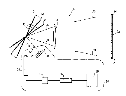
With reference to Figure 1, there is shown a plan view of a thermal imaging system
indicated generally by 10. The system 10 incorporates an objective lens ~1 whichfocuses infrared (IR) radiation, indicated for example by rays 12 and 14 and thick
arrows 16 and 18, onto an infrared photoconductive detector D1. A mirror system M1
5 either scans through a range of observation positions, defined in the plane of the
figure by the extremities 01 and 02 (indicated by grey coloration) or shifts
discontinuously to a cai;bralion position C (black) The scanning achieved by themirror M1 is two-dimensional although, for clarity, neither this nor a compound mirror
system are shown in the diay,~",. A linear representation of a scene being imaged is
depicted at 22 and two extreme regions are highlighted at 24, 26~ An infrared light
emitting diode (IRLED) 28 is mounted on a Peltier cooler / heater device 30~ When
the mirror M1 is in its calibration position C then IR radiation emitted by the IRLED 28
is reflected from this mirror and reaches the detector D1 as shown by ray path 32, 34.
The detector D1 is connected to an electronic processing circuit 35. A computer 36
processes information received from this circuit and passes information to a display
apparatus 38. These are conve"lional infrared imaging items and will not be
described further. The components of the system within the boxed area 80 are
described in more detail in Figure 4.
Figure 2 illustrates the dissection of the two dimensional scene 22 into a series of
scan lines. It is a view taken along the central axis of the optical system of Figure 1
and represents the projection of the detector D1 onto the scene 22 through the mirror
M1. The extreme regions 24 and 26 of Figure 1 are in fact lines corresponding to the
horizontal extremes of the scene 22. At any particular instant in time the thermal
imager 10 of Figure 1 images a single pixel area 40. Scan lines are illustrated by
horizontal lines 42, 44 and 46, 48. A second single-pixel area 50 illustrates the
overlapping of pixels in successive scan lines in order that an entire area S1 is
imaged.
Figure 3 is a representation of the activity of the imager 10. A pixel 60 identifies the
fraction of a scene which is imaged at any particular point in time. An arrow 66 t
indicates the scanning direction of the imager 10. Two scenes are shown in this
hgure a thermal reference source 62 at temperature T~ and a scene under
CA 0223l793 l998-03-06
W O 97/13358 PCTJGB96JD2347
--9--
observation 64 at mean temperature Ts. The areas shown are illustrative of the
proportion of time spent observing each source.
Figure 4 illustrates in more detail the detector D 1 together with the electronic
5 processing system 80. The output from the detector D1 is input to an RC circuit
comprising a coupling capacitor C, and resistor R,. The output from this circuit is
passed to an amplifier 82 and then to the computer system 36 which reconstructs the
image in a suitable form for the display apparatus 38. A second ,~si-tor R2 has a
much smaller resistance than R~ and so when a switch 84 is closed the ~pacitor C,
discharges through R2. A monitor 86 in conjunctior~ with R2 pe,ru,."s the function of
integrating the current flowing through R2 as the c~pacitor discharyes. A control
circuit 88 adjusts the current flowing through the IRLED 28 in ,~sponse to the
strength of signal it receives from the monitor 86. In operdlion the de~.o.;Lor D1
output signal gives rise to a voltage at a point 90 between C1 and Rl or R2 which will
be discussed later.
Figure 5 provides two graphs 102 and 103 illusll~Lillg a particular input voltage and
cor,esponding output voltage across the resistor of an RC circuit. A step function
input of strength Vjn and duration ~ is depicted by the line 104. The output voltage
with maximum value V0u~ is represented by the line 106. The phenomena of droop
and undershoot are illustrated by the sections of the line 106 denoted by 108 and 110
respectively.
Figure 6 represents y~phically the behaviour of the voltage at the point 90 of Figure
4 when the switch 84 is permanently open and the imager 10 alternately views thereference temperature Tl for time t~gf and scans the scene at mean ter"per~Lure Ts
for a time tScan. The form of the output voltage at 90 (y-axis) is plotted against time
(x-axis). Assuming Ts ~ Tl the voltage curve is i"~l;c.-l~cl yt:nerdlly by 120. Each
output step 122 124 is the result of temperature differences within the scene
superimposed on a decaying step output (108 in Figure 5).
Figure 7 represents y, ~phically the behaviour of the voltage at 90 when the switch 84
is operated as described below and the imager 10 alternately views the referencesource at temperature T1 for time t,~ and scans the scene at mean temperature Ts for
CA 02231793 1998-03-06
W O 97/13358 PCT/~Lr./~2347
,. .
-10-
a time tScan. The switch 84 is open for the time tScan during which the imager scans
the scene and closed for the time t,~f as the reference temperature is observed.Successive scan lines 140,144,148 lead to smaller voltage discontinuities 142, 146
as the IR emission of the IRLED 28 is increased until it corresponds to that emitted
5 from a scene at mean temperature Ts
The mode of operation of the invention will now be described in more detail.
Referring once more to Figure 1, infrared radiation en,andli,,y from a position 24
10 within the scene 22 is selected by the mirror M1 in position 01 and focused via a path
indicated by the arrow 16 and rays 12, 34. Similarly infrared radiation oriy;~lalillg
from the opposite extreme 26 of the scene 22 is focused onto the detector D1 when
the mirror M1 is in position 02 via a path indicated by the arrow 18 and ray 14,34. In
operation, the mirror M1 traverses the range 01 to 02 and this enables ,adidlion15 originating from all positions between 24 and 26 within the scene to be focused by
the lens L1 onto the infrared detector D1. Equivalently, taking the scene as
reference, the imager 10 scans across the scene 22 between posiLions 24 and 26.
This scanning process is illustrated more completely in Figure 2. Coverage of a two-
20 dimensional scene is ac,hi~ved by ~issectirlg the area into a series of scan lines.Imaging is not continuous in the vertical direction but the finite size of an imaged area
at each point of the scan means that overlap may be arranged between vertically
~~ispl~ced pixels such as 40 and 50. To achieve this area breakdown the mirror
system M1 (not shown) is a"~nyed to produce a horizontal scan from posilion 42 to
25 position 44 followed by a fast reset to position 46. This motion is ~pe~l~d and a
second scan line extends from 46 to position 48. A fast reset then directs IR
radiation from a position further down the scene edge 24 onto the detector D1 and
the entire scanning process is repeated until the area 51 has been imaged onto the
detector D1.
In a situation of radiative equilibrium the IRLED 28 emits as much radiation into its
surroundings as it absorbs from them. However this equilibrium situation is disturbed
by the application of an electric current. In such a situation the IRLED 28 will either
be a net emitter (positively luminescent) or a net absorber (negatively luminescent) of
-
CA 02231793 1998-03-06
IR radiation. Negative luminescence is a known phenomenon and will not be
described furlher see P.Berdahl et a/. in Infrared Phys. ~(24) 667 (1989) and
Bolgov et al., referenced herein. For IRLEDs, the mode of o~,erdlion depends on
whether the device is forward or reverse biased. The inlensily of IR radiation emitted
5 is dependent upon the bias current magnitude. For any particular value and direction
of bias current the IRLED 28 emits IR radiation with an intensity equal to that which
would be emitted by a black body at a particular tel"per~lure T~f. If the IRLED 28is
forward biased then T,ef will be hotter than the ambient temperature and if the IRLED
28 is reverse biased then T,ef will be colder than ambient. If the current through the
IRLED 28is increased then the flux emitted will be equivalent to that e",illed by a still
hotter body in the case of forward biasing and by an even colder body in the case of
reverse biasing. The IRLED 28is caliLr~l~d so that for any particular value of current
flowing and any sense of biasing the i"lensily of IR radiation emitted or absorbed by
the IRLED and hence its black body temperature equivalent are known. The Peltier15 device 30 sen/es to hold the te",per~lure of the IRLED 28 stable at the temperature
at which its IR e~ 5~iGn was calibl~led. Alternatively the IRLED 28is calibrated ove
the range of temperatures at which the imager is expected to operate which although
increasing the co" '~ y of the caliLr~lio" process removes the need for the Peltier
device 30.
As is con,r"or, in scar",ing ll,el",al i"~agera the detector is ac coupled; that is post-
detector ele- I,ul,ics respond to and ampli~ only the chal,ges in observed
tel "per~lure as the scan proy, ~sses. This conll dal-only image improves the
resol~tion dllai.,able but loses the r~solute scene temperature. To restore some25 ~hsolute temperature ,~:rt:rel~ce to the image a reference signal is given to the
detector at intervals during the scan. Figure 1 illustrates how the i,,,ay;~ly system 10
observes a reference signal provided by the IRLED 28 when the mirror M1 is at
position C. Fi~qure 3 illustrates the sequence ~l ,ereby the imager, via its field-of-view
pixel 60, allellldtely observes a II,el",al reference source 62 and conducts an active
30 scan of a scene of il,l~real 64. The thermal reference source is the IRLED 28emitting IR radiation with an i"l~l~sily coi,si~Lent with a temperature T1 and the scene
of interest has mean temperature Ts although it is the temperature varidlions about
this point which are measured by the imager 10.
AMENDED Si 1
IPtA!~ P
CA 02231793 1998-03-06
W O 97/13358 P~T/~B9~023~7
-12-
Figure 4 illustrates the processing of signals output from the detector element D1.
The ac coupling is provided by the capacitor C~ and resistor R~ which form a high
pass filter which attenuates the low frequency component of the output voltage from
the detector D1. The high frequency component of this signal (cor,espon~li"g to5 pixel-to-pixel temperature differences in the scene) is passed to the amplirier 82 and
then to the computer system 36 which reconstructs the image in a slr~~ e form for
the display 38 The switch 84 is open when the imager 10 is sca-",i.,g the II,er",al
scene and closed when the reference signal from the IRLED 28is observed. The
resistor R2 has a much smaller resistance than R, and when the switch 84 is closed
10 the current flowing through R2 is integrated and held by the integrator 86. The
current flow as the system switches from active scanning of the scene to observation
of the reference signal occurs when the capacitor C1 discharges (or cl~aryes) from a
level consi~ilent with the mean scene temperature to a level cons;~l~nL with theeffective ternperature of the IRLED 28. If the IR flux produced by the IRLED 2815 corresponds to that emitted by a black body of temperature T7 and the mean
temperature of the scene is Ts then the integrated current is a measure of the
difference between the mean thermal flux from the scene and that from the reference
diode which in turn is a measure of Ts~ T1. The control circuit 88 adjusts the current
flowing through the IRLED 28 in order to ",i";."ise this difference. The integrator 86
20 passes a signal to the circuit 88 the magnitude of which is ,, rupoi lio,~al to the extent
to which the two temperatures differ and whose sign i"dicales whether the l~r~rence
at T~ is hotter or colder than the scene at Ts. The control circuit 88 then adjusts first
the current through the IRLED 28 and if necess~ry the biasing direction in order that
the reference temperature can be made equal to the mean scene ter"perdlure Thus
25 both the positive and negative luminescence c~ ;ties of the IRLED 28 are
e~rlcited and the source and mean scene temperatures can be equa' se~ regar~lcssof whether the scene is hotter or colder than the ambient ler"per~l.lre of the imager.
Figure 5 provides graphs which illustrate the response 103 of an RC circuit to a step
30 function input voltage 102. Ideally the input voltage steps from 0 to a value Vjnl
remains constant for a time I and then drops suddenly to 0 as shown by the line 104.
The output voltage as measured across the resistor R, in Figure 4, rises quickly to its
maximum value V0ut in response to the input step to Vjn1 falls gradually as the
capacitor C~ ~in Figure 4) discharges with time constant R,C1 over the time ~ that the
CA 02231793 1998-03-06
W O 97tl3358 PCT/GB96/02347
-13-
input voltage remains constant and then drops by an amount VOut to a value below 0.
The behaviour of the output voltage is indicated by the line 106. The portion of the
line 106 as the voltage falls with time constant R~C~ 108 is known as droop and the
period for which the output voltage is below zero 110 is known as undershoot. Both
5 droop and undershoot degrade the thermal image. Droop can be reduced by
increasing l:he time constant R,C1 but this increases the duration of undershoot. In
this embodiment the time constant R~C1 is long compared with the time taken to scan
a line of the scene (line time) in order to minimise droop.
Consider the point 90 shown in Figvre 4 between C~ and R, or R2. If the switch 84 is
kept open and the imager observes the reference Lempeldlure T~ for time t,,?f and
scans the scene at mean temperature Ts for a time tScan then the voltage at point 90
varies as shown in Figure 6. This figure is a yl~phi~~l rep,t:se"L~Lion of output
voltage (y-axis) from the detector D1 observed at the point 90 against time (x-axis).
15 Assuming Ts > T~, the voltage curve indicated generally by 120, can be explained as
follows. A~s the imager 10 observes the reference te"",er~ re T" there is no
variation in the output voltage of the detector D1 and hence no ac component of the
RC circuit input. The voltage at point 90 is thus 0 for a time t~?f. As the imager begins
scal " ,;"g the scene there is a discontinuity in the RC circuit input voltage
20 co"espol~di"g to the temperature change Ts - T~. As the scan proy,~sses across the
scene te",~veraL.Ire .lirre:rt:nces within the scene appear s~" eri""~osed on the
decaying step output (108 in Figure 5) as shown 122. At the end of a scan line the
imager again observes the reference IRLED 28 and there is another di~,co"li"uity in
the input voltage cor-t:sponding to the ter"perdlure change T~ - Ts~ The voltage at 90
25 falls below 0 accordingly for time t~ef until the imager begins a second scan line 124.
If the switch 84 is operated as follows then the i"lensily of IR emission from the
IRLED 28 is controlled via a feerlh~ck mechanism. Figure 7 represents graphically in
the same way as Figure 6 the voltage at 90. In this case however the effect of
30 fee~lh~k which acts to equ 'ice the IR emission from the IRLED 28 and the mean
level of that emitted from the scene is included. During the first scan line 140 the
switch 84 is held open. On completion of this scan line the switch is closed andcurrent flows through the resistor R2 to reduce the voltage at 90 to 0. The i-~ley,~led
current (or charge) which flows is a measure of the difference Ts - T, 142 less a
WO 97/13358 CA O2231793 1998 - O3 - O6 PCT/CI~C/~2347
-14-
~raction lost through droop. This signal is used by the control circuit 88 to adjust the
current through the IRLED 28 in such a way that the reference temperature is
increased from T1 to T1 . After the next scan line 144 the temperature .~irr~rence and
hence voltage drop at 90 will have dec,~ased to Ts - T,', 146, again less that due to
5 charge lost through droop. This process continues until the reference temperature
provided by the IRLED 28 is equal to the average temperature of the scene under
observation 148. The error introduced to the measured voltage drop by droop
becomes less each cycle as can be seen from successive scans 140, 144, 148 in
Figure 7.
The computer 36 receives i"ru""alion describ;"g vari~Lions in scene temperature
output from the electronics 35 which process the signals from detector D1. It also
receives information about the bias current input to the IRLED 28 from the same
source. The display is dl I ~nged to present the scene variations superimposed on the
15 ~h501ute temperature provided by the IRLED reference which since the pelror",ance
of the IRLED 28 is calibrated is deduced from a knowledge of the bias current.
When the difference between the ~~ere"ce IR flux emitted by the IRLED 28 and themean level emitted from the scene 22 has been mini",ised then the ~hsc' ~te
te"~per~lure of the scene is restored to the thermal image irrespective of the
20 temperature of the scene under observation and the image defects resulting from
droop and undershoot are reducerl
Figure 8 relates to a second embodiment of the invention. The figure illustratesscheindLically the detectnr D1 as one component of a detector array (not shown)
25 together with its ~-ssoc-~~d ele l,~,n c process;"g circuit 80. Each detector of the
type D1 is connected to an RC circuit cori"~,isi"g a coupling car~citor C, and resistor
Rl. The output from this circuit is input to an amplifier 82. A computer 94 receives
signals from this amplifier 82 and also (as il,-l;c~.led by arrows 93) from a number of
other amplifiers (not shown) each connected to a respective detecting element of the
30 array and circuit equivalent to that shown. The signals output from the computer 94
are passed to a single display appar~lus 38. A second resistor R2 has a much
smaller resisldr,ce than Rl and so when a switch 84 is closed the c~racitor C1
discharges through R2. The current flowing through R2 is integrated and held by an
integrator 86. A summation circuit 92 averages signals received from several
CA 02231793 1998-03-06
W O 97113358 PCT/GB9~02347
-15-
integrators which function in the same way as 86 and passes the resultant
information to a control circuit 88. The control circuit 88 adjusts the current flowing
through the IRLED 28 in response to the strength of signal it receives from the
summation circuit 92.
In this embodiment a scanning mechal1isr" (not shown) directs infrared radiation from
a scene of interest (not shown) onto an array of detectors of the type D1. Like-numbered elements perform the same function as those of Figure 4. To reconstructthe thermal image from a detector array however the computer 94 pru~esses signals
10 from this amplifier 82 and also from other a",plifiers-éach of which is connected in the
way shown in this example to one detecting element of the array. Signals from
different detectors are merged by the computer 94 where app,opri~Le and passed to
a single display appar~Lus 38. A single su~"malion circuit 92 receives signals from
every integrator such as 86 which is associated with a single detector ele "el,l such
15 as D1. The signals arising on cG",F'~:ion of identical scan lines are averaged by the
summation circuit 92 before being passed to the control circuit 88. Each signal
corresponds to the dirrerence between the mean temperature of a section of the
scene sa,r,~lod and that of the IRLED reference source. The current through the
IRLED 28 is ~-ijusted in order to ~,i"i",ise the average measured temperature
20 difference across all the detectors in the array.
In a further embodiment of the invention digital processing is used to provide the
feedback for the IRLED intensity adjustment. Scene i"rcr",~Lion is ~ ;Li~ed. theoutput from each deLécLor D1 is ac co~pled via an amplifier and multiplexer to an
25 analogue / digital (A/D) converter. The output from the AJD converter is taken to a
frame store. The voltage output when the imager observes the ,eference IRLED 28
is subtracted from stored voltage outputs along a line of a scene. This provides a
measure of the extent to which the current through the IRLED should be ~-~justed in
order that the average output from a ~etector when viewing the scene is the same as
30 the output when viewing the IRLED. This embodiment provides greater flexibility in
that it is c~r~l~lE of IllaLCI-Iill9 IRLED output to only portions of a scene rather than the
mean emission from the entire area.