Note : Les descriptions sont présentées dans la langue officielle dans laquelle elles ont été soumises.
CA 02232064 1998-03-13
6079697
A SMALL HELICAL ANTENNA
WITH NON-DIRECTIONAL RADIATION PATTERN
DESCRTPTION
Background of the invention
1. Field of the invention
The present invention relates to a helical antenna for
wirelE:as communication, and more particularly relates to a
small helical antenna with a broad tan radiation pattern for
a mobile terminal in mobile satellite communication or ground
mobile communication and the like.
2. Description of the Related Art
A conventional helical antenna is disclosed in Japanese
I5 Published Unexamined Patent Application No. 8-78845
(78945/x996). Figure 7 shows a perspective view of this
helical antenna at 100.
The helical antenna 100 according to the prior art
compricses a dielectric cylinder 104 arid a flexible parinted
:?0 wiring sheet 107, which is wound around the dielectric
cylinder 104, and is equipped with two helical balanced
cvnduct:ors 101 and 101'.,
Ar.~ unbalanced RF signal (Radio Frequency signal) in a
coaxial. cable 105 is converted to a balanced RF signal by a
balun 108.
After that, the balanced RF signal is fed to each of the
- 1 -
CA 02232064 1998-03-13
two helical balanced conductors 101 and 101'.
Figure 8 shows an assembly procedure of the helical
antenna 100 shown in Figure 7. As~shown in Figure 8, the two
balanced helical conduces ors 101 and 101' are adhered to the
flexible printed wiring sheet 107 by a pressure sensitive
adhesive double coated tape 103.
Figure 9 illustr~.tes a perspective view of a metal
conductor 106 of the helical antenna 100 shown in Figure 7.
The end portions of the helical conductors 101 and 101' are
~.0 short-circuited by a straight metal conductor x.06. The metal
conductor 106 secures the helical conductors 101 and 101' to
enhance their mechanical strength and achieves an impedance
matching of the helical antenna 100.
Figure 10 illustrates a perspective view of the metal
conductor 106 of another shape. That is, the shape of the
metal conductor 10& shown in Figure 10 is bent and suitable
~or achieving the impedance matching. In this case, the
impedance matching of metal conductor 106 can be done
comparatively easily by changing or adjusting the shape v~
;ZO its bent part.
In the above description, the two types of the metal
cvnduct:or 106 shown in Figure 9 and 10 are preferred mainly
for ea~3y impedance matching and strung mechanical strength.
However, the helical antenna 100 of the prier art is not
:?5 necessarily able to provide feeder impedance matching for all
the helical conductors.
That is, the helical antenna 100 of the prior art is
- 2 -
CA 02232064 1998-03-13
very effective for a helical antenna having a comparatively
long Helical conductor with two or more turns. However, in
the case of a helical antenna having a broad fan radiation
pattex-n for the mobile terminal etc., usually, the helical
conductors ZO1 and 101' each have a length of only 1.5~ (~ is
a wav~:length of an operating frequency) and their number of
turns is two or less . In this case, the feeder impedance
frequency,bande of the helical conductor$ 101 and 101' which
are capable of adjusting the impedance matching by the metal
conductor are very narrow. As a result, it is impossible to
achieve the feeder impedance matching of the helical antenna
100 in a wide frequency band.
SUMMARY OF THE INVENTION
Therefore, it i$ an object of the present invention to
attain easy electrical impedance matching, to improve a
voltagE: standing wave ratio (VSWR) and to increase a
radiat~_on efficiency and an antenna gain of a helical antenna
;ZO having short helical conductors and a relatively low number
of turns .
The helical antenna of the present invention comprises
a plurality v~ radiation conductors arranged on the outer
wall of a dielectric cylinder, a plurality of feeder
~.S conductors supplying a high frequency signal through an
electrostatic coupling to a respective first end of each of
the plurality of radiation conductors in different phases on
- 3 -
CA 02232064 1998-03-13
the inner wall of the dielectric cylinder, and a matching
conductor electrostatically coupled with their opposite
second ends. '
:Cn an alternative embodiment, the matching conductor may
be oma.tted.
~n a further embodiment, the helical antenna of the
present invention comprises a plurality of radiation
conduc:tvrs arranged on the outer wall of the dielectric
cylinder, feeder means supplying the high freguency signal
directly to each of a plurality of radiation conductors in
different phases on the inner wall of said dielectric
cylinder, and a matching conductor electrostatiCally coupled
with their opposite ends.
t?.s described above, the present invention attains an
electrical impedance matching by one or both of the following
techniques:
(1) A matching conductor is mounted on the inner wall of
the cylindrical conductor forming the helical antenna
equipped with a plurality of the radiation conductors on the
ZO surface thereof.
(2) Feeder conductors in the same number as that of a
plurality of the radiation conductors are arranged closely
with each other for feeding the high frequency signal to the
helical antenna vn the inner wall of the cylindrical
zs conductor forming the helical antenna equipped w~.th a
plurality of radiation conductors on the surface thereof,
- 4 -
CA 02232064 2000-OS-15
66446-666
In accordance with the present invention, there is
provided a helical antenna having a broad and fan radiation
pattern, comprising: a plurality of feeder conductors for
feeding a plurality of balanced high frequency signals to a
plurality of radiation conductors in different phases
respectively based on a first electrostatic coupling; said
plurality of radiation conductors radiating said balanced high
frequency signals in different phases respectively; a
dielectric cylinder having said plurality of radiation
conductors arranged on its outer wall and said plurality of
feeder conductors arranged on its inner wall; and said
plurality of feeder conductors comprising means for coupling
electrostatically with said plurality of radiation conductors
based on an electrostatic capacitance between said plurality of
feeder conductors and said plurality of radiation conductors.
In accordance with the present invention, there is
further provided a helical antenna having a broad fan radiation
pattern, comprising: feeder means for feeding a plurality of
balanced high frequency signals directly to a plurality of
radiation conductors in respectively offset phases; said
plurality of radiation conductors radiating said balanced high
frequency signals in different phases; a dielectric cylinder
having said plurality of radiation conductors arranged on its
outer wall; and said plurality of feeder conductors comprising
means for coupling electostatically with said plurality of
radiation conductors based on an electrostatic capacity between
said plurality of feeder conductors and said plurality of
radiation conductors.
In accordance with the present invention, there is
provided a helical antenna having a non-directional radiation
pattern, comprising: N feeder conductors (wherein N is
positive integer) for feeding a plurality of balanced high
frequency signals to a plurality of radiation conductors in
4a
CA 02232064 2000-OS-15
66446-666
phases offset by 2~/N [rad] respectively based on a first
electrostatic coupling; said plurality of radiation conductors
for radiating said balanced high frequency signal in said
phases respectively; a dielectric cylinder having said
plurality of radiation conductors arranged on its outer wall
and said N feeder conductors arranged on its inner wall; said
plurality of feeder conductors comprising means for coupling
electrostatically with said plurality of radiation conductors
based on an electrostatic capacitance between said plurality of
feeder conductors and said plurality of radiation conductors.
4b
CA 02232064 1998-03-13
ERIEF DESCRIPTION OF THE DRAWI1~TGS
The present invention will be described in further
detai:! with reference to the accompanying drawings, in which:
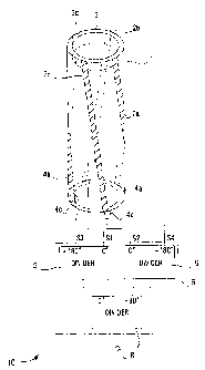
Figure 1 is a perspective view of a helical antenna 10
of a first embodiment according to the present invention;
Figure 2A is a perspective view of the upper part of a
dielectric cylinder 1 of the helical antenna 10 according to
the present invention, showing the cylindrical surface in one
plane;
Figure 2H is a view similar to Fig. 2A or another
embodiment of the upper part of the dielectric cylinder 1 of
the helical antenna 10 according to the present invention;
Figure 3 is a view similar to Fig. zA of the lower part
of the dielectric cylinder 1 of a helical antenna 10
according to the present invention;
Figure 4A is a view of a first shape of a feeder
conductor 4 of the helical antenna 20 according tv the
present invention;
Figure 4B is a view of a second shape of the feeder
conductor 4 0~ the helical antenna 10 according to the
present invention;
Figure 4C is a view of a third shape of the feeder
cvz~duc~tor 4 of the helical antenna 10 according to the
present invention;
Figure 4D is a view of a fourth shape of the feeder
conductor 4 of the helical antenna 10 according to the
- 5 -
CA 02232064 1998-03-13
present invention;
3~igure S is a perspective view of a helical antenna 20
of a aecond embodiment according to the present invention;
Figure 6 is a perspective view of a he3.ica1 antenna 30
of a third embodiment according to the present invention;
figure 7 is a perspective view of a helical antenna 7.00
according to prior art;
Figure 8 is a perspective view of an assembly procedure
o~ a helical antenna 100 according to prior azt;
Figure 9 is a perspective view of a metal conductor 106
of a helical antenna 200 according tv prior art; and
Figure 10 i$ a side view of another metal conductor 106
of a helzcal antenna 100 accozding to prior art.
DETAILED DESCRIPTION OF PREFERRED
EMBODTMENTS OF THE INVENTION
Several embodiments of the present invention will be
described with reference to the accompanying drawings.
Referring to Figure 1, a preferred embodiment of the
present invention is composed of a dielectric cylinder 7.;
tour zadiation conductors 2a, 2b, 2c, 2d arranged on the
outer surface of the dielectric cylinder 1; a matching
conductor 3 arranged on the upper inner surface of the
dielectric cylinder 7.; four feeder conductors 4a, 4b, 4c, 4d
arranged facing the radiation conductors 2a-2d; and a feeder
circui~~ 5 for feeding four high frequency signals to the
- 6 -
CA 02232064 1998-03-13
feeder conductors 4a, 4b, 4c, 4d with 90 degrees phase
difference from each other.
7:he operation of an antenna element according to the
present invention will be. described below with reference to
the drawings .
~=n Figure 1, there is an electrostatic capacitance
acros:~ the thickness of tie dielectric cylinder 1 between the
matching conductor 3 and the radiation conductors 2a-2d.
Therefore, both the matching conductor 3 and the radiation
cvnduc:tora 2a-2d are coupled with each other over a high
frequency range. 'that is, the radiation conductor 2a i$
effectively coupled not only with the matching conductor 3
but also with the radiation conductors 2b-2d in a high
frequency range. Therefore, even though the feeder impedance
of the radiation conductor 2a alone is high, such high feeder
impedance of the radiation Conductor 2a can be decreased by
adjusting the width and the position of the matching
conductor 3 and by adjusting the high freguency coupling
degree between them. As a result, an adeguate electrical
impedance matching can be~achieved.
The feeder conductors 4a~4d and the radiation conductors
2a-2d are .closely arranged on opposite sides of the
dielectric cylinder 1, so the feeder conductors 4a-4d and the
radiation conductors 2a-2d are coupled to each other by the
electrostatic capacitan,ce~ therebetween in a high frequency
range. In the conventiqnal helical antenna 100 shown in
Figure 7, the signal applied to the coaxial cable is directly
CA 02232064 1998-03-13
connected and directly fed to the helical conductors.
However, the helical antenna 10 according to the present
invention is coupled through high frequency, sv it is
possible to adjust the matching conditions with respect to
the radiation conductors 2a-2d by modifying the shape of the
feeder conductors 4a-4d.
Especially, if t:he radiation conductors 2a-2d have
inductive impedance, it is possible to attain the impedance
matching effectively by cancelling the feeder impedance.
'The operation of the feeder circuit 5 shown in Figure 1
is explained below.
:4 high frequency (normally microwave or quasi-microwave
frequency band) signal applied to a terminal 8 of feeder
circuit S is divided into four signals S1-S4 which have
phase;a offset from each other by 90 degrees and the same
amplitude by dividers ~, 7 and 9. The divided high frequency
signals S1-S4 are fed to the feeder conductors 4a-4d
reepec~tively. Such high frequency signals are fed to the
radiation conductors 2a-2d through the electrostatic coupling
between the feeder conductors 4a-4d and the radiation
conductors 2a~2d. The high frequency signals S1-S4 fed to
the radiation conductars 2a-2d radiate from the radiation
conducaors 2a-zd.
Details of the helical antenna 10 according to the
present invention will be described below with reference tv
FigurE: 1 through Figure 4.
I:n Figure 1, the dielectric cylinder 1 may be made of
- 8 -
CA 02232064 1998-03-13
plastic such as polycarbonate resin or acrylic zesin, as are
conventionally used.
The dielectric cylinder 1 may have an outer diameter
which is usually about o.la {~ is a wavelength of an
operating frequency). It is desirable that the thickness of
the dielectric cylinder 1 is about 0.01 or lees. In
addition, the length of the dielectric cylinder 1 is so
selected that it is shorter than about 1.5~, because such
length is effective to matching of a helical antenna having
a number of turns less than 2.
The radiation conductors 2 are arranged on the outer
surface of the dielectric cylinder 1 and are adhered tv the
dielectric cylinder Z by using a pressure sensitive adhesive
double coated tape. Desirable length of the radiation
conductors are about Z~ or less. If the length of the
radiation conductors 2 are the same as ~ or shorter, instead
of a. helical-shaped conductor, a straight rod-shaped
conductor yr a rod-shaped conductor which is straight but
folded at several points may be used.
The matching conductor 3 is arranged on the inner
surface of the dielectric cylinder 1.
Figure 2 shows a lvcational relation of the radiation
conductors 2, the dielectric cylinder 1 and the matching
conductor 3.
.As shown in Figure 2A, an impedance matching of the
helical antenna 10 is attained by adjusting a width w of the
matching conductor 3. Generally speaking, W is about
_ g _
CA 02232064 1998-03-13
0.01-0.1~. As shown in Figure 2B, the matching conductor 3
may be arranged offset from the end of the dielectric
cylinder 1 by a distance L1 if desired. A plurality of
matching conductors may also be arranged. L1 and L2 are
usually 0.2~ or shorter.
The feeder conductors 4 are arranged near the radiation
conductors 2 on the lower inner surface of the dielectric
cylinder ~.
Figure 3 shows a locational relation of the radiation
conductors 2, the dielectric cylinder 1 and the feeder
conductors 4. Similarly tv the matching conductor 3, the
feeder conductors 4 and the radiation conductors 2 axe
arranged with the dielectric cylinder 1 having thickness of
about 0.01x.
The feeder conductors 4 may take various shapes
accvr~ding tv the shape of the radiation conductors ae shown
t
in Fi<~ures 4A-4D. That is, as shown in Figure 4A, the feeder
condu~~tors 4 may take a rectangular shape. The feeder
conductors 4 may be arranged obliquely face to face with
respect to the radiation conductors 2. They may be arranged
in parallel with the radiation conductors 2, ae shown in
Figure 4B. They may be bent at a right angle, as shown in
Figure, 4C. They may take a slender rectangular shape, as
shown in Figure 4D.
2.5 As described above, it becomes possible to change the
electrostatic capacity and tv adjust matching conditions with
respect to the radiation conductors 2 by changing the shape
- io -
CA 02232064 1998-03-13
of the feeder conductors 4.
These feeder conductors 4a-4d are fed in phases
different by 90 degrees from each other from the feeder
circuit 5.
As shown in Figure 1, the feeder circuit 5 can be easily
composed by the divider 6 and 9 having phases different by
180 degrees from each ether and one divider 7 having a phase
different by 90 degrees from said two dividers.
The operation of the antenna element according to the
present invention will now be described.
In Figuz~e 1, the high frequency signal fed from the
terminal of feeder circuit a is divided into the signals
S1-84 having phases different by 90 degrees from each other
and the same amplitude by the dividers 7, 6 and 9. Such
divided signals S1-S4 are fed to the feeder conductors 4a-~d
respectively. Such signals axe also fed tv the radiation
condu~~tors 2a-2d through the electrostatic coupling between
the f~aeder conductors 4 and the radiation conductors 2.
'The high frequency signals 81-S4 fed tv the radiation
conductors 2a-2d are balanced signals and radiate from the
radiation conductors 2a-2d respectively. zn this case, to
radiate the high frequency signal efficiently from the
radiation conductor z , the output impedance of four terminals
of thc~ feeder circuit 5 must be equal to the input impedance
of sv~-called helical antenna respectively when the radiation
conductors 2 are viewed from the feeder conductors 4.
~3vwever, in the case of the helical antenna 10 having a
- 11 -
CA 02232064 1998-03-13
number of turns less than 2, the input impedance varies
greatly according to the length of the radiation conductors
2. Sometimes, the absolute value of the input impedance
varies over a range as wide as 30-2,000 ohmB.
To the contrary, the output impedance on the feeder
circuit 5 is usually about 30-3fl0 ohms, so it is necessary tv
match these impedancee with each other. In the case of the
antenna according to the present invention, such matching is
attained by means of the matching conductor 3 and the feeder
conductors 4, The coupling between the matching conductor 3
and the radiation conductors Z can be adjusted by modifying
the number and the position of the matching conductor 3. At
the same time, it is possible to adjust the absolute value of
the input impedance of the radiation conductors 2, namely,
the helical antenna itself.
'the matching conductor 3 is electrvstatically coupled
with the radiation canductors 2a-2d. For example, when
viewed from the radiation conductor 2a, the radiation
conductors 2b-2d are effectively coupled with each other
through the matching canductor 3. Therefore, even though the
single radiation conductor 2a has narrow or high feeding
impedance, such feeder impedance of the radiation conductor
2a can be made wider or lower by the addition of the matching
conductor 3, because the admittance Component is connected
2'~ equivalently in parallel by the matching conductor 3.
'.Che feeder conductors 4 are electrostatically coupled
with t:he radiation conductors 2. If the input impedance is
-- 12 -
CA 02232064 1998-03-13
such i~hat the radiation conductors 2 are inductive, impedance
matching can be attained by Canceling the reactance Component
by adjusting the degree of capacitive coupling.
In the above-mentioned embodiments, the feeder
conductors 4a-4d are arranged on the lower inner wall of the
diele~~tric cylinder 1, and the matching conductor is arranged
on th~~ upper inner wall thereof.
SECOND EMBODIMENT
~a
~~s shown in the perspective view of the helical antenna
20 of Figure 5, in the second embodiment of the present
invention, if electrical matching conditions can be
eatis:Eied, a configuration containing no matching conductor
3, that is, a configuration without the matching conductor 3
of Figure 1, may be used. The configuration shown in Figure
5 contains two radiation conductors 2a and 2b. This
confic~uratzon has the advantage that the construction of the
dielectric cylinder 1 can be simplified.'
2 IJ
THIRD EMBODIMENT
Tn the third embadiment, as shown in the perspective
view of the helical antenna 30 of Figure 6, the feeder
eonduc:tors 4a-4d are not electrostatically coupled with the
radiation conductors 2a-2d. They are directly coupled and
electrical matching is attained by means of the matching
_ ~3 _
CA 02232064 1998-03-13
conductor 3.
The configuration shown in Figure 1 contains four feeder
conductors ~ and four radiation conductors 2 and the feeder
conductors 4 are fed in phases different by 360/4=90 degrees
from each other.
However, the preeent invention is not limited to such
configuration. Generally, if any configuration contains n
(natural number more than 2) feedez conductors 4 and n
radiation conductors 2, electrical energy can be fed by
Shifting each phase of the feeder conductors 4 by (360/n)
degrees.
.As described above, in the case of the helical antenna
of the present invention,
(1) the matching conductor arranged on the inner wall of
the dielectric cylinder forming the helical antenna eguipped
with a plurality of the radiation conductors on its surface
has an advantage to lower the feeder impedance of the
radiation conductor.
(z) the feeder conductors arranged on the inner wall of
the dielectric cylinder forming the helical antenna equipped
with .a plurality of the radiation conductors an its surface
have an advantage to cancel the inductive reactance component
of the feeder impedance of the radiation conductor and to
lower the feeder impedance.
z5 'therefore, in the case of a small hel~.cal antenna
containing a short radiation conductor requiring broad fan
radiation for a portable terminal for the mobile satellite
- 14 -
CA 02232064 1998-03-13
communication and so on, due to the above-mentioned
advan~:.ages, very high impedance of the helical conductor can
be decreased, easy impedance matching becomes possible, VSWR
is improved, and transmission efficiency and antenna gain can
be enhanced.
t~7hile the present invention has been described in
connection with various preferred embodiments thereof, it is
to be expressly understood that these embodiments are not to
be construed in a limiting sense. Instead, numerous
modif:i.cationa and substitutions of equivalent structure and
techniques wi~.l be readily apparent to those skilled in this
art after reading the present application. All such
modifications and substitutions are considered to tall within
the true scope and spirit of the appended claims.
1 5
- 15 -