Note : Les descriptions sont présentées dans la langue officielle dans laquelle elles ont été soumises.
CA 02233069 1998-03-26
W O 97/124~7 1 PCT/SE96/01211
OPE~,ATION AND MAINTENANCE OF CLOCK DISTRIBUTION NETWORKS
HAVING REDUNDANCY
TECHNICAL FIELD
The present invention relates to distribution of a clock signal having redtlnd~ncy to a
suser of the signal and in particular methods and devices for m~int~n~nce of circuits for
distribution and of circuits for selecting a suitable clock signal. It also relates to networks or
~ in~t~ tionc having m~inten~nce functions provided therein. Further, it relates to a method
and a clock source for providing a clock signal having identific~tion information contained or
hidden therein. It relates also to a method and a device for proeeccing a elock signal to detect
o information contained therein. It relates to a method and a clock source for providing a clock
signal having intentional errors contained therein. It relates to a method and a device for
processing a clock signal in order to determine errors, in particular frequency and phase
errors, in a clock signal. Further, the invention also relates to supplying redundant clock
signals to c~cc~cled subsystems, i.e. subsystems connected to each other serially, the clock
5 signal passing through one subsystem where it is processed and then issued as a new clock
signal to a following subsystem, etc. It further relates to methods and devices for ev~lu~ting
two clock signals as to the timing of timing pulses in the clock signals in relation to each
other. The invention relates also to a method and a device for producing a pulse in~ ~ting a
signal sequence detected inside a clock signal. Finally, it relates to a method and a device for
20detecting a signal sequence contained or hidden in a clock signal.
BACKGROUND AND STATE OF THE ART
In the field of telephone connections and in telecommunication equipment generally, as a
rule there exists a need for distribution of two clocking signals, herein called clock and
synchronizing pulse rates, the latter one called "synch rate" in short, to various sub-
25 equipments and components therein. This distribution is particularly wide in physically largeconne~t~1 systems, such as in the type of switches having various multiplexing stages and
similar units. The clock rate has generally a high frequency and among other things defines
borders for bits in the data flowing through the equipment and the synch rate has a low
frequency and defines frame borders and similar things in the data signal. The number of
30 signals transferring clock and synch information in an equipment such as a
telecommuni~tion switch station can be rather large and in the following the general
e,~,es~ion "the clock distribution network" is used therefor. Telecommunic~tion equipment
in a m~g~7ine or cabinet, etc., has a considerable multitude of tr~ncmi~ion col.lpollents for
rate distribution in the shape of cables, pins in back planes and electrical leilllinals, lines in
35 back planes, etc. The space required for all such signal connections is con~i~P~hle and costs
money. As a rule, the number of pins in a connector is a small resource limiting the size of
for example a switch.
In equipments having large requirements of their reliability the clock distribution
network must of course also fulfil large reliability requirements. The reliability of the clock
40 distribution network can be enh~need, in the conventional way, by introducing redun~l~ncy.
If the clock distribution and the clock source are designed to include rednn(l~ncy, i.e. that
CA 02233069 1998-03-26
W O 97/124S7 2 PCT/SE96/01211
they may be duplicated or, as is supposed in the following herein, in the pl~rei,~d case
triplicated, a redundant and triplicated clocking structure can be m~int~ined from clocking
source to clocking receiver, however, in the receiver end one of the clocks must of course be
selected for operational use by the respective equipment.
5 In previous systems not having red~lnd~ncy, where clock rate and synch rate are to be
distributed to all m~g~ines and cabinets, as a rule two coaxial cable have been used to each
receiver or user of the rates, one coaxial cable for the high frequent clock rate and one cable
for the low frequency reference rate, that we call also the frame rate or the synch rate
herein.
o For distribution of clocking rates, where the high frequency clock is distributed
separated from the low frequency synch rate, the precision must be great so that for ex~mple
the pulses in the synch rate will not end up or be interpreted at the wrong one of the edges
of the clock rate pulses. This poses among other things great requirements on the similarity
of the lengths of the two cables used for clock and synch rate, respectively, in relation to
15 each other and also in relation to other pairs of cables having other destin~iQns in the
system.
Distribution of a clock signal which has a very high frequency and by means of which
circuits in telecommunication systems presently generally operate, in addition poses large
r~lirelllents on the ~hiPkling of cables and connectors, etc. together with good grounding
20 connections and similar things, so that inlel~,ence protection and functionality can be
provided and also maintained during a long time.
In for example large switches having circuits on circuit boards in n ~g~7ines and cabinets
there is thus a need for distributing a clock having a relatively high frequency and a rate
having a lower frequency as a reference for frame structures, etc. Clock rate and synch rate
25 can be distributed in the shape of a single, composite signal ("Composite Clock Signal"),
herein called CLSY (CLock and SYnch), as described in the International Patent Application
PCT/SE94/00321, which is incorporated herein by reference.
This signal comprises a clock frequency or clock rate that has a frequency considerably
lower than the real system frequency at which the circuits of the system operate, i.e. is
30advantageously an even fraction thereof such as 1/36 thereof, and it further comprises a
synch frequency or synch rate that is mod~ d on top of this clock frequency and
advantageously is an even fraction, such as 1/640, thereof.
A phase-locked loop circuit, PLL, is provided with logic circuits inte~ ing the synch
inl~ lation in the composite CLSY signal and it also generates a clock signal having a
35 frequency that is co~ erably higher than the clock frequency of the CLSY signal, such as
for example in a similar way as above, 36 times thereof. The PLL issues the synch pulse
with a precision in relation to the system clock that would have been very difficult to
produce using conventional clock distribution on two separate lines.
The advantages of distributing a frequency in the shape of CLSY, that has a con~idtor~hly
40 lower frequency colllpalc~d to the system clock and in addition is provided with synch
CA 02233069 1998-03-26
W O 97/12457 3 PCT/SE96/01211
information and of arranging for a PLL to generate the system clock rate together with synch
rate are:
1. The signal can be distributed more easily from an EMC point of view, i.e. in regard
of sensitivity to inle.rtlG.1ce from the outside and in regard of its own interfering iniluence.
5 The distribution m~Aillm must not have the same precision as in the case where system clock
~ and synch rate would have been distributed separately. This implies that for instance a single
~ optocable can be used.
2. Pins and space in connectors and back planes, etc. are saved by using the same
physical signal paths for both clock rate and synch rate.
3. A very good precision can be achieved by the arrangement that the PLL gçner~t~s
both the system clock and the synch on the same chip and from the same signal.
n-l~nt clock distribution systems are disclosed in the documents discussed briefly
hereinafter and also in other doc~lment~.
In the J~p~nese Patent Application JP-A 60-225982 clock pulse synchronization isdescribed in a triplicated system. A harmful influence of errors is prevented by correction by
means of majority decisions.
In U.S. Patent US-A 4,185,245 an arrangement is described for fault-tolerant clock
signal distribution. First and second redundant clock signal sources are arranged. Clock
rece*ers include sequential logic circuits for eY~mining the two clock signals in order to
20 ignore the clock signal pulse train that comes after the other one as to the phases thereof.
U.S. Patent US-A 4,489,412 discloses a network comprising supply of clock and
synchronizing signals by means of clock distribution modules that pe-ror-,- majority voting
for output signals from three oscillators.
U.S. Patent US-A 4,692,932 is related to triplicated clock distribution, each clock signal
25 including a synchronizing signal. In the receivers R logic circuits for majority voting are
incl~lded comprising three AND-gates and one NOR-gate in each receiver. These majority
circuits pass only the input clock signal that has a phase position located between those of the
other two clock signals. No tests are made of the quality of the received clock signals in the
receivers in order to make the selection.
In U.S. Patent US-A 4,698,826 triplicated clock distribution is described. Each clock
outputs a signal including a clock signal and a synchronizing signal.
U.S. Patent US-A 5,065,454 discloses a clock signal distribution arrangement having
redun-1~nt clock generation. The distribution paths are duplicated for redundancy reasons.
The European Patent Application EP-A2 0 365 819 treats the problem of synchronizing
35 the individual clocks in a mul~ ocessor system. A number of clock sources have each one
its PLL circuit, see column 10, lines 31 - 58. The clocks transmit reference signals to each
other which are subjected to a selection operation in each clock.
~ The European Patent Application EP-A2 0 366 326 treats the problem of en~--ring, in a
colllpu~ system in which a number of clock signals are derived from a main oscillator
40 signal, that the clock signals appear at the right times where they are needed. It l~Uil~S the
introduction of a small time delay between the clock signals in order to compensate for
CA 02233069 1998-03-26
W O 97/12457 4 PCT/SE96/01211
dirrere~tly long tr~nsmi~sinn paths. The solution described aims at re~ucing the risk of errors
in the time delays of the different clock signals. A PLL circuit is used for ...zti"t~ining a
phase relationship between each clock signal and a reference clock signal.
In U.S. Patent Docum~nt US-A 4,239,982 a fault-tolerant clock system is disclosed that
5iS intendecl to produce system clock signals by means of several clock sources. Each clock
source receives as input signals the clock signals generated from all other clock sources and
contains receiver circuits for deriving a system clock signal from these clock sources. Each
clock source generates and distributes to the other clock sources a clock signal that is locked
in phase to the system clock derived from its clock receiver. The system allows the use of
ohigh clock frequencies comprising a minimum phase jitter between derived system clock
signals.
In the European Patent Application EP-A2 0 303 916 four rate signals that are
synchronous as to frequency and phase are generated, for providing timing for e.g. a
computer system. The generation of the rate signals is made by means of four PLLs, the
5 output signals of which are fed to four selector circuits, in which a type of majority voting is
performed. The signal selected by a selector circuit is fed back to a definite one of the rate
generators for controlling it. Delay circuits are introduced for adapting the phase position of
the selected signals. Such delays cannot easily be introduced in the case where the clock
signal contains both a clock and a synchronizing rate, the latter one having a low frequency.
In U.S. Patent US-A 4,105,900 a triplicated control system is disclosed in which three
redundant sensor signals are used, one of these signals providing precise information and the
rem~ining two ones less precise information. A selection of signal according to a pre-
programmed priority order is based on the operative state of the three sensors.
SUMMARY
It is an object of the invention to provide methods and networks or installations using a
clock signal distribution system fulfilling the requirements that can be posed on the clock
functions in a switch having a redun~ tnt structure, in particular in systems that demand a
system clock signal having a high or very high frequency and a synchronizing clock signal
having a low frequency.
It is a further object of the invention to provide a redundant clock signal distribution
system that allows a simple caCc~e~l communication of clock signals between each sub-
system, so that short conductor paths are obtained.
It is a further object of the invention to provide a clock signal distribution system that
has a high MTBSF (Mean Time Between System Failure).
It is a further object of the invention to provide a clock signal distribution system in
which errors can be dete~ted in an efficient way both in clock signals and in various circuits
used for distributing, proc~ing and sele~ting clock signals.
It is a further object of the invention to provide various methods and devices that in an
advantageous way allow an efficient supervision of lines and circuits in a clock signal
40 distribution system.
CA 02233069 1998-03-26
W O 97/124~7 5 PCT/SE96/01211
The problem that is solved by the invention is thus to provide m~thsrl~ and
networks/in~t~ ti-~ns and various devices and metho~s needed therein for an effi(~iPnt
distribution of clock signals to subsystems or subordinate stations, the distribution allowing
the signals, lines and circuits used to be tested for errors all the time.
l~iun~i~ncy of an electronic system, such as a switch for telecomm-lnic~tion, and of the
clock functions thereof, is in the conventional way achieved by triplicating all hardware, i.e.
circuits, connection lines, etc. This method of increasing MTBSF thus comprises that several
id~o-ntir~l units, planes are provided that each one alone can ~ rO~I~l the required operation or
~Y~ute the lc~luired ~ ,cesses in parallel. By comp~rin~ the output signals from the three
10 planes, a plane having an error can be i(lentifie~. By excluding that plane that differs from
the other ones and having those planes that are similar "decide", a faulty plane can be
eYçluded. This method is called majority voting. In order that a triplicated system based on
majority voting is to work it is required that the majority voting works in a meaningful way,
i.e. the number of operative planes must be larger than the number of faulty planes. If all the
15 three planes in a triplicated system are correct, the system can be said to work and have a
full red--n-l~ncy. If one of the planes is faulty, the switch can be said to still work but
without any redundancy.
What makes the "mean time up to system failure" (MTBSF) for a triplicated systemhigher, is that it is understood that in the case where one of the planes breaks down, it must
20 be replaced within some rather short time, for example within one week, so that no further
error will have time to appear during the critical time when the system has no redundancy. If
another one of the planes would break down before the plane first being faulty has been
ten-le~ to, the system will stop to work completely.
It can be observed that the mean time between errors in a triplicated system is at least
25 three times shorter (= worse) than in a single, non-triplicated, system since it contains at
least three times of the amount of hardware compared to the corresponding non-triplicated
system. However, still the mean time between system failure, i.e. the time that is to pass
before the function of the triplicated system stops, is increased since two faults in two
dirre~ t planes are required simultaneously in order that the function of the triplicated
30 system will cease.
If a plane in a triplicated system stops to work, it is not noticed in the functionality on a
system level, since the triplicated system continues to work but without any re~--n-l~ncy. In
order that the tril)lic~t~d system is to obtain an improved MTBSF it is important that all
faults are discovered. If a fault arises and if this fault is not dete~ted, it is called a hidden
35 fault. A triplicated system cont~inin~ hidden faults can work but with a reduced rednnrl~ney.
A system that can contain hidden faults will have a worse MTBSF.
In order to obtain a high MTBSF it is thus important to arrange for a good faultdetectic-n in the system, i.e. that the number of possible hidden faults should be as low as
possible. In order to achieve this it is in turn nerçc~.y to introduce extra tests in the system,
40 here called m~inten~nce tests. All hardware can break down, also hardware being incl~ldecl in
the majority voting. All alarm signals can be non-operative, so that they signal "no alarm",
CA 02233069 1998-03-26
W O 97/12457 6 PCT/SE96/01211
though in reality an alarm situation exists. All signals that are static (= constant or has a
constant logical or electrical level) or stationary can be non-operative without this state being
noticed.
A reliable indic~ion of the fact whether a plane is faulty or correct is thus something
5 more than the mere presence of a static signal in the hardware. A method used for testing the
clock function is that continuously a predetermined number of artificial faults are introduced
and that a check is made all the time that the corresponding number of faults has been
detected.
To snmm~rize, it can be said that in the redundant system that has a MTBSF that is as
o high as possible, possible hidden faults are highly reduced and in the system, as described
hereinafter, in order to detect possible faults to as large an extent as possible a method is
used based on maintenance tests, where thus artificial errors are introduced in the system in
order to check whether the system is capable of detecting them. If all artificial faults are
detected the system is correct but otherwise, if they are not detected, at least one error exists
15 in the system.
Generally thus, a clock signal is distributed in an electronic system such as some type of
network or electronic in~t~ tion, for example for processing information, for performing
processes in different stations or for comm~niC~ting information between stations, the clock
signal being used for control of various devices, processes, etc. in the system. The clock
20signal for different subsystems in an electronic system is provided in such a way that the
clock signal is delivered or communicated on at least three different, independent lines or
ch~nnelc to such a subsystem. The subsystem performs, as is previously known, a selection
of one clock signal among the signals received on the different lines or ch~nnel~ The
original clock signal or the clock signal arriving to a subsystem is always generated
25 independently by this subsystem and thus independently of circuits and processes therein and
of the output signals or results thelerloll~. In the subsystem then, the selection of a clock
signal is pt;l rOl Illed independently and in parallel by or in at least two different, in the
normal case three, selection processes working independently of each other, such as in or by
at least two different selector units working independently of each other, for producing at
30 least two selected clock signals and in the preferred case three selected outgoing or useful
clock signals. The selected clock signals can of course be identical at each time instant,
supplied on the same line or ch~nnel. These selected clock signals are used in reduntl~nt
planes in the subsystem and for a c~c~ded distribution to another subsystem, theconstruction and operation of which as to the production of such selected clock signals are
35 iclentic~l to the subsystem first mentioned. The sPlected~ at least two clock ~ign~l~, are then
allowed to pass to the devices or processes in the subsystem or to another subsystem,
essentially unaltered or unaffected by the selection process. This is accomplished by
providing the received clock signals to switches in the subsystem where these switches are
controlled by the at least two selection processes. When required or desired a change to a
40 new one or another of the received clock signals can be made and this new or another clock
is instead passed to the devices or processes or subsystem.
CA 02233069 1998-03-26
W O 97/12457 7 PCT/SE96/01211
The selection processes work intelligently. They thus evaluate all the received clock
signals in regard of their quality or characteristics and determine therefrom the clock signal
to be sçlect~A by providing a signal to a switch.
The arriving clock signal can advantageously consist of at least three different signals
that are delivered or communic~t~d to a subsystem from at least three different clock
sources, that each one generates a subst~nti~lly identi~l clock signal or a clock signal that
- has subst~nti~lly the same timing information. The clock sources can in principle work
inflepen~l~.ntly of each other and they can also, in the case where they are the original clock
sources in a system, receive common information for establishing the phase position of
o synchronizing rate information having a low frequency, this information then being included
in the clock signal provided by a clock source.
Advantageously the number of different independent processes or selector units for
selection of clock signals in a subsystem is equal to the number of independent lines or
ch~nnel~, on which the clock signal arrives to the subsystem, this number preferably being
equal to three.
In such a process or in a selector unit, in the selection of a clock signal, all signals can
be evaluated that are received from the at least three different lines or channels which arrive
to a subsystem, as to faults or errors in the frequencies of the signals and/or in the phase
position of a clock signal in relation to the phase position of the other received clock signals.
20 This evaluation is then made independently by or in the different processes or in the different
selector units.
Por evaluating received signals, faults or errors in each such signal received on the
different lines or ch~nnel~ can be determined, the number of errors be counted and further,
the number of counted errors in each such clock signal can be evaluated for establishing
25 whether such a clock signal is faulty and/or whether some process or circuit used in
generating, tr~nsmitting, receiving and also evaluating or selecting a clock signal is faulty.
Some error frequency can actually be normal, as will appear hereinafter.
In the case where different clock sources are used or else in tr~ncmi~sion devices
provided at the independent transmission lines or channels, advantageously intentional errors
30 are introduced in the clock signals and these errors are introduced in such a way that the
different processes or selector units for selection of a signal in the subsystem will all the time
change to a new selected signal. This presupposes that there exists at least two signals among
which the selection is made, i.e. that at least two signals in each moment are judged to be or
are determined to have a good quality and then e.g. be as free from errors as required or as
35 possible. An average phase position of the selecte~ and switched signal will then be obtained,
that for example will give a reduced phase jump, in the case where one of the signals is
determined to be faulty and will not be comprised any longer in the repeated change of a
- select~i signal.
The errors in the clock signals are preferably introduced in such a way that the different
40 selection processes or selector units cyclically and/or in a way regular in time change to a
new selected signal. In the latter case it is intended that if for example three signals A, B, C
,
CA 02233069 1998-03-26
W O 97/12457 8 PCT/SE96/01211
are available a change from A to B is made after a first predetermined time period, a change
from B to C after a second predetermined time period and a change from C to A after a third
predetermined time period.
Errors that have been determined in a received signal, can also be evaluated by the
5 method that for example type of detected error and possibly the time of the appearance
thereof are stored in some memory means arranged therefor, so that a sequence of such
errors will be used in an evaluation algorithm. Such an algorithm could also be executed in a
state m~hine and then no direct memory means are required for storing a sequence of
cletected errors.
10 In the case where intentionally introduced errors exist in the clock signals and then
changes of selected signal are constantly made in one of the independent processes or
selector units, also the number of time when a new clock signal is selected or a switch unit
switches to let another clock signal pass can be determined and/or evaluated, or a sequence
of such new selections or changes and possibly the times thereof can be evaluated in a
similar way as has been described above for evaluating errors detected in the signals.
For among other purposes a simple counting of such changes, in the generation of each
clock signal information can be introduced therein indicating the identity of the clock signal
and thereby also the identity of the clock source generating the clock signal. Then in a sub-
system, in a process for selection of a signal or in a selector unit, the selected signal can be
20 monitored in regard of such identity information, and when such information is dete~ted, the
arriving clock signal or the clock source, to which the information belongs or points, is
determined. The number of times is counted that information pointing to each individual
arriving clock signal is found and such counted numbers are evaluated. Alternatively such
information for a sequence of new selections or changes, as related to a received clock signal
25 or to a clock source can be evaluated in a way similar to that described above with reference
to evaluation of errors. Also the times when the information has been determined can like
above be used in such an evaluation.
In the introduction of intentional errors or of identity information it is naturally ~sllmed
that each received clock signal is generated as a sequence of pulses from which timing
30 information can be derived. Such a pulse sequence will then substantially agree with a pulse
sequence chosen as a main template, for example of the composite clock signal type
described in the International Patent Application PCT/SE94/00321 cited above. Such a pulse
sequence contains a regular sequence of pulses interrupted by especially designed but
iderlti~l short sections forming the synchloni~ing rate pulse. The main template pulse train
35can naturally have a different design, such as con~i~ting of a repeated sequence of one or
more pulse bursts having a constant level therebetween and/or therebefore and/or thereafter.
Generally each pulse comprises in the conventional way a first transition from a first level to
a second level and a second transition from the second level to the first level, so that the
template pulse train will comprise a sequence or train of such transitions.
For introducing identity information in such a clock signal the clock signal is generated
so that it agrees with the main template pulse train but within at least one predetermined
CA 02233069 1998-03-26
W O 97/12457 9 PCT/SE96/01211
section, within which the clock signal instead agrees with an identity template pulse train,
which co.l~;~onds to a deformed section of the main template pulse train.
In the case where all of the main template pulse train is periodic, what naturally is the
normal case, it thus comprises a fixed template pulse subtrain repeated with a definite time
5 period. The clock signal is then generated advantageously so that the predetermined section
- that has a lacking agreement with the main template pulse train has a fixed position in time
within each period of the main template pulse train.
In the introduction of identity information the clock signal can also be generated so that
it coincides with the main template pulse train except that at least one pulse Ihaving a
0predetermined position in the main template pulse train is omitted, in particular having a
predetermined position and then a fixed time position in a periodically repeated template
pulse subtrain.
For introducing identity information the clock signal can further be generated so that it
agrees with the main template pulse train except that at least one transition having a
15 predetermined position in the main template pulse train is changed, in particular that a
transition having a predetermined position is omitted and that a transition of a kind opposite
to the omitted transition and having a predetermined position is changed to the kind to which
the omitted transition belongs.
For intentionally introducing a frequency error a clock signal can be generated so that it
20 agrees with the main template pulse train except that a first predetermined number of
s~lc-cçccive pulses are omitted. In order to intentionally introduce or imitate a phase fault in
the corresponding way a clock signal can be generated so that it agrees with the main
template pulse train except that a second predetermined number of successive pulses are
omitted. The second predetermined number should then be greater than the first pre-
25 determined number, so that an intentionally introduced phase error is also a frequency errorand thus when det~cting an error and determining that it is a phase error, this error will be
determined to also be a frequency error. However, a correct determination of the kind of
encountered error can still be made, owing to that a detected frequency error will not
necess~.ily be determined to be a phase error.
In detecting errors in clock signals as considered in relation to each other and in
particular in determining whether timing pulses have timing errors in relation to each other,
n~t~ lly in a known way a simple AND-gate can be used for an in~iç~tion of the time
position. However, it will provide a rough Çctim~tion and instead, in order to obtain a
determination the accuracy of which easily can be set, a method can be used utili7ing a fixed
35 pulse signal having pulses of a frequency that is considerably higher than the frequency of
the timing pulses in the clock signals. By means of the high frequency signal from each
timing pulse an evaluation pulse is formed that starts at the same time as the timing pulse but
has an end that is determined by the start of a pulse in the fixed pulse signal, so that the
evaluation pulse will have a length forming a predetermined number of periods of the fixed
40 pulse signal and a fraction of such a period. Then, an AND-operation is made on the
evaluation pulses thus prod~lced, i.e. an intersection pulse is produced being conctitllted by
CA 02233069 1998-03-26
W O 97/12457 lO PCT/SE96/01211
the intersection of the evaluation pulses. An alarm signal signifying a timing error between
the clock signals is then provided when the intersection is empty, i.e. in the case where the
inle~ ion pulse is not there.
Such a detection can also be made to include hysteresis. By means of the fixed pulse
5 signal having a high frequency in the same way, from each timing pulse a first evaluation
pulse is formed that starts at the same time as the timing pulse but has an end that is
determined of the start of a pulse in the fixed pulse signal, so that the first evaluation pulse
will have a length conctituting a first predetermined number of periods of the fixed pulse
signal and a fraction of such a period. In the corresponding way a second evaluation pulse is
o formed that has a length conctit~lting a second predetermined number of periods of the fixed
pulse signal and a fraction of such a period. The second predetermined number is not equal
to the first predetermined number but is preferably greater than it. First and second
intersection pulses are produced from the intersection of the first and the second evaluation
pulses, respectively. The time intervals between the appearance of, i.e. for example the start
15 of, the first intersection pulses are monitored and a first signal is provided in the case where
this time interval is larger than a threshold value. The time intervals between the appearances
of the second intersection pulses are similarly monitored and a second signal is provided in
the case where this time interval is larger than the same threshold value. An alarm signal
signifying a timing error between the clock signals will then not be produced until the second
20 signal appears and the production of this alarm signal will not end until a transition of the
first signal that is such that this signal continues from an existent state to a non-existent state.
This will give a hysteresis of a magnitude corresponding to the difference of the second and
first predetermined numbers of pulses.
In the composite clock signal there is, as has been mentioned above, a base band clock
25 having a base frequency comprising in principle, substantially regularly repeated similar
pulses and signal sequences, that among other things indicate a synch pulse and that
correspond to deformed short sections of the base band clock. In the detection of a synch
pulse or a synch pattern a pulse is obtained as an output signal that has not a completely
definite time position in relation to such an encountered pattern, owing to tolerances of the
30 electronic co~ onents used. Then a pulse in the base band clock can be extracted and
isolated at a definitP ~ t~nce in time from the synch pattern, what is made in the following
manner. A signal sequence such as a synch pattern is thus dete~t~d by some suitable detector
that is arranged to generate a first pulse. This pulse will naturally appear after the detection
of a signal se~uence and it will have a suitably, accurately chosen position in time that is
35 generally easy to accomplish using conventional components. The time position must be such
that a ~lefinitP tr~n~ition in the first pulse, for example its first edge is always Citl-~tçd within t
a time interval that is shorter than a space between pulses in the base band clock signal of the
clock pulse signal. From the first pulse, in a delay and pulse shaping circuit a second pulse is
produced starting after the other pulse having a predetermined delay and having a length that
40iS shorter than one period time of the base band clock of the clock pulse signal, so that the
second pulse will appear in time at the same time as the whole time length of a complete
CA 02233069 1998-03-26
W O 97/124S7 11 PCT/SE96/01211
clock pulse of the base frequency in the clock pulse signal. Finally, in an AND-gate the
intersection of the second pulse and the clock pulse signal is formed, whereby, on an output
terminal of the gate, the whole clock pulse will be provided as one isolated pulse.
In the dçt~cti~.n of a signal sequence a detector can be used that inçludes a source of an
5 auxiliary clock pulse signal having generally a considerably higher frequency than the clock
- pulse signa'l. The source can work independently of the clock pulse signal and provide pulses
having a frequency, say 4 to 10 times of the base band frequency thereof. The clock pulse
signal is sampled by means of the auxiliary clock pulse signal and the pattern of the sampled
signal is evaluated by a comparison to one or several predetermined patterns, and at
10 agreement the first pulse is produced.
For the sampling a shift register can be used and the high frequency pulse signal is then
provided to the clock input terminal of the shift register. To the shift input terminal thereof
the clock pulse signal is delivered. The shift positions of the shih register are connected to a
suitable combinatorial network so that the first pulse is obtained on the output terminal of the
15 network. The m~nitude of the shift register must be chosen based on the length of the signal
sequence and the ratio of the frequency of the pulse signal generated by the source and the
base band frequency of the clock pulse signal. The frequency of the auxiliary clock signal
should not be too high, since a too high frequency will imply that a large shift register must
be used and that the combinatorial network will be large and complicated. A too low
20 frequency of the auxiliary clock signal can provide a too bad signal pattern recognition.
BRIEF DESCRIPTION OF THE DRAWINGS
The invention will now be described as a non-limiting exemplary embodiment with
reference to the accompanying drawings in which
- Fig. 1 is a block diagram of a clock distribution system,
- Fig. 2 is a diagram illustrating the structure of a frame in a clock signal,
- Fig. 3 are wave form diagrams as functions of time that illustrate various subsequences
of the clock signal frame,
- Fig. 4 is a block diagram of a clock selector unit,
- Fig. 5a is a block diagram of a frequency error detector,
- Fig. Sb is a wave form diagram of a section of a composite clock signal containing a
synch sequence,
- Figs. 5c - Se are wave form diagrams of output signals from various circuits
illllst~.~ting how an isolation of a synch pulse is made,
- Fig. 6a is a block diagram of a phase error detector,
- Fig. 6b is a block diagram of a differentiation circuit used in the phase error clçtt?ct r,
- Figs. 6c - 6e are wave form diagrams illustrating the signal processing in thedirrelGIltiation circuit,
- - Fig. 6f is a block diagram of a coincidence detector used in the phase error dçtector,
- Figs. 6g - i are wave form diagrams illustrating the signal processing in the
40 coinci~çnce detector,
,
CA 02233069 1998-03-26
W O 97/12457 12 PCT~,E96/01211
- Fig. 6j is a block diagram of a time interval monitoring unit used in the phase error
detector,
- Fig. 6k is a state diagram of a hysteresis circuit used in the phase error detector,
- Fig. 61 is a time diagram illustrating the states of the hysteresis circuit,
- Fig. 6m is a block diagram illustrating how phase errors are monitored,
- Figs. 6n and 6O are wave form diagrams illustrating the function of a hold circuit,
- Fig. 7a is a block diagram of a clock selector control,
- Fig. 7b is a truth table of a combinatorial circuit used in the clock selector control,
- Fig. 7c is a state diagram of a state machine used in the clock selector control,
lO - Fig. 8 is a schematic block diagram of a unit for selecting a clock signal and for
producing a system clock and a synch rate.
DETAILED DESCRIPTION
The following detailed description is based on a clocking signal called CLSY (CLock
and SYnch signal), see the discussion above and the International Patent Application
15 PCT/SE94/00321 mentioned above.
The CLSY signal is a composite clock signal that is composed of a clock signal "clock"
which hereinafter is assumed to be chosen to 5.12 MHz and is a pulse signal, typically a
square wave signal, having a frequency that is here called the base frequency or the base
band frequency, and a synchronizing signal "synch" having a frequency that hereinafter is
20~cllmed to be chosen to 8 kHz. The clock frequency that is supposed to be used in the
system of the different "useful components" thereof is 184.32 MHz and is also called the
frequency of the system bit clock or the frequency of the system clock, but in order to be
able to distribute more easily clock rates in the system the clock rate is distributed in this
way having a lower frequency, the base band frequency in order to be, on the receiver side,
25 i.e. in each unit that needs a system rate, multiplied by a factor of 36 in a PLL, a phase-
locked loop circuit, in order to obtain the desired system clock of 184.32 MHz. The PLL
also decodes the synchronizing signal that is included in the CLSY signal. The PLL has also
the quality of being insensitive to the cases where single pulses in the input signal are
omitted or where there are single spikes in the input signal.
Inside the CLSY signals codes for maintenance testing are also provided. These codes or
p~ttPrn~ supply information in regard of the plane in which a considered CLSY signal is
generated and further, they emulate certain errors for m~inten~nce testing the hardware.
There are several advantages of the CLSY signal, as has been indicated above: phase
differences between clock rate and synch rate are reduced, the number of physical signal
35 conductors is reduced and "phase jumps" will have m~gnitudes of at most 1/4 of the period
of the synch and clock rate respectively, i.e. of the periods corresponding to the frequencies
of 8 kHz and 5.12 MHz respectively.
The logical alchilG~;lulG of the generation, distribution and termination of the clock and
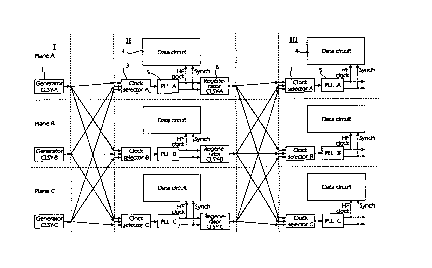
synch signal will first be described at a general level. In Fig. 1 it is shown in principle, how
40 three gPnPr~t~rs 1 create the composite clock signals, the CLSY signals, i.e. three equivalent
composite signals here called CLSY-A, CLSY-B, CLSY-C, that contain both a clock rate
CA 02233069 1998-03-26
W O 97/12457 13 PCT/SE96/01211
and a synch rate. These composite clock signals are distributed from each generator 1 to
each one of three clock selectors 3 that terminate the triplicated distribution. In each such
clock selector 3 an independent choice is made, independent of the other two clock selectors,
of the "best" clock signal by ev~ ting the different received clock signals and comparisons
~ thereof. Thereafter the selçctçd CLSY signal passes from each clock selector 3 to a following
~ phase-locked loop circuit 5, PLL, in order to be separated there in its components, the clock
rate and the synch rate, respectively, and for generating a system bit clock. The system bit
clock and the synch rate are used in each plane by various electronic circuits that are
sch~m~tic~lly illustrated by the triplicated data circuit 4 in Fig. 1.
lO Each one of the oscill~tors 1 is constructed so that it creates a composite clock signal, a
CLSY signal, containing pulses or pulse patterns for definition of clock rate and synch rate
and further also sequences of pulses or changed or modified pulses that imitate errors, for
m~int~n~nce testing following clock selectors 3, and also, hidden in the pattern of pulses for
clock rate and synch rate, by the method that some pulses have been changed, an identity
1scode comprising information on the plane in which the considered CLSY signal has been
generated, i.e. whether it has been generated by the oscillator in plane A, B or C. "Artificial
errors" in the CLSY signal are created by the method that a CLSY generator I introduces the
errors in the composite clock signal already from the beginning, so that the errors constitute
a natural part of the CLSY signal. By this method it will not be possible to remove or add
20 artificial errors on comm~nd.
The task for a clock selector 3 is to autonomously select a working composite clock
signal among the three arriving clock signals CLSY-A, CLSY-B, CLSY-C. Criteria of the
fact that a CLSY signal is to be considered as correct is that its frequency is correct and that
its phase position in relation to the two other CLSY signals is to be located within certain
25 limits. The clock selector 3 thus makes an autonomous judgement of the frequency and the
phase position in relation to each other of the arriving clock signals and selects according to
an algorithm one of the input signals, which is communicated to the output terminal of the
clock selector 3 through a multiplexer in the clock selector 3. The clock selector is thus
m~intçn~ncç tested by means of artificial errors which are always included in the CLSY
30 signals. Further, the artificial errors are entered so that the clock selector 3 will run through
all accepted clock signals and in particular so that it periodically and in a pattern that is
regular in time changes cyclically between them. In this way it is constantly verified that it is
possible for a clock selector 3 to actually select anyone of all accepted composite clock
signals. By using this method no signals are to be provided that are outside the functional
35 clock distribution, but the signals needed for the maintenance testing are always incorporated
as a part of the functional clock signal.
The function of a PLL 5 is, as has been mentioned above, to separate the arriving CLSY
signal in its components, signals for clock and synch rate respectively, to multiply the
e~tr~cted clock frequency to the system bit frequency of 184.32 MHz, to filter out ID-codes
40 and emulated, i.e. intentionally introduced, error patterns, to convert abrupt phase jumps to
slow phase drifts and to filter jitter that can exist in the input signal to the PLL 5.
CA 02233069 1998-03-26
W O 97/12457 14 PCT/SE96/01211
In order to obtain a high MTBSF (Mean Time Between System Failure) for the circuits
and connections in the system, it is important that as many as possible of the possible errors
that can arise in the hardware can be safely detected. It is also important that a possibility
exists of loc~li7ing an error as well as it is important that no errors are prop~t~d through
5 the system and thereby give the system worse characteristics.
In order to obtain this, it is naturally important that the mainten~nce functions are as
reliable as possible. Further, if a hardware error would appear in the very m~inten~nce
functions, this should also be possible to detect wherever the error has arisen. Similarly, the
design of the system should not be such that an error actually has arisen in some part that
o influences the main task of the system and that the maintenance functions are not capable of
detecting this error owing to some error in the maintenance functions or some other error or
owing to an imperfect construction.
To use a single static hardware signal, that informs on alarm state, thus "OK" or "not
OK", must be considered as unreliable, as has been mentioned above. A hardware error can
5 have arisen in the hardware communicating the signal, so that the information of the signal is
erroneous. It can indicate "error" even if it is "OK", or indicate "OK" in spite of being
"error" .
In the design of maintenance systems for clock functions the principle is used that at least
two different signals in the hardware are to be supervised by software and the criterion of the
20 fact that the system is to be judged correct should be that there must exist a certain relation
between these hardware signals and further, that the hardware signals should not be static,
but that they instead should be constituted by either counters or flags, which change
according to a predetermined pattern, for example such as that a certain flag is set at some
occasion and then is reset at another occasion. The software should then require that the
25 expected dynamics, i.e. the serial order in which the flag is set and reset ,~ecLively, exists
all the time and that otherwise an alarm signal is generated in the software.
The function of a clock selector 3 is according to the discussion above mainly both to
select away, at each time instance, a badly working clock and to select among the remaining
correct clock signals a working clock signal CLSY-A, CLSY-B or CLSY-C. In order to
30 check whether a clock selector 3 is working, that clock signal which at a considered time
instant is se-lected by the considered clock selector 3, is deteriorated by the permanently and
intentionally introduced errors, and supervising functions check that the clock selector 3 then
is capable of sele~tinf~ another composite clock signal.
The clock signals, the CLSY signals, are therefor, as has been in-iic~ted above, made to
35 contain, already from the start, pulse sequences which imitate defective clock signals. The
CLSY signals are generated in the construction blocks that are called CLSY generators 1 in
Fig. 1. The artificial errors which are found in a CLSY signal are further entered so that
they correspond to criteria that define the clock qualities which the clock selector is to accept
or not accept, respectively.
From a clock selector 3 the selected CLSY signal is provided and in order to be able to
decide if it is that CLSY signal that the system should select or think that it has selecte~, the
CA 02233069 1998-03-26
W O 97/12457 15 PCT/SE96/01211
CLSY signals have, according to the ~iscus~ion above, also been provided with identity
codes, ID-codes, during the generation of the signal. The CLSY signal that is generated in
the A plane, is thus called CLSY-A and is provided with an identity code A, indicating that
the CLSY signal has its origin in the A plane. In the corresponding way the CLSY signal
5 from the B plane is provided with an ID-B code and the CLSY signal from the C plane with
a code for C. By monitoring the CLSY signal provided from a clock selector 3 superior
filnctionc in the system can determine the identity of the CLSY signal that has been selected.
A CLSY signal is divided into frames which each one has a length of 125 microseconds,
i.e. the frames are repeated with the frequency 8 kHz which is the same as the synch rate,
o and they comprise 640 cycles or periods of the clock rate signal of 5.12 MHz. Further each
pulse or period of the clock rate signal can be considered as two halfperiods, where a
transition, positive or negative, can occur, and using this way of looking then 1280 data bits
exist in each CLSY frame. These bits are numbered from 1 up to 1280 as is shown in Fig.
2. A CLSY frame is divided into 8 subframes and each subframe is divided into three sub-
15SeCtiOnC, the first and second subsections of which each one has a length of 54 bits and thethird subsection of which has a length of 52 bits.
In the beginning of each CLSY frame a pattern is provided for frame recognition and
this pattern is called a synchronization pattern or synchronization sequence that in-lic~tes a
synch pulse. It is this pattern that a PLL 5 recognizes and each time that this pattern is
20 recognized by a PLL 5, the PLL 5 generates a corresponding synchronization pulse. This
synchronization pattern increments, for each time that it appears on the output of the
multiplexer of the clock selector, a counter for synchronization patterns as will be described
hereinafter.
In each CLSY frame two ID-codes are arranged, naturally denoting the same plane. In
25 the CLSY signal generated in the A plane two ID-codes for A are provided. Thecorresponding condition applies to CLSY signals generated in the B and C planes.In Fig. 3 subsequences of the CLSY frame that are schematically illustrated in Fig. 2 are
shown as wave form diagrams. The numbers within squares in these figures correspond to
each other. In the CLSY signals particular bit sequences or pulse sections of the pulses in the
30 base band frequency are arranged that indicate synchronization pulses S for each frame,
frequency reject sequences F, phase reject frequencies P and identity codes ID-A, ID-B, ID-
C. Each frame thus starts with a synchronization sequence S. Within each subsection of a
frame there is an intention~lly introduced error sequence F or P for simulating frequency
errors and phase errors respectively in a single one of the three clock cign~lc The flict~n~e
35 from a frequency reject sequence F to the following border between two subsections in the
frarne is always constant. The distance from a phase reject sequence to the most nearly
located, following border between subsections is also constant but has a value which is
~ different from the distance that applies to the frequency reject sequences and which in
particular is less than it. The ID-codes ID-A, ID-B, ID-C always follow directly after a
40 border between two subsections, i.e. they arrive first or early in a subsection, before the
error sequence therein. The error sequences F or P always follow in the later part of a sub-
CA 02233069 1998-03-26
W O 97/12457 16 PCT/SE96/01211
section, so that in a subsection there is room for both an identity code and an intentionally
entered error sequence.
The frequency reject sequences F consist of the device that two pulses in the base
frequency have been omitted and that during them a smooth low voltage level exists and in
5 the same way the phase reject sequences P consist of the device that three pulses in the base
band frequency have been omitted, i.e. they are one pulse longer. The phase reject sequences
P occur in each clock rate frame only once in each clock signal, i.e. in only one subsection.
In other subsections there is a frequency reject sequence F in only one of the composite
clock signals. Identity code sequences ID-A, ID-B, ID-C occur twice in each frame and each
10 individual clock signal. They consist of the device that two pulses are omitted having a
different number of remaining pulses therebetween, in particular one, two or three rem,.ining
pulses for the identity code sequences ID-A, ID-B and ID-C respectively.
Using the preferred arrangement, which will be described in greater detail hereinafter, a
clock signal selector 3 that works correctly will select CLSY-A as an output signal during the
15 first subsection in each subframe, it will select CLSY-B during the second subsection in each
subframe and CLSY-C during the third subsection in each subframe. A new selection of
clock signal will then thus be performed at each vertical, thin or thick, line in Fig. 2. There
will always be time to perform this, before the next intentionally entered error sequence is
detected and also before encountering an ID-code.
A clock selector 3 comprises, as has been mentioned above, a multiplexer and it has
three input terminals and one output terminal and one address input terminal controlling the
multiplexer, see the detailed description hereinafter. The control address is generated
autonomously in control logic circuits in the clock selector that sense quality, phase position
and frequency of the three arriving CLSY signals and from these measurements and certain
25 other criteria, as given by an internal state m~hine, determine the clock that is to be selected
and is to be provided from the selector. On the output side of the multiplexer a device is
provided recording ID-codes. Alternatively the ID-code of the selected composite clock
signal can be obtained directly from the control logic circuits. For each ID-code A that is
detected on the output terminal of the multiplexer, a counter for ID-A pulses is incremented.
30 The corresponding counters are provided for ID-B and ID-C. In addition to counters for ID-
codes also, as has been mentioned above, a counter is provided for the number of detected
synch patterns, where each synch pattern defines a clocking pulse for the synchroni~ation
rate.
Also on the input side of the multiplexer an arrangement is provided comprising ID-code
35 counters that will be described hereinafter. On the input of the multiplexer where the clock
signal CLSY-A from the generator A is expected to arrive, a device is provided sensing ID-
A pulses and for each pulse a counter is stepped. At the input terminals of the other clock
signals CLSY-B and CLSY-C of the clock selector or multiplexer corresponding counters for
ID-B pulses and ID-C pulses are provided.
The principle of verifying that the clock selector works is that the software reads the
number of counted ID-codes and checks that the counted numbers of ID-pulses A, B and C
CA 02233069 l998-03-26
W O 97/12457 17 PCT/SE96/01211
on the input side of the multiplexer agree with the number of counted ID-pulses and synch
pulses on the output side of the multiplexer. In order that the counted pulses are to
co~respond to one and the same period, all counters are reset simultaneously at a certain time
and before the count values are read, the incrementing thereof is simultaneously stopped.
''5 Software is arranged taking care of the maintenance functions. This software reads at
~ certain intervals the counter values. After all counters have been read, they are reset and
before they are read, their counter values are frozen simultaneously according to the
~licc--ccion above so that they are not updated any further. Thereby all counter values will
correspond to one and the same time period.
o In order to explain the number of counted pulses or, more exactly, the relation which is
to exist between different counter values that have been recorded by the counters in a clock
selector 3, for a correct function, it will first be described in greater detail the way in which
the CLSY signals are constructed. It should be observed that the PLL S that is provided after
a clock selector 3 is insensitive to both ID-codes and artificial error sequences, emulated
15 errors, by the fact that it can only change relatively slowly. It can also be observed, that the
triplicated distribution of clock signals in to a clock selector after the clock selector is no
longer triplicated. Neither is the PLL 5 triplicated in the respective plane, but in contrast
there is a PLL 5 in each plane, so in this way also the PLL is triplicated. If any of the PLLs
breaks down, it is observed by the fact that the whole plane goes faulty. It is not necec~ry to
20 supply maintenance checks of a PLL 5, since an error in a PLL 5 is visible. In the system
erroneous PLLs 5 cannot exist without being observed. An error in a clock selector 3 would
in contrast exist if special maintenance functions for the detection thereof were not provided.
For example it could be so that the clock selectors in the A plane and the B plane owing to
some fault cannot select any other clock than for example A. The system will then work well
25 as long as the clock A exists and is correct, although the redundancy does not work in the
int~onde l way. Then it is enough that an error arises in the CLSY generator 1 in the A plane
in order that the whole system will stop to work. It is thus important to provide reliable
m~inten~nce functions in the clock selector 3 in order to ensure that no errors exist there.
The CLSY signals and the functions in the clock selector 3 are adapted to each other in
30 order that cycling between clock signals and maintenance testing will be provided. In
particular the clock selectors 3 are designed for excluding signals having phase errors and/or
frequency errors. Knowing how the detectors for the phase and/or frequency errors are
made, particular patterns can be entered in the CLSY signal which make that the det~~ in
the clock selector for phase and frequency errors, respectively, are used all the time.
The phase moni~o.;-lg is made in the following way: The phase position between each
pair of CLSY cign~lc, i.e. between A and B, between B and C and between C and A, is
chf~d by the method that the edges are not allowed to be separated in phase (= "skewed")
~by more than a certain number of nanoseconds, "the phase acceptance window", which for
example can be set to about 44 to 49 nanoseconds, what will be discussed in greater detail
40 hereinafter. The positive edges in each CLSY signal are converted to a pulse having a
definite duration that is equal to the width of the phase acceptance window. These pulses are
CA 02233069 1998-03-26
W O 97/124~7 18 PCT/SE96/01211
called differentiation pulses. The differentiation pulses from the two planes that are to be
co.llpared in regard of phase, are connected to an AND-gate. If the two CLSY signals are
s~p~r~ted in phase by more than the width of the differentiation pulses, there will be no
logical one as output signal from the AND-gate. However, if the signals are in phase or are
5 not separated by more than the width of the phase acceptance window, a logically true signal
will be generated as output signal from the AND-gate, since both of the differentiation pulses
are logically true during a time period. The signal generated in that way as output signal
from the AND-gate is called a coincidence pulse. Knowing that in a normally working
system the CLS~ signals are not separated as to their phases by more than the width of the
ophase acceptance window, i.e. that all differentiation pulses will result in a corresponding
coinci~lence pulse, and the differentiation pulses, that are generated from the positive edges
in the respective CLSY signal, have a periodicity of at most about 600 nanoseconds, the
result will be that the time period between coincidence pulses will agree with the time period
between simultaneous positive transitions or transitions, i.e. at the longest about 600
5 nanoseconds. The time period between the coincidence pulses is monitored and con~tit~lt~s a
measure whether the two CLSY signals are in phase with each other: In the case where the
time period is below 650 nanoseconds, the signals are said to be in phase with each other. In
the case where the time period is above 650 nanoseconds, at least two differentiation pulses
have not arrived sufficiently simultaneously (not with a sufficient overlap), are thus separated
20 by more than the width of the phase acceptance window and are thus not in phase with each
other.
In order to verify whether the phase supervision works, a suitable number of positive
transitions in the CLSY signal can be removed. Then will, in the case where the phase
mo~itoring logical circuits work, a corresponding phase alarm be generated and a change of
25 clock is made in the clock selector 3.
If a phase error exists, a real or "genuine" one or one produced by manipulating the
CLSY signal, for example in CLSY-A, the phase monitoring logic circuits will observe a
phase error of the clock signal A and the clock signal B in relation to each other and of the
clock signals C and A in relation to each, but not of the clock signals B and C in relation to
30 each other. By means of decoding the information from the phase monitoring logical circuits
in a combinatorial way a conclusion can be made in regard of the plane that has a phase
error, in the case where a plane would have one.
When and if a plane, that is selecte~ by a clock selector 3, has been noticed to be faulty,
a selection of another plane is to be made. Which one of the two rern~ining working planes
35 that is to be select~i is defined in a state rn~hine in the clock selector 3, see below. If the
clock signal A is selected and in the case where A becomes faulty, clock signal B is selected.
If clock signal B is s~ ct~d and B stops working correctly, clock signal C is selected. If the
composite clock signal C is selected and stops working, clock signal A is selected. If a clock
signal is selected and any of the other clocks stops working, no reselection is made. In the
40case where a con~idered clock signal has been selected owing to that another clock signal
stopped working and in the case where this clock signal then again starts working, the clock
CA 02233069 1998-03-26
wo 97/12457 19 PCT/SE96/01211
selector 3 remains with the latest selected clock signal and does not return. For example, if
thus clock signal A is selected and stops working correctly, clock signal B is selected. If then
the clock signal A becomes correct again, the clock selector 3 still has the clock signal B.
By removing a certain number of positive transitions (= edges) from a sel~ted CLSY
5 signal, thus a clock selector 3 will judge that this signal is faulty and ~esele~t this signal and
instead select the clock signal that is in turn according to the state m~chine. The intentional
- sequences in the CLSY signals that trigger the error detectors and thus emulate various faults
are here called reject codes.
By entering such reject codes in the CLSY signals at different positions a clock selector
lO 3 can be made to cyclically select the different clock signals CLSY-A, CLSY-B and CLSY-C
in a circulating serial order. By entering ID-codes in the CLSY signal to which the change is
made, at predetermined positions in the CLSY signal, which comes immediately after the
time when a change is to be made, the system can verify, by reading the counters for ID-
codes, that all error detectors work. If anyone of the error detectors does not work, the
t5 change will not be made to the CLSY signal being the next one, so that the corresponding
ID-code will not be recorded by the intended counter. On the other hand, if an error detector
has broken down in such a way that it generates an alarm all the time, also then an incorrect
number of ID-pulses will be counted. A diagnosis of the cause of the error can be made by a
suitably designed decoding table, to which the inputs are constituted of the number of
20 recorded ID-codes.
In addition to phase errors also frequency errors are monitored. The frequency of the
three arriving CLSY signals is supervised by comparing to a locally generated chronometer
rate. There is thus no relative comparison between the signals, such as is the case for the
phase monitoring, but a check of the frequency of each incoming signal in relation to a
25 chronometer rate.
In each clock selector 3 a frequency monitoring unit is provided for each arriving CLSY
signal and this monitoring unit can provide a corresponding frequency alarm for each CLSY
signal. The frequency monitoring is made in the following way: if the CLSY signal has a too
long period, an alarm is generated. The alarm limit can be set to for example 400
3on~nose~onds.
In order to verify that the frequency monitoring works, a suitable number of cycles in a
CLSY signal can be replaced by a constant (voltage) level, so that the criterion "time period
longer than 400 n~noseconds" is fulfilled. Such a sequence emulating a frequency error is
called a frequency reject code and a sequence emulating phase errors being is called a phase
35 reject code.
The information in regard of frequency errors in the clock selector 3 is put together with
the information in regard of phase errors in a combinatorial table, see Fig. 7b. An output
signal from the table in-iic~los those CLSY signals which are defective and those which are
correct. This information together with the state m~chine for clock s~lection decides the
40 clock to be sçl~cted. Output signals from the state machine are communicated to the address
input terminal of the multiplexer and control in that way the clock to be chosen.
CA 02233069 1998-03-26
WO 97/12457 20 PCT~E96/01211
By entering, as has been described above, frequency reject codes in the CLSY signals at
various positions a clock selector 3 can be made to cyclically select CLSY-A, CLSY-B and
CLSY-C in a circulating serial order, where thus a change is always made at a transition to
the next subsection of the selected clock signal. By arranging two identity codes in each
5 frame, the number of encountered codes can be counted in the select~od clock signal and
thereby it can be che~d that the error detectors work. By entering an ID-code in the CLSY
signal, to which a change is made after detecting a phase error sequence, so that it can be
sensed imm~i~tely after the change has been made in this case, the system can verify, by
reading the counters for ID-codes, that all phase detectors work. In the case where a phase
10 error detector does not work, a change will not be made from a selected clock signal, when
an intentionally introduced phase error exists in the clock signal. This results in that the ID-
code of the subsequent signal in the cyclical sequence ABCABCA... will not be recorded and
counted. The corresponding condition applies to frequency errors. Normally, as an average
for each frame ID-codes will be counted twice for each clock signal CLSY-A, CLSY-B,
5 CL~Y-C.
The frequency reject pulse is about 500 nanoseconds long. The phase reject pulse is
about 700 nanoseconds long. The frequency reject pulses do not trigger the phase detectors
but the phase reject pulses trigger the frequency detectors. In order that it should be
mt~ningful to read the ID-codes after a phase reject pulse it must be guaranteed that the
20 phase dete~;lol~ and not the frequency detectors have caused the change of clock.
The method therefor is to arrange that a clock change caused by the phase detectors is
made much more rapidly (= earlier) than a change caused by the frequency delecLc,l~, and
that the ID-code associated with the phase reject pulse or phase reject code is placed directly
after the time of the phase reject pulse. The ID-code is provided in that CLSY signal to
25 which the change is made, what appears from Fig. 2, see those sections which are denoted
by figures 8, 9 and 10 within squares.
If a phase reject pulse is entered in CLSY-A, the clock selector 3 will, as soon as the
phase detectors therein have detected the (artificial) phase error, select clock signal B. If now
clock signal B has been chosen and an ID-B exists in CLSY-B, then ID-B will be visible on
30 the output terminal of the multiplexer in the clock selector and there it can be counted.
If a phase reject pulse is entered in CLSY-A, but the phase detectors are faulty, the
frequency detectors in the clock selector 3 will cause, but not until after a delay time, a
change of clock from clock signal A to clock signal B. Now if clock signal B has been
s~lecteJ and an ID-B exists in CLSY-B, though this ID-B is placed inlmeAi~t.oly in time after
35 the phase reject pulse, ID-B will not be visible on the output terminal of the multiplexer,
since the change to CLSY-B is delayed owing to that it has been caused by the frequency
detectors. Suitable delays can be chosen based on the detailed wave form diagrams of Fig. 3,
see in particular the diagrams at the squares containing 1 and 8. A selection of clock signal is
made at the border between to subsections, for example at a time corresponding to one or
40 two pulses from such a border. This means that the selection is made almost immeAi~ttly
after a phase error P by considering the clock signals which have been without errors during
CA 02233069 1998-03-26
W O 97/12457 21 PCT/SE96/01211
the most proximate time period, in particular within the considered subsection. If the delay
mentione~ above when detecting a frequency error is at least, say 4 to 5 periods of the clock
rate, an intentionally introduced phase error, that has only been detected by frequency
d~;lols, will not be included in the selection of a new clock signal at the subsection border
- 5 but a consideration thereof is not made until at the next border.
In this way it is thus possible to make a m~inten~nce test of the phase detectors only, by
- means of the phase reject pulses, without having the test damaged by inlc;~ nce of the
frequency detectors, and it is also possible to make a maintenance test of the frequency
detectors only, by means of the frequency reject pulses, without causing that the phase
10 detectors provide alarm signals because of that reason.
In each CLSY frame one phase reject pulse and seven frequency reject pulses are
arranged. It means that the clock selector runs through the sequence A-B-C eight times
within one CLSY frame, i.e. that the sequence A-B-C is run through with a frequency of 64
kHz. An advantage of this rather high frequency is that if the three clock signals arriving to
5 the clock selector are a little out of phase in relation to each other, owing to component
spreads, the CLSY signal phase step modulated immediately after the clock selector will be
smoothed or evened by the PLL 5 that has a relatively low limit frequency. The PLL 5
reduces the phase jitter that is introduced by the maintenance tests comprising the associated
clock selector 3 changes all the time the selected clock signal with such a high frequency.
The clock system also allows that units are connected in cascade. In the first stage I the
clock signals are always generated by generators 1, see Fig. 1. In the next stage II, for each
plane, a clock signal is selected by means of clock selectors 3 among the clock signals
gene~t~ by the sources 1 and therefrom is produced or extracted, respectively, the high
frequency clock signal or system bit clock and the synch signal by means of PLLs 5. These
25 two retrieved simple clock signals are delivered to clock regenerators 6 that can be located in
this stage II, or possibly in the next following stage III. In these regenerators 6 again
composite clock signals are formed by introducing synch patterns, identity codes, frequency
and phase reject sequences. These new clock signals are then communicated to clock
selectors in the next stage III, etc. An advantage that is valuable particularly in ca~c~-ling
30 several clock systems is that in each plane in each stage an average formation of the phase
positions of the clock signals is made from the planes in the previous stage by means of the
clock selector 3 and the PLL 5, i.e. that in each plane in a stage an average formation is
made of the clock signals from the same three planes in a previous stage, rçslllting in that
possible phase differences for the clock signals of the planes in the previous stage are evened
35 out or smoothed.
The construction of a clock selector 3 is illustrated in the block diagram of Fig. 4. The
central portion thereof is a clock selector controller unit 7 that mainly performs logical
~ choices based on different signals from detectors and comprises a multiplexer. The different
composite clock signals CLSY-A, CLSY-B and CLSY-C arrive to a clock selector unit 3.
40 Such an arriving signal is commnnir~ted to a detector 9 that makes a determination whether
the high frequency of the base band signal is correct in the arriving composite clock signal.
CA 02233069 1998-03-26
W O 97/124~7 22 PCT/SE96/01211
Further, the detector 9 extracts identity codes which exist in the arriving signal and provides
pulses at each time when such an identity code is encountered. Further, also such a detector
9 provides an output pulse at each time that a sequence S of pulses in the input signal which
in~ic?,tes the synchronization, is found.
5 Further, in a clock selector unit 3 a phase detector 11 is provided that determines both
whether the phase of the pulses having the higher frequency, the base band frequency, agrees
with each other in the different signals and whether the phase of the synch patterns agrees
and that provides signals when agreement is not detected. The clock selector 3 comprises
also a monitor control 12 that comprises suitable program routines or corresponding devices,
o for example state machines, and also counters 13 for different detected pulse sequences in the
arriving composite clock signals and counters 14 for encountered identity codes in the
selected composite clock signal. Various circuits in the clock selector 3 also use local clock
signals, in particular a clock signal having a frequency of 184 MHz, as illustrated by the
clock circuit 10.
The structure of the combined detector 9 for synch pattern, frequency error and ID-
codes is illustrated in the block diagram of Fig. Sa. Its main portion is a detector lS that
provides a pulse having a standardized length each time that an identity sequence is
encountered or detected in the arriving signal, a similar pulse each time that a synchronizing
pulse sequence is detected and further an error signal in the shape of a similar pulse, in the
20 case where the arriving signal has a constant level during a sufficiently long time period. The
detector lS is thus to detect those signal sections i the CLSY-A signal, which in Figs. 2 and
3 are designated S and ID-A, ID-B, ID-C, respectively. Further, the detector lS also always
provides a signal when the signal sections de~ipn~ted F and P are encountered, since as
appears from Fig. 3, during these signal sections the composite clock signal is constant
25 during periods following after each other by the omission of pulses and by the fact that the
constant time length during which the state of constant voltage exists, is larger than a
threshold value which here is chosen to correspond to five halfperiods of the base band
frequency of the arriving composite clock signals. The detector IS contains a shift register
17, to the input terminal of which one of the composite clock signals is commnnic~ted. The
30 clock~d shifting in the shift register is produced by means of a locally generated clock signal
of 30 MHz (strictly 30.72 MHz). The different positions in the shift register 17 are
connected to a decoder 19 which delivers the desired signals on its output terminals.
The combined detector 9 also comprises a detector 21 for an accurate detection of the
synchronization patterns in the arriving coll"~)osile clock signal, compare also the wave form
35 diagrams in Figs. Sb - Se. Exactly that pulse in the arriving signal, see Fig. Sb, that comes
after a dete~ted synch pattern, is forwarded from this detector. For achieving this, first the
pulse provided by the detector 15 when it detects a synch pattern is utilized and this pulse
has a resolution of 30 MHz, see Fig. Sc. This short pulse is fed to a pulse shaping circuit 23
that also has a suitably adapted delay. The signal provided from the pulse shaping circuit 23
40 will then get an approlJliate length and a time position so that it always covers the pulse
following im m~ ttqly afterwards in the base band signal of 5 MHz in the arriving composite
CA 02233069 1998-03-26
W O 97/12457 23 PCT/SE96/01211
clock signal, see Fig. 5d. Then this longer signal is fed to an AND-gate 24, to the other
input of which the composite clock signal CLSY-A is communic~t~ and the an output pulse
is obtained from the AND-gate as illustrated in the diagram of Fig. Se.
- Further, in the combined detector 9 a detector 25 is provided for determining whether
- 5 the frequency of the synchronization pattern is too high or equivalently whether the time
~ period between two synchronization patterns is too short. For this comparison a local clock
~ source is used having for example a frequency of 120 kHz. A signal is provided from the
detector 25 in the case where the frequency of the synchronization pattern is decided to be
too high and this signal is delivered to an OR-gate 26. On the output terminal of the OR-gate
o 26 a signal is provided indicating that some sort of frequency error has been detected.
The signal generated in the main detector 15 for indicating that the arriving signal has
been detected to be constant during a time period is communicated to a delay circuit 28, the
function of which has been described above. The delayed error signal is also forwarded to an
input of the OR-gate 26.
The composite signal arriving to the combined detector 9 is also communicated to a
d~ot~tor 31 that provides a pulse each time that a positive edge or a positive transition exists
in the arriving composite clock signal. This is achieved by sampling the arriving CLSY
signal by means of a high frequency of 184 MHz that is derived from a local clock source.
The rising transitions detected in the sampling are converted to pulses that are used in the
20 following detector 33. It evaluates the frequency of the incoming pulses and provides a signal
in the case where the determined frequency is too high. The provided signal is also
communicated to the OR-gate 26.
In Fig. 6a the construction of the phase detector 11 is illustrated. Thereto arrive both the
composite clock signals CLSY-A, CLSY-B, CLSY-C and the individual pulse that has been
2sisolated from the corresponding composite clock signals and comes immediately after the
synchronization section in the signal, as has been described above, here denoted synchp. A,
synchp. B and synchp. C, respectively. Each one of these signals is delivered todifferentiating circuits 27 and 29, respectively. These differentiating circuits are each one
built of a shift register 31', see Fig. 6b, which is clocked by means of the internal, locally
30genç~t~i frequency of 184 MHz, in the same way as has been mentioned for some units
above. The shift register 31' has a size of 10 bits. The ninth and tenth positions in the shift
register 31' is connected to inverting inputs of two AND-gates 33' and 35, respectively, so
that on the output terminals of these gates output pulses are obtained that have different
lengths. In Fig. 6c the incoming signal is illustrated as a wave form as a function of time. It
35 continues to a high logical level at a definite time. The output signal from the first AND-gate
33' is illustrated in the corresponding way in Fig. 6d and comprises a pulse, called the short
pulse or diff_short, that has a length of eight to nine periods UI (unity intervals) of the local
frequency of 184 MHz (strictly 184.32 MHz). The output signal from the other AND-gate 35
iS i~ t~ted in the co,lc;~onding way in Fig. 6e and comprises a longer pulse, called the
40 long pulse or diff_long, that has a length of nine to ten such periods. The uncertainty of the
lengths is illustrated by the shaded fields at 36 and depends on the discrete nature of the local
CA 02233069 1998-03-26
WO 97112457 24 PCT/SE96/01211
pulse signal having the frequency 184 MHz and its phase position in relation to the input
signal in Fig. 6c. However, the long pulse is always exactly one period length longer than
the short pulse. The start of the obtained pulses will be accurately determined by the arriving
signal, the end, the decreasing edge, is related to the corresponding transitions in the locally
5 genP.r~t~d clock signal having the frequency of 184 MHz.
From the differentiating units 27 for the clock signals only the long differentiation pulse
is delivered and these pulses from two differentiation units are fed in pairs to a coincidence
detector 37. Three identical such coincidence detectors 37 are then arranged. A coincidence
detector 37 consists of, see Fig. 6f, an AND-gate 43 and suitable pulse shaping and pulse
lO delaying circuits 45 connected to the output thereof. When the two input signals Inl and In2
have pulses that overlap, from the detector 37 an output pulse is obtained that has always the
length 7 UI as taken in relation to the locally generated clock signal of the high frequency of
184 MHz and that always has a definite phase position in relation thereto. Further, always
the time interval between the start of the output pulse and the start of the first arriving pulse
scomprises a definite number of whole periods (of length UI) of the locally generated clock
signal of 184 MHz and in addition thereto possibly a shorter time interval that is shorter than
such a period.
Wave forms for the processing of the long pulses from differentiation units 27 in a
coincidence detector 37 are illustrated in Figs. 6g - 6i. Here first is illustrated at the top of
20 Fig. 6g - 6i, as a function of time, the locally generated pulse signal of 184 MHz.
Thereunder the two arriving signal Inl and In2 are shown the coincidence of which is to be
determined. Thereunder is shown the output signal from the AND-gate. At the bottom the
wave form of the finally provided signal Out is illustrated. In Fig. 6g the pulses of the input
signals have a rather large overlap, more than 6 UI, the overlap in Fig. 6h only being a
25 fraction of l UI. In Fig. 6i no overlap exists at all between the input pulses and then
naturally no output pulse is obtained.
The same type of coincidence detectors are arranged for the signals as taken in pairs in
regard of the differentiated synchronization pulses, both coincidence detectors 39 for the
short pulses and coincidence detectors 41 for the long generated pulses.
The signals from the coincidence detectors 37, 39, 41, the pulses of which have a length
of seven periods of the locally generated clock signal of 184 MHz, are communicated to
monitoring circuits or detectors 51, 53 and 55 respectively, that provide a signal in the case
where the arriving pulses have a too great time interval therebetween. These time intervals
are, for the base frequency of the composite clock signal, set to 650 n~noseconds but for the
35 synch...t~ tinn signal the threshold value is 140 microseconds to be co-npaled to the
t~n-ied period thereof comprising 125 microseconds.
The threshold value of 650 nanoseconds for the base frequency in the composite clock
signal is set so that a frequency reject sequence that has a length of five halfcycles in the
signal of 5.12 MHz is not detected as a phase error but a phase reject sequence comprising
40 seven halfcycles of the base band frequency of 5.12 MHz in the arriving clock signal triggers
a phase alarm and a signal is delivered from the detector 51. Five halfcycles of the base band
CA 02233069 1998-03-26
W O 97/12457 25 PCT/SE96/01211
frequency 5.12 MHz correspond to a time length of 480 nanoseconds and seven halfcycles
correspond to 683 nanoseconds.
Coincidence of the synchronization signals is detected in the interval monitoring circuits
53 and 55, respectively, for the two differentiation pulses having different lengths. From
5 these monitoring circuits 53 and 55 respectively output pulses are provided in the case where
the interval between two of these pulses exceeds 140 microseconds.
~ The construction of an interval monitoring circuit 51, 53, 55 can be as is illustrated in
Fig. 6j. A counter 52 iS clocked by a locally generated clock signal of for example 184
MHz. The contents of the counter 52 are compared to a threshold value by means of a
ocombinalulial network 54. It provides the output signal of the circuit when the threshold
value is achieved and then also the incrementing of the counter 52 iS stopped. It is reset and
started when being supplied with a signal from a coincidence detector.
The output pulses from each pair of detector circuits 53, 55, that are connected to
receive the same pair of incoming signals (synchp. A, synchp. B, synchp. C) are delivered to
sa hysteresis circuit 57 that ensures that a phase error signal of the synch pattern is not
generated too often when the phase error is within the magnitude of the threshold value, what
otherwise would give unnecessarily frequent phase error signals. This depends on the fact
that the phase of the locally generated clock signal of 184 MHz naturally has no fixed phase
relation to the phase of the two incoming clock signals, for which a possible phase error is to
20 be detected. As can be determined from wave form diagrams according to Figs. 6g and 6h
short pulses having lengths of 8 - 9 UI from the differentiation circuits can in the worst case
give output signals that indicate coincidence in the case where the starts of the pulses are
separated by a little less than 9 UI and an output signal that indicates a lack of coincidence,
i.e. no output pulse and thus a phase error, in the case where the leading edges of the short
2spulses are separated by somewhat more than 8 UI. The corresponding condition applies to
the long pulses having lengths of 9 - 10 UI, where all time periods are increased by 1 UI.
Assume for example that CLSY-A and CLSY-B have a phase difference between each
other comprising 1 UI and that CLSY-C has a phase difference of 8.5 UI in relation to
CLSY-A and 9.5 UI in relation to CLSY-B. In this case CLSY-C can be interpreted both as
30in phase or out of phase compared to the two other clock signals. First, if CLSY-C is
determined to be in phase, the clock selector will change cyclically between all the three
clock ~ign~l~, what all the time gives a certain average phase in the selected delivered clock
signal as an input signal of the PLL 5. After some time period, when the PLL has changed
its output phase in relation to the locally generated clock signal of 184 MHz, CLSY-C will
35 however be determined to be out of phase in relation to the other two clock sign~l~. Then the
clock selector will instead select alternatingly CLSY-A and CLSY-B providing another value
of the average phase to the PLL 5 which then will start oscillating towards the new average
~ phase value in the delivered clock signal. After a further time period CLSY-C will again be
judged to be in phase with the two other clock sign~l~ This results in jitter that can be
40 removed by generating both long and short pulses, the length difference always being 1 UI,
and by providing the hysteresis function.
CA 02233069 l998-03-26
W O 97/12457 PCT/SE96/01211 26
A state diagram of a hysteresis circuit is shown in Fig. 6k. It contains two states, a first
state 58, which state the machine normally takes when the considered signals are in phase
with each other, and a second state 58' which is taken when signals have a phase error. In
the second state 58' an alarm signal is provided from the circuit. The state machine passes
5 from the first state to the second state only when it receives a pulse that originally is derived
from long pulses, generated by differentiation circuits 29, which pulses have later been
proc~c~ed by a coincidence circuit and an interval monitoring circuit. Then also naturally
always pulses are received simultaneously which originate from short pulses. In the same
way the state m~chine passes from the second state to the first state only when it receives
10 pulses that originally come from short pulses, generated by the differentia~ion circuits 29.
In Fig. 61 a diagram is shown illustrating the hysteresis function. On the abscissa axis
the phase difference of the clock signals is plotted in the unit UI (= unit interval cf the local
clock signal) and on the ordinate axis the two states 58, 58' of the state machine. Thus, when
the phase difference has become a little greater than 9 - 10 UI, where the uncertainty
sdepends on quantization owing to the local clock signal, a transition is made to the second
state, a transition therefrom only being possible when the phase difference has become a little
less than 8 - 9 UI.
The signal from the hysteresis circuit 57 is delivered to a hold circuit 59, which holds,
when it receives a pulse from the hysteresis circuit 57, that indicates a too long period or
20 time interval between coincidence pulses, this pulse during a time period of 4 seconds and
thus on its output terminal provides a pulse having a length of at least 4 seconds. This is
illustrated by the wave form diagram of Figs. 6n - 6O, where in Fig. 6n a pulse is shown
arriving to the hold circuit 59 and in Fig. 6O that pulse is illustrated that is provided by the
hold circuit and has a guaranteed length of 4 seconds.
Finally, the error signal from the hold circuit 59 is provided to an OR-circuit 61, to the
other input terminal of which that signal is fed that indicates whether a too long period exists
in the base frequency of the composite arriving signal. The signals from the OR-circuits 61
are then supplied to the clock selector control circuit 7.
The circuits for determining phase errors of the synch patterns in two composite clock
30 signals CLSY-A and CLSY-B in relation to each other are illustrated in Fig. 6m. These
clock signals are fed to an individual decoder 601 for each clock signal that corresponds to
circuits in the block 15 above. Therefrom the retrieved synch pulse is provided and from
each decoder 601 it is delivered both to a differentiation circuit 603 for short pulses and to a
dirÇe~ ation circuit 605 for long pulses. The differentiation circuits correspond to the
35 differentiation circuit 29 above and they are clocked by the same clock signal having a high
frequency from a local oscillator 607. They thus supply differentiation pulses, the lengths of
which always have a difference of one period of the locally generated clock signal. The
pulses from the differentiation circuits 603 for short pulses are delivered to a first
coinf~idence detector in the shape of an AND-gate 605 that corresponds to the detector 39
40 described above. ln the corresponding way the pulses from the differentiation circuits 605 for
long pulses are fed to a second coincidence detector, an AND-gate 611 corresponding to the
CA 02233069 1998-03-26
wo Y7/12457 27 PCT/SE96/01211
detector 41, see Fig. 6a. The signals from the AND-gates 609 and 611 are fed to time
interval monitoring units 613 and 615, respectively, which correspond to the monitoring
circuits 53 and 55 as described above. Finally, the signals from the monitoring units 613 and
615 are supplied to a hysteresis unit 617, which corresponds to the previously described
5 hysteresis m~chine 57, and therefrom the signal is supplied to a hold circuit 619 that
~ corresponds to the circuit 59 according to the above and delivers a pulse which is held or
m~in~ined 4 seconds as soon as it receives a pulse having a high logical level on its input
terminal. This pulse is also the output signal from the whole circuit and indicates that a phase
error exists of the synch patterns of the supplied signals CLSY-A and CLSY-B in relation to
10 each other.
It can be observed that a detector structure according to the above for providing a signal
in the case where there exists a too large phase difference will also output a permanent error
signal when a small frequency error exists in the synch patterns in the arriving signals in
relation to each other. Thus, if a small frequency difference exists in the arriving error
signals, for example of the magnitude of order of I ppm or less, it will become apparent in
the shape of the fact that the phase between the two synch signals varies and at some times is
smaller than the threshold limit for detection of phase errors and at times is greater than the
threshold limit, i.e. a signal indicating a phase error will be generated periodically. By
introducing the hold circuit 619 and 59, respectively, frequency errors that generate such
20periodically repeated phase error signals will be detected as a constant phase error in the case
where the period during which no error signal is generated is less than the hold time in the
circuits 617 and 619, respectively. For the frequencies and times as indicated above it would
correspond to the case that frequency errors larger than about 0.01 ppm are ~etected.
The clock selector control 7 is shown in Fig. 7a. The composite clock signals CLSY-A,
25 CLSY-B and CLSY-C are fed to a multiplexer 63. The frequency error signals of the
composite signals CLSY-A, CLSY-B and CLSY-C are fed to a combinatorial network 67,
which also receives the corresponding phase error signals of the composite clock signals. The
combinatorial network 67 provides signals on its output terminal indicating that only the
clock signal A or B or C is available, that only both A and B are available, that only both B
30 and C are available, that only both C and A are available and finally that all three signals A
and B and C are available. The truth table of the combinatorial network is shown in Fig. 7b.
The availability signals are fed to a state machine 69 controlling the multiplexer 63
according to a programmed control scheme. This control scheme is illustrated by the state
m of Fig. 7c. Three states 71, 73 and 75 are provided, one for each one of the three
3sco",~0~ite clock signals CLSY-A, CLSY-B, CLSY-C, in which exactly this clock signal is
the sçlectçd signal, that signal which is to be provided from all of the clock selector 3 and in
particular from the clock selector control 7. The machine passes from the state 71, CLSY-A
~ selected, to the state 73, CLSY-B selectçd, in the case where some of the signals "only
CLSY-B available" or "only CLSY-B and CLSY-C available" exist. The machine passes
40 from the state 71, CLSY-A selected, to the state 75, CLSY-C selected, in the case where the
signal "only CLSY-C available" exists. The machine passes from the state 73, CLSY-B
CA 02233069 1998-03-26
W O 97/12457 28 PCT/SE96/01211
s~lected, to the state 75, CLSY-C selected, in the case where some of the signals "only
CLSY-C available" or "only CLSY-C and CLSY-A available" exist. The machine passes
from the state 73, CLSY-B selected, to the state 71, CLSY-A selected, in the case where the
signal "only CLSY-A available" exists. The m~hine passes from the state 75, CLSY-C
5 SPl~tPfl~ to the state 71, CLSY-A selectP~i, in the case where some of the signals "only
CLSY-A available" or "only CLSY-A and CLSY-B available" exist. The m~chinP passes
from the state 75, CLSY-C selected, to the state 73, CLSY-B selected, in the case where the
signal "only CLSY-B available" exists.
The composite clock signal selected by the multiplexer 63 is then supplied to the
o corresponding phase-locked loop circuit for retrieving system bit clock and synch rate, which
are then distributed for use in the respective plane, and also to a regenerator 6, see Fig. 1, in
the case where further c~c~rled units are provided. From the selected clock signal, in a
detector circuit 77, also possible encountered ID-codes and synch patterns are extracted for
supplying count pulses each time that they are encountered for incrementing the count
5 registers 14 and 67, respectively, see Fig. 4, in order to be processed by the monitoring unit
12.
Alternatively, count pulses corresponding to the ID-code that is valid for the clock signal
selected at the considered time, could be supplied directly by the state machine 69, as is
in-lic~tP~ by dotted lines, and also a count pulse corresponding to the arriving20 synchronization pulse for updating the counters.
In Fig. 8 a schematic picture of a plane in a subsystem is illustrated that schem~tic~lly
shows several of the components discussed above. The composite clock signals CLSY-A,
CLSY-B and CLSY-C thus arrive to the multiplexer or switch 63, which is controlled by
signals from the state machine 69 and normally all the time provides as an output signal, i.e.
2sa selected signal, a clock signal that changes between the arriving clock signals at
approximately regularly repeated times, in a cyclic schematic such as ... CLSY-A ~ CLSY-
B - CLSY-C ~ CLSY-A ~ CLSY-B CLSY-C ~....
The state machine 69 is here illustrated as incorporated in a control unit 70, which in
addition to the state machine includes the combinatorial network 67. The control unit 70
30 receives as input signals the alarm signals, which thus are related to frequency error in clock
signal A, frequency error in B, frequency error in C, phase error in A, phase error in B,
phase error in C, both from the synch pattern, frequency error and ID-detectors 9 and from
the phase error dete~;lol~ 11. The combined detectors 9 first mentioned are here illustrated as
divided into blocks 9', 9", where the former ones supply the frequency error signals and the
35 latter ones deliver a signal for det~cted, preselected ID-code, for increm~nting the registers
13 for the number of received ID-pulses. The input signals to the control unit 70 determine
transitions between different states in the state m~chine 69 through the combinatorial network
67. Also in the composite signal selected by the switch 63 the ID-pulses are determined by
means of the synch pattern and ID-detector 77 for incrementing the registers 14. This
40 detector also supplies a signal for incrementing the register 67 containing a stored value that
inrlie~tes the number of received or detected synch patterns. The selected clock signal is also
CA 02233069 1998-03-26
W O 97/12457 PCT/SE96/01211
29
delivered to the phase-locked loop circuit PLL 5 for retrieving a system bit clock and synch
pulses.
Here also a control and monitoring unit 79 is illustrated in the shape of a processor that
is controlled by a program stored in memory means 81. The control and monitoring unit 79
s monitors, at periodically repeated occasions, the values which at these in.st~nses are stored in
the different registers 13, 14, 67, in order to determine whether these values are as they can
be eA~ecled to be and to deliver an alarm signal to some superior unit or operator in the case
where the values are not the expected ones.