Note : Les descriptions sont présentées dans la langue officielle dans laquelle elles ont été soumises.
CA 0223~79~ 1998-04-24
TITLE OF THE INVENTION
CONTACT CHARGING MEMBER, IMAGE FORMING UNIT INCLUDING
THE CONTACT CHARGING MEMBER AND ELECTROPHOTOGRAPHIC
IMAGE FORMING APPARATUS INCLUDING THE IMAGE FORMING
UNIT
BACKGROUND OF THE INVENTION
This invention relates to a contact charging
member which electrically charges a member, an image
forming unit including the contact charging member, and
an electrophotographically image forming apparatus
including the image forming unit, the apparatus
including a printer, a copier, and the like.
A corona discharg~r have been widely used as an
electric charger for charging an image carrier, for
example a photosensitive drum of the image forming unit
of the electrophotographically image forming apparatus,
uniformly. Recently, the corona discharger, however,
is not widely used because it generates a lot of ozone
harmful to a working environment and has large outer
sizes so that it increases outer sizes of the unit and
finally those of the apparatus and obstructs to provide
a compact office automation equipment which is a modern
trend. Instead of the corona discharger, a contact
charging brush and a contact charging roller have come
into use.
FIG. 7A shows a conventional charging brush 1
which is known from U.S.P. No. 5,294,962 and FIG. 7B
CA 0223~79~ 1998-04-24
shows a conventional charging roller 4 which is known
from Japanese Patent No. 2,632,899.
The charging brush 1 is formed by sticking a base
cloth lb to a conductive base plate ld with a
conductive adhesive lc, and the base cloth lb has a
large number of conductive bristles la planted thereon.
A high-voltage power supply 2 applies a high voltage,
for example about 1 kv, to the conductive base plate ld
and the conductive bristles la of the base cloth lb
bring their tip ends into contact with a circular
surface of a photosensitive drum 3 so that the surface
of the drum is charged uniformly.
The charging roller 4 is formed by providing a
conductive rubber layer 4b being relatively hard on a
metal rod 4a and further providing a relatively high-
resistance surface layer 4c on an outer surface of the
rubber layer 4b. The metal rod 4a is applied with a
high voltage by the high-voltage power supply 2, and a
bottom end of a circular surface of the charging roller
4 is pressed against the circular surface of the drum 3
so that the circular surface of the drum is charged
uniformly.
According to the above described Japanese Patent,
the hardness of the charging roller 4 is indicated by
Asker C 54.5~, the surface layer 4c is formed by coating
nylon resin to 10 ~ m in thickness, and a volume
resistivity of the charging roller 4 is 109 to
CA 0223~79~ 1998-04-24
101~ Q-cm.
The charging brush has such a problem that it
tends to become dirty with dust or remaining toner
attached on the surface of the photosensitive drum, and
the attached dust or toner is hard to be cleaned up.
Further, the dirty charging brush sometimes presents an
unstable charging characteristic. For this reason, the
charging roller have now begun to be attracted
attentions of those who work in this technical field.
In order to obtain a good image by using the
charging roller, pressure applied to both ends of the
metal rod must be uniformly distributed among a whole
of the rod along its longitudinal direction so that the
roller is pressed against the photosensitive drum
uniformly. If there is a slight nonuniformity of
charging on the drum, it causes a distinctive
irregularity in a toner image formed on the
photosensitive drum and lowers a quality of the image
because a resolution of an image to be formed have been
improved in recent years and toner particles have been
made much finer.
In order to uniformly distribute the pressure
applied to the both ends of the metal rod among the
whole of it in such a charging roller having the
relatively hard conductive rubber layer, an outer
diameter of the metal rod must be made large.
The largest image formed by a conventional desktop
CA 0223~79~ 1998-04-24
type image forming apparatus corresponds to a paper
sheet of A4 size (210 mm x 297 mm) defined by
JIS (Japanese Industrial Standard) P0138. Recently,
however, it is strongly demanded to form an image
corresponding to a paper sheet of A3 size (two times as
large as the A4 size) defined by JIS P0138, by the
desktop type image forming apparatus. To meet this
demand, the photosensitive drum must be made longer and
consequently the charging roller must be larger. This
makes the outer diameter of the metal rod and that of
the charging roller larger, further makes the outer
sizes of the image forming unit and those of the image
forming apparatus larger. As a result of this, in a
modern desktop type image forming apparatus in which an
image forming unit is rotatably separable from the
remaining members of the apparatus in a vertical
direction to perform maintenance of the apparatus
easily, it becomes difficult to open the image forming
unit.
To prevent the outer sizes of the unit and those
of the apparatus from becoming larger, the inventors of
the present invention prepared such a small charging
roller which had an outer diameter of 10 mm and a
surface hardness of Asker C 45~, a metal rod of which
had a diameter of 6 mm and a rubber layer of which had
a thickness of 2 mm. And, the inventors operated an
image forming apparatus provided with an image forming
CA 0223~79~ 1998-04-24
unit using the small charging roller. As a result of
this operation, the small charging roller could not be
substantially uniformly pressed against the
photosensitive drum. Specifically, when a force
pressing the charging roller against the circular
surface of the photosensitive drum was increased, the
charging roller bent to separate its longitudinal
center portion from the surface of the photosensitive
drum so that an image formed on a recording medium, for
example a paper sheet, by the apparatus had a defect at
its portion corresponding to a longitudinal center
portion of the surface of the drum from which the
longitudinal center portion of the bent small charging
roller was separated. Contrary to this, when the force
pressing the charging roller against the circular
surface of the photosensitive drum was decreased, the
image formed on the sheet by the apparatus had many
white spots.
This invention derived from the above described
circumstances, and an object of the present invention
is to provide a contact charging member which can not
only surely charges a member uniformly but also be
compact and has a long life time, an image forming unit
including the contact charging member, and an
electrophotographic image forming apparatus including
the image forming unit.
CA 0223~79~ 1998-04-24
BRIEF SUMMARY OF THE INVENTION
In order to achieve the above described object, a
contact charging member of this invention is provided
on a center member and comprises a conductive foam
material portion covering the center member, and a
conductive resin material portion covering the
conductive foam material portion and being used to be
in contact with a member to be charged, the conductive
foam material portion having an electric resistance of
9 x 10⁵ Q or less, the conductive resin material
portion including conductive agents and having a sur-
face electric resistance in a range from 1 x 10⁵ Q/O
or more to 9 x 10⁷ Q/O or less, and a hardness of the
contact charging member being Asker F 90~ or less.
In the contact charging member of the present
invention characterized by the above configuration, the
conductive foam material portion may have a roller-
shape, the conductive resin material portion may have a
tubular-shape, and the contact charging member may have
a roller-shape. The member to be charged may be an
image carrier including a surface having an image
formation area on which an image is formed and image-
free areas arranged in both outsides of the image
formation area, the tubular-shaped conductive resin
material portion preferably has both end areas
corresponding to the image-free areas of the image
carrier and preferably is fixed at the both end areas
CA 0223S79S 1998-04-24
to the roller-shaped conductive foam material portion
by an adhesive.
To achieve the above described object of the
present invention, an image forming unit of the present
invention comprises an image carrier and a contact
charging member which is in contact with a surface of
the image carrier and electrically charges the surface
of the image carrier uniformly, the contact charging
member being provided on a center member and including
a conductive foam material portion which covers the
center member, and a conductive resin material portion
which covers the conductive foam material portion and
is in contact with the surface of the image carrier,
the conductive foam material portion having an electric
resistance of 9 x 10⁵ Q or less, the conductive resin
material portion including conductive agents and
having a surface electric resistance in a range from
1 x 10⁵ Q/~ or more to 9 x 10⁷ Q/~ or less, and a
hardness of the contact charging member being Asker F
90~ or less.
In the image forming unit of the present invention
characterized by the above described configuration, the
conductive foam material portion may have a roller-
shape, the conductive resin material portion may have a
tubular-shape, and the contact charging member may have
a roller-shape. The image carrier may includes a
surface having an image formation area on which an
CA 0223S79S 1998-04-24
-- 8
image is formed and image-free areas arranged in both
outsides of the image formation area, the tubular-
shaped conductive resin material portion preferably has
both end areas corresponding to the image-free areas of
the image carrier and preferably is fixed at the both
end areas to the roller-shaped conductive foam material
portion by an adhesive.
The image carrier preferably have a drum shape and
is rotatably driven, and the roller-shaped contact
charging member preferably bring the conductive resin
material portion into contact with the surface of the
image carrier so that the charging member may be
rotated by the rotation of the image carrier.
In the image forming unit of the present invention
characterized by the above described configuration, the
image carrier includes an aluminum drum having an
anodized aluminum layer provided on an outer surface
thereof and a photosensitive material layer provided on
the anodized aluminum layer.
To achieve the above described object of the
present invention, an electrophotographic image forming
apparatus of the present invention comprises an image
carrier which includes a photosensitive drum having a
circular surface, a roller-shaped contact charging
member which is in contact with the circular surface of
the photosensitive drum and electrically charges the
surface of the drum uniformly, an exposure device which
CA 0223~79~ 1998-04-24
exposes the uniformly charged surface of the drum with
a desired image, a developing device which develops the
exposed desired image on the surface of the drum, a
recording medium supply device which supplies a
recording medium toward the developed desired image on
the surface of the drum, a transfer device which
transfers the developed desired image from the surface
of the drum to the supplied recording medium, and a
recording medium discharge device which discharges the
recording medium with the transferred developed desired
image from the surface of the drum, the roller-shaped
contact charging member being provided on a center
member and including a roller-shaped conductive foam
material portion which covers the center member and has
an electric resistance of 9 x 10⁵ Q or less, and a
tubular-shaped conductive resin material portion which
covers the conductive foam material portion, is in
contact with the surface of the photosensitive drum,
includes conductive agents and has a surface electric
resistance in a range from 1 x 10⁵ Q/O or more to
9 x 10⁷ Q/O or less, and the hardness of the contact
charging member being Asker F 90~ or less.
In the electrophotographic image forming apparatus
of the present invention characterized by the above
described configuration, the surface of the
photosensitive drum has an image formation area on
which an image is formed and image-free areas arranged
CA 0223~79~ 1998-04-24
-- 10
in both outsides of the image formation area, the
tubular-shaped conductive resin material portion of the
roller-shaped contact charging member may have both
end areas corresponding to the image-free areas of the
drum and may be fixed at the both end areas to the
roller-shaped conductive foam material portion of the
roller-shaped contact charging member by an adhesive.
In the electrophotographic image forming apparatus
of the present invention characterized by the above
described configuration, the photosensitive drum is
rotatably driven, and the roller-shaped contact
charging member may be rotated by the rotation of the
photosensitive drum through friction produced between
the surface of the conductive resin material portion of
the roller-shaped contact charging member and that of
the photosensitive drum.
In the electrophotographic image forming apparatus
of the present invention characterized by the above
described configuration, the photosensitive drum
preferably includes an anodized aluminum layer provided
on an outer surface thereof and a photosensitive
material layer provided on the anodized aluminum layer.
Additional objects and advantages of the invention
will be set forth in the description which follows, and
in part will be obvious from the description, or may be
learned by practice of the invention. The objects and
advantages of the invention may be realized and
CA 0223~79~ 1998-04-24
obtained by means of the instrumentalities and
combinations particularly pointed out hereinbefore.
BRIEF DESCRIPTION OF THE SEVERAL VIEWS OF THE DRAWING
An embodiment of the present invention and a
modification thereof will now be described in more
detail with reference to the following drawings in
which:
FIG. lA is a side view schematically showing a
whole structure of an image forming unit according to
an embodiment and provided with a contact charging
roller as a contact charging member according to an
embodiment of the present invention;
FIG. lB is an enlarged cross sectional view
schematically showing a cross section of the contact
charging roller and that of a portion of a photo-
sensitive drum against which the roller is pressed, the
drum being an image carrier as a member to be charged
by the contact charging member of the image forming
unit shown in FIG. lA;
FIG. 2 is a schematic view showing an apparatus
for measuring a surface resistance of the contact
charging roller of FIG. lA;
FIG. 3A is an enlarged longitudinal sectional view
schematically showing an interengagement relationship
between the contact charging roller and the photo-
sensitive drum, the roller and the drum being provided
in the image forming unit of the embodiment, and the
CA 0223~79~ 1998-04-24
-- 12
roller being used as the contact charging member
according to one embodiment of the present invention;
FIG. 3B is a schematic side view of the roller and
the drum shown in FIG. 3A;
FIG. 3C is an enlarged longitudinal sectional view
schematically showing a contact relationship between
the contact charging roller and the photosensitive drum,
the roller and the drum being provided in an image
forming unit according to a modification of the present
invention, and the roller being used as the contact
charging member according to one embodiment of the
present invention;
FIG. 4A is a table in which changes in an image
forming quality performed by the image forming unit
using the contact charging roller as the contact
charging member according to one embodiment of the
present invention, and those performed by the
conventional image forming unit using the conventional
contact charging roller as the contact charging member,
are shown, those changes being caused by changing an
amount of bite of the contact charging roller to the
photosensitive drum in each of the unit of the present
invention and the conventional unit;
FIG. 4B iS a table in which changes in the image
forming quality performed by the image forming unit
using the contact charging roller as the contact
charging member according to one embodiment of the
CA 0223~79~ 1998-04-24
present invention is shown, those changes being caused
by changing a resistance of a conductive foam material
portion covering a center rod member in the contact
charging roller and by changing a surface resistance of
a tube of a conductive resin material portion covering
the foam material portion in the contact charging
roller;
FIG. 5 is a schematic longitudinal sectional view
showing a method for fixing the tube-shaped conductive
resin material portion to the roller-shaped conductive
foam material portion covering the center rod in the
contact charging roller as the contact charging member
according to one embodiment of the present invention;
FIG. 6A is a schematic longitudinal sectional view
of an electrophotographic image forming apparatus, the
apparatus being provided with a plurality of image
forming units each including the contact charging
roller as the contact charging member according to one
embodiment of the present invention;
FIG. 6B is an enlarged schematic longitudinal
sectional view of one of the image forming units shown
in FIG. 6A;
FIG. 7A iS an enlarged schematic sectional view of
a conventional brush-shaped contact charging member in
a state that it is in contact with a circular surface
of a photosensitive drum as a member to be charged by
the brush-shaped contact charging member; and
CA 0223~79~ 1998-04-24
14
FIG. 7B is an enlarged schematic sectional view of
a conventional roller-shaped contact charging member in
a state that it is in contact with a circular surface
of a photosensitive drum as a member to be charged by
the roller-shaped contact charging member.
DETAILED DESCRIPTION OF THE INVENTION
A contact charging roller as a contact charging
member according to one embodiment of the present
invention, image forming units using the contact
charging roller of the one embodiment of the present
invention and using that of a modification thereof, and
an image forming apparatus using a plurality of the
units will be described in detail with reference to
FIGS. lA to 6B in the accompanying drawings.
At first, the electrophotographic image forming
apparatus and the image forming unit will now be
described in detail with reference to FIGS. 6A and 6B.
FIG. 6A schematically shows a longitudinal
sectional view of an electrophotographic color printer
as the image forming apparatus according to one
embodiment of the present invention. The printer 31
includes a manual paper sheet feed tray 32a provided to
swing between a vertical closed position and a
horizontal open position in a front wall of an outer
housing of the printer 31, and an additional paper
sheet discharge tray 32b provided to swing between a
vertical closed position and a horizontal open position
CA 0223~79~ l998-04-24
-- 15
in a rear wall of the outer housing. A paper sheet
cassette 33 is detachably provided in a bottom portion
of the housing, and a large number of paper sheets P,
each having a predetermined size, are stacked up on a
5 bottom plate 33-1 urged upward by an urging member in
the cassette. An upper wall of the housing is
structured as a top cover 34 which is swingable
upwardly and downwardly around its rear end between a
horizontal closed position shown in FIG. 6A and a
vertical open position. On a front end portion of an
upper surface of the top cover 34, a power switch, a
liquid-crystal display device, input keys, etc. (those
of which are not shown) are provided. A rear end
portion of the top cover 34 constitutes a main paper
sheet discharge tray 35 which is inclined downwardly
toward the rear end.
A paper sheet conveyor belt 36 extending
substantially horizontally in a back and forth
directions is arranged in a center of the inner space
of the housing. The conveyor belt 36 is stretched
between a driving roller 37 and a driven roller 38
arranged at two predetermined positions spaced apart
from each other in the back and forth directions in the
inner space, and is driven by the driving roller 37 to
be circulated in an anti-clockwise direction as shown
by an arrow D in FIG. 6A.
Four image forming units PU are arranged at equal
CA 0223~79~ 1998-04-24
-- 16
intervals along an upper extending portion of the belt
36 in the inner space of the outer housing. The four
image forming units PU are the same in their structures
as to each other, and each of the units includes a
photosensitive drum 16 which is an image carrier as a
member to be charged uniformly by a contact charging
roller 11 as a contact charging member described later.
FIG. 6B shows an enlarged longitudinal sectional
view of one of the image forming units PU. As shown in
FIG. 6B, the image forming unit includes a cleaner 41,
a contact charging roller 11, a writing head 43, and a
developer 44 those of which are arranged around the
drum 16 with excepting a position corresponding to a
lower end of the circular surface of the drum 16.
The cleaner 41, the contact charging roller 11,
the writing head 43, and the developer 44 are arranged
in this order around the drum 16 in the anti-clockwise
direction in FIG. 6B, and are, excluding the writing
head 43, supported by a common unit frame, together
with the photosensitive drum 16.
The four writing heads 43 of the four image
forming units PU are fixed at four predetermined
positions on a lower surface of the top cover 34 of the
housing, and move upwardly and downwardly by the swing
of the top cover 34 upwardly and downwardly. When the
top cover 34 is swung upwardly from the closed position
shown in FIG. 6A to the open position, the four writing
CA 0223~79~ l998-04-24
-- 17
heads 43 are moved upwardly from their predetermined
positions in the four units, each of the predetermined
positions being located between the contact charging
roller 11 and the developer 44 around the drum 16
corresponding thereto, as shown by two dots-chain line
in FIG. 6B. With such a structure, the four image
forming units PU excluding the four writing heads 43
can be removed from the four predetermined positions in
the housing easily to be performed a maintenance, a
repair, and a replacement.
In operation of each image forming unit, while the
photosensitive drum 16 is rotated in one time, the
cleaner 41 clears the circular surface of the drum, the
contact charging roller 11 electrically charges the
lS surface of the drum uniformly with high minus electric
charge, the writing head 43 projects light beam on the
electrically charged surface of the drum to form an
electrostatic latent image with low minus electric
charge in accordance with a writing data inputted in a
control unit (described later) of the printer by the
above described input keys on the top cover 34 or by a
host computer (described later) connected to the
control unit of the printer, and the developer 44
develops the latent image on the surface of the drum
with a toner into a toner image.
The four developers 44 of the four image forming
units contain toners 51 of different colors, and
CA 0223~79~ 1998-04-24
- 18
particularly in this embodiment the developers 44
contain the toners 51 of magenta M, cyan C, yellow Y,
and black K in an order that the developers 44 are
arranged along the upper extending portion of the
conveyor belt 36 in its predetermined moving direction
"D".
Each of the developers 44 includes a toner
stirring device 44a, a toner supply roller 44b, a
developing roller 46 and a doctor blade 44c. The toner
stirring device 44a stirs the toner 51 contained in the
developer 44, the toner supply roller 44b supplies the
stirred toner to the developing roller 46, the
developing roller brings the toner into contact with
the circular surface of the drum 16 to develop the
latent image formed on the surface as described above,
and the doctor blade 44c removes a residual toner
sticked on the developing roller 46.
As shown in FIG. 6A, the paper sheet conveyor belt
36 always keeps its tension at a suitable value because
a lower extending portion of the belt is urged
downwardly by tension rollers 48, so that the upper
surface of the upper extending portion of the conveyor
belt 36 is stretched between the driving and driven
rollers 37 and 38 without any waves to be always in
contact with the lower ends of the photosensitive drums
16 of the four image forming units. Further, the belt
36 is pressed upwardly at four positions on the lower
CA 0223~79~ 1998-04-24
surface of its upper extending portion by four elastic
transfer members 45, the four positions being
corresponding to the lower ends of the four
photosensitive drums 16. With such a structure, the
four positions on the upper surface of the upper
extending portion of the conveyor belt 36 which
corresponding to the lower ends of the four
photosensitive drums 16 are in contact with the lower
ends of the four drums and make four image transfer
portions in the printer 31, and the four elastic
transfer members 45 constitute four image transfer
devices.
The electrophotographic color printer 31 shown in
FIG. 6A further includes a recording medium supply
device which supplies the paper sheet P as one kind of
the recording medium from the paper cassette 33 in the
bottom of the inner space of the outer housing to an
upstream end of the upper extending portion of the
conveyor belt 36, the upstream end being corresponding
to the driven roller 38, in the center of the inner
space, and further supplies the paper sheet P to the
above described four image transfer portions on the
upper surface of the upper extending portion of the
belt 36 by using the belt.
The recording medium supply device includes a
recording medium supply path 53 extending upwardly from
a front end of the paper cassette 33 to the upstream
CA 0223~79~ 1998-04-24
-- 20
end of the upper extending portion of the conveyor belt
36 along a curved trace directing a top of its curve
toward the front wall of the housing. A pickup roller
S5 is arranged near to an entrance of the supply path
53 to correspond to the front end of the paper cassette
33. In a downstream side of the pickup roller 55 along
the supply path 53, a pair of feed out rollers 54 are
arranged. In a downstream side of the paired feed out
rollers 54 along the supply path 53, that is an exit of
the supply path 53, a pair of waiting rollers 52 are
arranged. Further, a press roller 49 arranged near to
the paired waiting rollers 52 is pressed on the
upstream end of the upper extending portion of the
conveyor belt 36.
The electrophotographic color printer 31 shown in
FIG. 6A more further includes a recording medium
discharge device which discharges the paper sheet from
a downstream end of the upper extending portion of the
conveyor belt 36, the downstream end being corre-
sponding to the driving roller 37, in the center of
the inner space, toward the additional paper sheet
discharge tray 32b in the rear wall of the outer
housing or the main paper sheet discharge tray 35 in
the top cover 34 of the housing. The discharge device
includes a recording medium discharge path 57 extending
from the downstream end of the upper extending portion
of the conveyor belt 36 to the main paper sheet
CA 0223579~ 1998-04-24
- 21
discharge tray 35 through the additional paper sheet
discharge tray 32b along a curved trace directing a top
of its curve rearward. A paper sheet separation member
(not shown) is arranged near to the downstream end of
the upper extending portion of the conveyor belt 36,
that is near to an entrance of the discharge path 57.
An image fixing device 56 are arranged between the
downstream end of the upper extending portion of the
conveyor belt 36 and the additional discharge tray 32b
along the discharge path 57, and a pair of pull out
rollers 58 are arranged at an exit of the discharge
path 57 to forcibly pull out the paper sheet from the
exit of the path 57 to the main discharge tray 35.
The electrophotographic color printer 31 shown in
FIG. 6A more further includes a control unit 59 in the
inner space of the outer housing between the paper
sheet conveyor belt 36 located at the center of the
inner space and the paper cassette 33 located at the
bottom of the inner space. The control unit 59 has
various electric and electronic circuits for
controlling the operation of the printer 31.
The electrophotographic color printer 31 starts
its operation when the above described power switch
(not shown) is turned on, and a printing data including
a material of the paper sheet P to be used, the number
thereof, a printing mode to be used, and the other
information is inputted in the control unit 59 by the
CA 0223~79~ 1998-04-24
above described input keys on the top cover 34 of the
printer 31 or by the host computer connected to the
control unit 59.
At first, the uppermost one paper sheet in the
large number of paper sheets P on the bottom plate 33-1
of the paper cassette 33 is supplied into the entrance
of the recording medium supply path 53 by the pickup
roller 55. The paired paper feed rollers 54 at the
entrance of the path 53 pinches the paper sheet P
picked up from the cassette 33 and feeds the paper
sheet P toward the paired waiting rollers 52. The
paper sheet P from the feed rollers 54 collides at its
leading end with a contact line between the waiting
rollers so that a skew thereof is amended, and the
feeding of the paper sheet P by the feed rollers 54 is
stopped temporally.
While temporally stopping of the feeding of the
paper sheet P, the circulation of the conveyor belt 36
by the driving roller 37 at a predetermined speed in
the anti-clockwise direction as shown by an arrow D in
FIG. 6A is started. Further, the photosensitive drum
16 and the developing roller 46 both of which are
provided in each of the four image forming units PU as
shown in FIG. 6B also start their predetermined
rotations in the clockwise direction at a timing that
the toner image formed on the drum 16 of each of image
forming units PU will be transferred to the paper sheet
CA 0223~79~ 1998-04-24
_ 23
P at each of the four image transfer portions while the
paper sheet P will be conveyed on the conveyor belt 36.
After the waiting rollers 52 start their rotation,
the paper sheet P is pressed on the upstream end of the
upper extending portion of the conveyor belt 36 by the
press roller 49, and the press roller 49 applies a
paper attracting bias to the paper sheet P so that the
paper sheet is electrostatically forcibly attracted on
the upper surface of the upper extending portion of the
belt 36. As a result of this, the toner images of four
colors formed by the four image forming units will
surely be transferred at the four transfer portions to
predetermined four positions on the paper sheet P
without positional errors.
The paper sheet P on which at least one color
toner image among the four color toner images have been
transferred in accordance with the printing data is
separated from the upper surface of the upper extending
portion of the conveyor belt 36 at the downstream end
by the separation member (not shown), and then is
passed through the fixing device 56 at which the
transferred at least one color toner image on the paper
sheet P is fixed on the paper sheet P with heat applied
to the toner image by the fixing device 56. The paper
sheet P passed through the fixing device 56 is
discharged from the discharge path 57 to the additional
discharge tray 57 when the additional discharge tray is
CA 0223~79~ l998-04-24
-- 24
positioned at its horizontal open position (described
above but not shown) or to the main discharge tray 35
when the additional discharge tray is positioned at its
vertical closed position (described above and shown in
S FIG. 6A), and on the additional tray 57 the paper sheet
P is laied with the at least one color toner image
fixed thereon facing upward or on the main discharge
tray 35 the paper sheet P is laied with the at least
one color toner image fixed thereon facing downward.
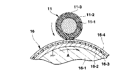
As shown in FIG. lB, the contact charging roller
11 of each of the four image forming units PU of the
electrophotographic color printer 31 shown in FIG. 6A
includes a round shaped metal bar 11-1 as a center
member, a roller-shaped conductive foam material
portion 11-2 covering the round bar, and a tube-shaped
conductive resin material portion 11-3 covering the
conductive foam material portion. And, as shown in
FIG. lA, a high voltage power supply 12 is connected to
the round bar 11-1. The round bar is formed of a
stainless steel and has a diameter of 6 mm. The
conductive foam material portion 11-2 is made of a
polyurethane foam which is formed by a reaction of
polyol with isocyanate and includes carbon particles as
conductive particles to make the foam material portion
have an electrical resistance of 103 Q. The conductive
resin material portion 11-3 is made of conductive nylon
tube which is formed by an extrusion molding to have
CA 0223~79~ 1998-04-24
a thickness of 100 ~ m and a surface resistance of
5 X 10⁶ Q/~.
The contact charging roller 11 as a whole has an
outer diameter of 10 mm, a hardness of Asker F 80~, and
5 an electrical resistance of 1 x 10⁶ Q.
FIG. 2 shows an apparatus for measuring the
surface resistance of the contact charging roller 11.
In this measuring apparatus, a load of 500g is applied
to each of both ends of the metal rod 11-1, the both
ends being projected in the longitudinal direction of
the roller 11 from the conductive foam and resin
material portions 11-2 and 11-3, so that the circular
surface of the roller is in contact with a measuring
electrode 13. And, a power source 14 output of which
is lOV is connected to the measuring electrode 13 and
the metal rod 11-1 through an ampere meter 15. At
this time, the ampere meter lS shows the resistance of
X 106 Q as that of the contact charging roller ll.
FIG. 3A schematically shows an interengagement
20 relationship between the contact charging roller 11 and
the photosensitive drum 16 in each of the four image
forming units PU of the electrophotographic color
printer 31 shown in FIG. 6A, and FIG. 3B schematically
shows a side view of the charging roller 11 and the
25 drum 16 shown in FIG. 3A.
As shown in FIGS. 3A and 3B, a drum supporting
shaft 17 of the photosensitive drum 16 is rotatably
CA 0223~79~ 1998-04-24
supported at its both ends by a pair of bearings 18a on
the unit frame 18 (see FIG. 6B) of the image forming
unit PU. A drum gear 19 is fixed to the drum
supporting shaft 17 at one end of the photosensitive
drum 16 and is selectably rotatably driven by a driving
system (not shown) of the printer 31. Both ends 21 of
the contact charging roller 11 are also rotatably
supported by a pair of bearings 22 on the unit frame 18
(see FIG. 6B) of the image forming unit PU, and a
pinion 23 fixed to one of the both ends 21 of the
contact charging roller 11 is in mesh with the drum
gear 19 so that the charging roller 11 is rotatably
driven by the rotation of the drum gear 19.
Alternatively, as shown in FIG. 3C, the contact
charging roller 11 may be rotatably driven by the
rotation of the drum gear 19 through a friction
produced between the surface of the roller 11 and the
circular surface of the drum 16. In this modification,
one of the both ends 21 of the contact charging roller
11 does not have the pinion 23 which is employed in the
above described one embodiment, and the above described
one of the both ends 21 of the contact charging roller
11 is only rotatably supported by a bearing 20 provided
on the frame 18. A structure for a contact relation-
ship between the contact charging roller 11 and thephotosensitive drum 16 in the modification shown in
FIG. 3C is simpler than that for an interengagement
CA 0223~79~ l998-04-24
-- 27
relationship therebetween in the above described one
embodiment shown in FIGS. 3A and 3B.
In each of the four image forming units PU of the
printer 31 of the present embodiment, the contact
charging roller 11 is pressed against the circular
surface of the drum 16 so that the charging roller
11 bites its surface into the circular surface of the
drum 16 by 0.4 mm. And the high voltage power source
12 applies a charging voltage which is produced by
superposing a direct current voltage VDc (about -700V)
on an alternating voltage VAc (a frequency of which is
about 1300 Hz) having peak-to-peak voltage Vpp of about
1400V to about 1500V to the metal center rod 11-1, so
that a charged potential of the circular surface of the
drum 16 is set at about -650V.
After the circular surface of the drum 16 is
charged uniformly as described above by the contact
charging roller 11, the inventors of the present
invention try to form an image, for example halftone
dots which is uniform in its whole area, on the
recording paper, and a very fine quality of halftone
dots image can be obtained. That is, there is no fault
in the image on the recording paper. More specifically,
not only a white belt or line will not formed on a
center portion of the image, the center portion
corresponding to the longitudinal center portion of the
circular surface of the photosensitive drum 16 from
CA 0223~79~ 1998-04-24
- 28
which the longitudinal center portion of the contact
charging roller 11 is left by the bent of the charging
roller, but also a lot of white spots will not formed
on a whole of the image, the white spots caused by an
insufficient contact of the charging roller 11 to the
circular surface of the photosensitive drum 16.
In this embodiment, the photosensitive drum 16
includes a conductive drum base 16-1 formed of an
aluminum, an anodized aluminum layer 16-2 formed on the
conductive drum base 16-1 to have a thickness of 5 ~ m,
an under coat layer 16-3 of synthetic resin formed on
the anodized aluminum layer 16-2 to have a thickness of
2 ~m, and a photosensitive layer 16-4 formed on the
under coat resin layer 16-3. A whole resistance of the
anodized aluminum layer 16-2 and the under coat resin
layer 16-3 is so set high, for example in a range from
109 Q to 101~ Q, that it does not lower characteristics
(for example, a charging characteristic and a
photoconductivity when the drum is exposed by light) of
the photosensitive drum 16. The above described high
resistance prevents electric charges with high voltage
uniformly charged on the photosensitive layer 16-4 by
the contact charging roller 11 and transportation
charges with low voltage formed in the uniformly
charged electric charges by exposing at least a portion
of the uniformly charged electric charges with light,
from escaping from the photosensitive layer 16-4.
CA 0223~79~ 1998-04-24
Further, since the anodized aluminum layer 16-2 has a
very high hardness, even if the circular surface of the
photosensitive drum 16 is damaged, the anodized
aluminum layer 16-2 and the conductive drum base 16-1
will not be damaged.
In the followings, how the above described
arrangement and structure of the contact charging
roller 16 according to one embodiment of the present
invention are set will be described in details.
At first, another contact charging roller having
the same structure and size as those of the contact
charging roller 16 according to one embodiment of the
present invention, but being different from the
charging roller 16 in their hardness is prepared. More
specifically, the hardness of the another contact
charging roller as a whole is Asker C 45~ which is the
same as that of the aforementioned conventional contact
charging roller as a whole described in Japanese Patent
No. 2,632,899, and the hardness of the contact charging
roller 16 according to one embodiment of the present
invention is Asker F 80~ as described above. It is
noted that the Asker C is used for designating a
hardness of something which has a relatively high
hardness, the Asker F is used for designating a
hardness of something which has a relatively low
hardness, and the hardness of something which has a
relatively low hardness will not be measured by the
CA 0223S79~ 1998-04-24
- 30
Asker C. Next, the another contact charging roller is
installed in an image forming unit of a printer, a
structure of the image forming unit being the same as
that of the image forming unit PU shown in FIG. 6B and
according to one embodiment of the present invention,
and the printer having only one image forming unit
described above.
And, by using the printer, image forming
operations are conducted for many times with changing
an amount of bite of the another contact charging
roller into the circular surface of the photosensitive
drum. FIG. 4A shows printing qualities obtained by the
printer with changing the amount of bite. In order to
compare to this, FIG. 4A further shows printing
qualities obtained by a printer in which only one image
forming unit is used and this image forming unit is the
same as the image forming unit PU shown in FIG. 6B and
using the contact charging roller 11 according to one
embodiment of the present invention.
In FIG. 4A, the printer using the contact charging
roller 11 (Asker F-80 ) can get good printing qualities
in cases that the amount of bite is set at 0.2 mm,
0.4 mm, and 0.7 mm, but not at 0 mm because many white
spots are formed in the image due to an insufficient
contact of the contact charging roller 11 against the
circular surface of the drum 16. In contrast to this,
the printer using the another contact charging roller
CA 0223~79~ 1998-04-24
(Asker C-45~) can not get good printing qualities in all
cases that the amount of bite is set at 0 mm, 0.2 mm,
0.4 mm, and 0.7 mm because many white spots are formed
in the image due to the insufficient contact of the
whole of the another contact charging roller against
the circular surface of the drum 16 in the cases that
the amount of bite is set at 0.1 mm and 0.2 mm, and a
white belt or line is formed in the image due to the
insufficient contact of the longitudinal center portion
of the another contact charging roller against the
circular surface of the drum 16 caused by bending of
the another contact charging roller.
In order to make the contact charging roller 11
have a good charging characteristic, that is to make
the printer using that contact charging roller 11 have
a good printing quality, both of the resistance of the
conductive resin material portion 11-3 and that of the
conductive foam material portion 11-2 must be set in
suitable ranges, respectively. And this range is
determined by an experiment performed by the inventors
of the present invention. FIG. 4B shows a result of
the experiment, and more specifically shows a
relationship between the charging characteristic of the
contact charging roller 11, that is the printing
quality of the image formed on the recording paper by
the printer, a change of the surface resistance of the
tube-like conductive resin material portion 11-3, and a
CA 0223~79~ l998-04-24
- 32
change of the resistance of the conductive foam
material portion 11-2.
As shown in FIG. 4B, a good charging charac-
teristic of the contact charging roller 11, that is the
good printing quality of the image formed on the
recording paper by the printer, is obtained when the
surface resistance of the conductive resin material
portion 11-3 is in a range from 1 x 10⁵ Q/O or more to
g x 107 Q/O or less and the resistance of the
conductive foam material portion 11-2 iS in a range of
9 x 10⁵ Q/O or less, preferably 9 x 10⁴ Q/O or less.
And, the conductive resin material portion 11-3 having
the surface resistance of the 104 Q/O or less can not
be realized because it must contain too much carbon
particles to form the resilient conductive resin
material portion 11-3.
FIG. 5 shows a method by which the tubular-shaped
conductive resin material portion 11-3 is fixed to the
conductive foam material portion 11-2 not to influence
the good charging characteristic of the contact
charging roller ll. According to this method, both
longitudinal ends of the tubular-shaped conductive
resin material portion 11-3 are fixed to both
longitudinal ends C of the circular surface of the
conductive foam material portion 11-2 by an adhesive,
and the both longitudinal ends C of the circular
surface of the conductive foam material portion 11-2
CA 0223~79~ 1998-04-24
are arranged in both outsides of a center portion B of
the circular surface which corresponds to an image
formation area on the circular surface of the
photosensitive drum 16 (shown in FIG. lB). That is,
the both longitudinal ends C correspond to both
longitudinal ends of the circular surface of the foam
material portion 11-2 and further correspond to image-
free areas arranged in both outsides of the image
formation area on the circular surface of the drum 16.
And, by preparing the tube-like conductive resin
material portion 11-3 independent of the conductive
foam material portion 11-2 on the center rod 11-1 and
by fixing the tube-like conductive resin material
portion to the circular surface of the conductive foam
material portion 11-2 with the adhesive, even if the
contact charging roller 11 having the two layers, that
is the conductive foam material portion 11-2 and the
conductive resin material portion 11-3, the contact
charging roller 11 can be formed easily and cheaply.
As describe above in detail, in the present
invention, since the hardness of the contact charging
roller as a whole is set at Asker F 90~ or less, the
contact charging roller can be in contact with the
circular surface of the image carrier uniformly even if
the roller is formed to have a smaller diameter than
that of the conventional one, so that the contact
charging roller of the present invention can charge the
CA 0223~79~ 1998-04-24
-- 34
circular surface of the image carrier uniformly to make
the image carrier have the good image, and the image
forming unit using the contact charging roller and the
electrophotographic image forming apparatus can be
S formed to have a small outer size.
And, since the image carrier of the image forming
unit of the present invention has the anodized aluminum
layer as a blocking layer and the photosensitive layer
provided on the anodized aluminum layer, further since
the image carrier of the one embodiment of the present
invention has an undercoat resin layer as an additional
blocking layer provided on the anodized aluminum layer
but under the photosensitive layer, withstand voltage
of the image carrier is increased and a leak of charges
from the image carrier is prevented, so that a
durability of the image carrier is increased with
maintaining the good image forming performance thereof.
More further, in the present invention, since the
tubular-shaped conductive resin material portion has
both end areas corresponding to the image-free areas of
the image carrier outsides of its image-forming area
and is fixed at the both end areas to the roller-shaped
conductive foam material portion by an adhesive, a
preparation of the conductive charge roller is easy and
will not influence the image forming quality formed on
the image carrier.
Additional advantages and modifications will
CA 0223~79~ 1998-04-24
-- 35
readily occur to those skilled in the art. Therefore,
the invention in its broader aspects is not limited to
the specific details and representative embodiments
shown and described herein. Accordingly, various
5 modifications may be made without departing from the
spirit or scope of the general inventive concept as
defined by the appended claims and their equivalents.