Note : Les descriptions sont présentées dans la langue officielle dans laquelle elles ont été soumises.
CA 0223~896 1998-04-27
Title: FIBER OPTIC GYRO WITH OPTICAL INTENSITY
SPIKE SUPPRESSION
BACKGROUND OF THE INVENTION
Field of the Invention
The invention relates to rotation rate sensors.
More particularly, the invention pertains to a method and
apparatus for reducing the influence of modulation
transition-induced voltage spikes upon the ouL~u~ of an
. interferometric fiber optic gyro.
Description of the Prior Art
In the operation of an interferometric fiber
optic gyro (IFOG) an artificial phase difference is
routinely superimposed between two counterpropagating
light waves by means of a phase modulator. The phase
modulation generally alternates in amplitude between +~/2
radians and the gyro output is sampled at those points,
which correspond to the points of maximum measurement
sensitivity of the interferometer output to rotation-
induced Sagnac phase shifts. Alternative modulation
schemes (so-called "overmodulation"), which employ phase
modulation depths that may exceed ~/2, are sometimes
CA 0223~896 1998-04-27
employed that offer other advantages such as improvement
in the signal-to-noise ratio.
A square wave modulation waveform in commonly
employed for generating the gyro output signal. While
such a waveform is readily approximated by the output of
present-day phase modulators, the transition between the
+~/2 modulation values is not instantaneous. Rather the
so-called square wave output of the phase modulator
includes discrete transition periods on the order of 100
nanoseconds during which the modulation assumes a
continuum of values between +~/2 and -~/2. This
phenomenon is illustrated in Figure 1, a graphical
representation of the square wave output of a gyro phase
modulator. As can be seen, while the modulation output
essentially shifts between +~/2 and -~/2, over small
periods of time ~t the phase modulator imposes all
artificial phase differences therebetween. As a
consequence, a large portion of the interferometer output
intensity range is scanned between these values.
Significantly, such range of values includes maximum
intensity as well as an infinite number of adjacent
values. It is well known that, at zero phase difference,
the energies of the two beams counterpropagating within
the gyro senscr coil produce total constructive
interference, resulting in maxima of the interferometer
CA 0223~896 1998-04-27
output characteristic (1 + cos~) where ~ is the phase
difference between the counterpropagating beams. This
same phenomenon occurs at ~ = n2~ where n is a (positive
or negative) integer.
Figure 2 is a graph of the above-described
relationship between interferometer output and phase
difference ~. The portion of the intensity-versus-phase
difference indicated in bold at 10 illustrates the
variation in interferometer output intensity that is
"picked up" as the square wave output of the gyro phase
modulator momentarily (i.e. over ~t) scans interferometer
output in shifting between the points of primary interest,
+~/2 and -~/2. The periodic compression of the output
scanning process into the periods of very small duration
~t is reflected in the measured gyro output by the so-
called "ears" 12 that are found in the intensity-versus-
time gyro output characteristic curve as illustrated in
Figure 3. Such ears are periodic and separated in time
from one another by r, the gyro sensor loop transit time.
In general, each transition spike in the output intensity
results from passage through the maximum point of the
intensity transfer function where the phase shifts from
one side to the other side of the maximum intensity value.
CA 0223~896 1998-04-27
The periods of the ouL~uL curve of Figure 3
between the ears, or output spikes, represent the useful
output intensities Ii and are determined in part by the
rate of rotation of the IFOG around the coil input axis.
Under the well-know Sagnac principle, the output of the
gyro experiences a phase shift ~ in the presence of a rate
of rotation about the sensor coil input axis. (Note, even
in the absence of rotation rate, ears are present in the
output of Figure 3 resulting from the modulation process
itself.) Commonly employed signal processing schemes for
extracting rotation rate information from detected signal
are based upon synchronous demodulation in which the
difference between successive signal levels Ii that
correspond to +~/2 modulation intervals is proportional to
the measured input rate.
No useful information is obtained during the
finite duration of a transition spike in the intensity
output (i.e. Figure 3) of a interferometric gyro. The
unavoidable presence of intensity spikes in the output of
present day IFOG's produces numerous problems. These are
generally related to the electronic operation and
performance of the gyro. Typically, present-day IFOG's
employ a photodetector to detect the optical output and to
generate a corresponding useful electrical signal. The
spikes in the optical intensity output produce pulses in
CA 0223S896 1998-04-27
the output of the photodetector. Such pulses can decrease
gyro accuracy despite the fact that the useful signal
between the transition spikes is only sampled after pulse
decay. The existence of pulse decay instabilities can
adversely affect high accuracy applications as
differential rates of decay may introduce rate measurement
errors. In addition, the relative amplitude of the
transition spike -as opposed to the useful signal- limits
the permissible gain of the gyro's front end signal
processing electronics as well as the maximum values of
front end amplifier feedback resistors. Such limitations
increase overall instrument noise, an effect that is
particularly evident in the case of very deep values of
overmodulation (~ ~ 3~/4). Alternatively, front end
saturation can cause significant performance problems as
the finite recovery times of the detector and/or front end
amplifiers require that the maximum possible values of the
feedback resistors of front end gain elements be limited
by the amplitudes of the spikes rather than those of the
useful signal.
Attempts to minimize the deleterious effects of
signal spikes have centered upon processing of the
resultant electrical output of the gyro and have included
the incorporation of a gate into the signal processing to
block photodetector output for the period corresponding to
CA 0223~896 1998-04-27
the intensity spike. Such solution is of limited benefit
with respect to gyro front end gain. Since the optical
intensity signal is received at the photodetector, the
problem of saturation of the photodetector and/or front
end amplifiers remains. Further, the incorporation of a
gate fails to address the errors that result from
differing rates of electrical pulse decay.
SUMMARY OF THE lNv~NllON
The present invention addresses the shortcomings
of the prior art by providing, in a first aspect, a fiber
optic rotation rate sensor. Such sensor includes a source
of optical energy. An optical fiber is formed into a coil
located intermediate its opposed ends. ~nc are provided
for dividing the output of the source into two light beams
and for launching the light beams into the fiber to
counterpropagate within the coil. ~e~nC are also provided
for imposing a periodic artificial phase difference
between the counterpropagating beams of light and for
recombining the counterpropagating beams into an optical
output signal.
Means are provided for selectively attenuating
the optical output signal. A photodetector receives the
selectively attenuated optical signal and converts it to a
responsive electrical signal.
CA 0223~896 1998-04-27
In a second aspect, the invention provides an
improvement in a rotation rate sensor of the type that
includes an optical fiber having an internal coiled
portion defining an input axis, a coupler for dividing
light traveling within the fiber upon entering the coil
into counterpropagating beams, a phase modulator for
applying a periodic, artificial phase difference between
the counterpropagating beams and a photodetector for
receiving an optical signal and converting it to an
electrical signal. The improvement provided by the
invention includes means for receiving the optical output
signal and producing a transformed optical signal for
application to the photodetector. Such means comprises an
electrooptical device.
In a third aspect, the present invention
provides a method for detecting rotation rate about a
predetermined space axis. Such method is begun by forming
a coil having an axis of symmetry interior of an optical
fiber. Such axis is then aligned with the predetermined
space axis. The output of a source of optical energy is
split to form two light beams and such light beams are
injected into opposite ends of the optical fiber whereby
the beams counterpropagate and interfere within the coil.
CA 0223~896 1998-04-27
Predetermined phase differences are periodically
imposed between the counterpropagating he;:l~C to modulate
them. The modulated optical output of the interfering
beams is received and selectively attenuated. The
attenuated optical output is converted into a
corresponding electrical signal which is then analyzed to
determine rotation rate.
The present invention addresses the problems
involved with phase modulation transition spikes by
attenuating the optical signal in the IFOG during
transition intervals. Each transition interval includes
the time at which the output intensity reaches a maximum
in the absence of the present invention. Attenuation of
the intensity of the optical signal reduces the maximum
signal reaching the detector during the phase modulation
transition period.
Numerous embodiments are provided in accordance
with the invention. One method includes attenuating the
intensity of the optical signal during transition
intervals below that of the useful signal. This way, the
values of front end gain f~h~ck resistors are limited by
useful signal, rather than the transition spike,
CA 0223~896 1998-04-27
amplitude. Of course, any degree of attenuation of the
transition spikes is beneficial.
An embodiment of this invention provides
apparatus for attenuating the optical signal in an IFOG
during transition intervals. An example of such an
apparatus is an intensity modulator between the fiber
coupler and the photodetector~
The present invention effectively decreases the
~Y;~um intensity of the optical signal that reaches the
detector during the transition intervals. Any decrease in
the maximum intensity results in the corresponding
reduction of limitations on the front end gain
characteristics of a typical detector. A decrease in the
maximum amplitude of the optical signal generated leads
also to a decrease in the amplitude of the tail of the
electrical signal. In fact, any degree of attenuation of
optical signal intensity spiking is beneficial.
An embodiment of the present invention provides
an electrical gate in combination with an optical
intensity modulator. The electrical gate blocks the
electrical output signal as residual transition interval
spiking of the optical signal is detected.
CA 0223~896 1998-04-27
A further embodiment contemplates the use of an
intensity modulator as an optical switch. Optical signal
attenuation is such that the intensity modulator prevents
almost all light from reaching the photodetector during
the transition intervals. The intensity of the light that
reaches the photodetector is dependent upon intensity
modulator quality. Examples of appropriate intensity
modulators include Mach-zeh~Aer interferometers and cutoff
modulators. Since nearly no light is incident upon the
photodetector during transition intervals, the front end
gain of the gyro signal processing electronics can be
determined from the intensity of the useful signal, rather
than that of the intensity spikes.
Various methods and devices may be employed to
modulate the intensity of the optical signal. In one
embodiment, a discrete cutoff modulator is located between
a coupler and the photodetector of the IFOG. Cutoff
modulators of 10-20 dB isolation result in received
intensity at the photodetector during transition times
being less than the useful outputs.
Other objects, features and advantages of the
present invention will become apparent from the detailed
description that follows. Such description is accompanied
by a set of drawing figures. Numerals of the drawing
CA 0223~896 1998-04-27
figures, corresponding to those of the written
description, point to the various features of the
invention. Like numerals refer to like features
throughout both the written description and the drawing
figures.
BRIEF DESCRIPTION OF THE DRAWINGS
Figure 1 i5 a diagram for illustrating +~r/2
square wave modulation for application to light beams
counterpropagating within the sensor coil of a fiber optic
gyro with transition times ~t exaggerated in duration;
Figure 2 is a diagram of the intensity-versus-
phase shift output characteristic of an interferometer
such as that exhibited by the output of the sensor coil of
a fiber optic gyro;
Figure 3 is a diagram of the intensity-versus-
time output characteristic of a fiber optic gyro for
modulation depths greater than zero and less than
radians illustrating the presence of the periodic
intensity spikes addressed by the present invention;
Figure 4 is a schematic diagram of an IFOG in
accordance with the invention;
CA 0223~896 1998-04-27
Figures 5(a) through 5(d) are a series of
waveforms for illustrating the operation of an IFOG in
accordance with the invention; and
Figures 6(a) and 6(b) are schematic diagrams of
alternative embodiments of IFOG's in accordance with the
invention.
DESCRIPTION OF THE PR~ KKED EMBODIMENT
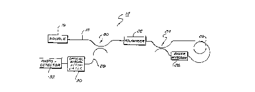
Turning to the drawings, Figure 4 is a schematic
diagram of an IFOG 14 in accordance with the present
invention. A source 16 of optical energy that may
comprise, for example, a superluminescent diode (SLD), a
laser diode, a superfluor~c~ent source, a light emitting
diode (LED) or equivalent means known to those skilled in
the art emits optical energy of predetermined wavelength
and bandwidth that travels through an optical fiber 18 to
a first coupler 20 and then to a polarizer 22. A second
coupler 24 receives the ouL~ of the polarizer 22,
dividing it into a pair of waves that counterpropagate
within a coil 26 of optical fiber whose central axis of
symmetry coincides with the sensitive or input axis of the
gyro 14.
A phase modulator 28 lies within the optical
path between the second coupler 24 and the optical fiber
CA 0223~896 1998-04-27
sensor coil 26 for applying a periodic artificial phase
difference between light waves counterpropagating within
the coil 26. Typically, the phase modulator 28 is
arranged to apply a square wave function such as that
illustrated in Figure 1. Upon exiting the coil 26, the
modulated, counterpropagating waves are combined to
interfere at the second coupler 24. The resultant optical
intensity signal is of the well-known form 1 + cos~ where
~ is the phase difference between the interfering light
waves. This optical intensity signal propagates bac~
through the polarizer 22 and to the first coupler 20 where
a portion of the intensity is coupled to a fiber 29 that
directs it to an optical signal attenuator 30. (The
representation of the attenuator 30 in the context of the
IFOG 14 of Figure 4 is generic and intended to support the
discussion of its basic operation. Specific alternative
embodiments of an IFOG in accordance with the invention
incorporating specific and distinct optical signal
attenuators are illustrated in Figures 6(a) and 6(b).)
The (optical signal) output of the attenuator 30 is
directed to a photodetector 32 for conversion to an
electrical signal suitable for electronic signal
processing, including electronic gating of any residual
modulation transition energy.
CA 0223~896 1998-04-27
The device 30 acts to ~uppress the deleterious
intensity spikes that characterize the interferometric
optical signal output of the second coupler 24. Figures
5(a) through 5(d) are a series of timing diagrams for
s illustrating the operation of an IFOG in accordance with
the invention. Figure 5(a), generally corresponding to
prior Figure 1 although of different scale, illustrates
the no~;n~l +~/2 square wave modulation applied by the
phase modulator 28. Figure 5(b), which replicates prior
Figure 3, illustrates the optical intensity-versus-time
output of the coupler 20, combining the counterpropagating
light beams from the sensor coil 26. The coupler 20 lies,
in part, in an optical path between the coil 26 and the
photodetector 32. As can be seen, the output signal of
Figure 5(b) is characterized by the inevitable presence of
ears or intensity spikes, separated in time by r, the
sensor coil loop transit time (as well as the period of
the applied optical phase modulation), whose origin is
described above. As discussed, the presence of such
intensity spikes in the interferometric optical output
signal has been addressed in the past by post-
photodetector 32 electronic signal processing techniques.
In the invention, by contrast, the device 30 acts upon the
optical signal prior to application to the photodetector
32, periodically attenuating the intensity of the optical
signal of Figure 5(b) to remove the intensity spikes prior
CA 0223~896 1998-04-27
to "conversion" of the information from the optical to the
electrical domain. By thus pre-filtering the harmful and
useless portions from the optical signal, the numerous
harmful effects that otherwise unavoidably impact upon~the
electronics of the gyro are avoided. Since significant
optical intensity spikes do not become inputs to the
photodetector 32, prior art gyro design limitations
related to handling of the resultant electrical signal are
mitigated. In the case of some applications, such as
those dealing with small amplitude optical signals, it
will still be advisable to process the electrical signal
output from the photodetector 32 by means of electronic
gates. However, in contrast with the types of electrical
gating apparatus necessitated by prior art arrangements,
much smaller and simpler electronic gates are required for
use in conjunction with the invention. As a consequence,
the saturation issues posed by electronic signal gating in
the prior art are much less significant in conjunction
with the invention.
Alternative arrangements and embodiments of the
invention will be discussed below. However, regardless of
the particulars of the embodiment chosen, the resultant
functioning of the invention may be described with
reference to the timing diagrams of Figures 5(a) through
CA 0223~896 1998-04-27
(d). Figure 5(c) is a timing diagram of the electrical
signal for driving the optical signal trimming device 30
of the IFOG 14. As is seen, the signal is periodic with a
period of r, the loop transit time. While the signal of
Figure 5(c) is illustrated as a single and pulsed signal,
its particular form will vary in accordance with the
physical arrangement of the device 30 within an IFOG in
accordance with the invention. The particulars of the
electrical signal for driving the device 30, in relation
to the type of modulator 30 employed, will be well
understood by those skilled in the art.
Returning to the timing diagram, Figure 5(d)
presents the optical output of the device 30. This
waveform, in contrast to the output of the coupler 24 (the
optical signal input to the device 30), is devoid of the
intensity spikes that characterize the optical waveform of
Figure 5(b). Rather, the intensity of the waveform of
Figure 5(d) in the regions of the former intensity spikes
may, in fact, be less than the useful signal portions
intermediate the end points of the loop transit modulation
periods. Such periodic diminutions of optical intensity
may be achieved in a number of ways in accordance with the
type of device 30 employed and its associated principle of
operation. Generally, however, it will be understood that
the optical signal trimming device 30, whatever its
16
CA 0223~896 1998-04-27
configuration, is electrooptic in nature, acting upon, and
causing resultant optical effects in response to a driving
electrical input. An electrooptical material, such as
LiNio3, provides an essential operative element of such a
device.
Figures 6(a) and 6(b) are schematic diagrams of
alternative embodiments of the invention characterized by
different physical arrangements for achieving the required
functional operation of the optical signal attenuator 30.
As far as other elements of the IFOG are arranged and
located, as in the "basic" configuration of Figure 4
above, such corresponding elements are referred to by like
numerals.
The embodiment of Figure 6(a) employs a so-
called cutoff or amplitude modulator as the optical signal
attenuator 30. As in the basic configuration, the cutoff
modulator is located in the optical path between the first
coupler 20 and the photodetector 32. Such location
assures that an optical signal of the form of Figure 3 (or
Figure 5(b)), with undesired intensity spikes, is received
at the attenuator 30. The modulator includes a substrate
34 of electro-optically active material such as LiNio3.
An elongated internal waveguide 36 is formed of highly-
doped LiNio3. Metallized electrodes 38 and 40 are located
CA 0223~896 1998-04-27
atop the substrate 34 at opposite sides of the waveguide
36. Such electrodes 38, 40 receive and apply
predetermined voltage signals across the waveguide 36,
producing electrical fields that control its optical
properties (i.e. mode field size). Referring back to
Figure 5(c), the application of such a periodic voltage
profile will render the waveguide 36 lossy on a periodic
basis. By altering the mode field size of the highly-
doped waveguide 36, light travelling through it becomes
correspondingly less guided, or unguided, propagating into
the substrate 34 rather than passing to the photodetector
32. In effect, the amplitude or cutoff modulator acts as
an optical choke in the presence of an appropriate
electrical signal. The periodic diminutions seen when one
compares the signals of Figures 5(b) and 5(d) to one
another reflect such operation of a cutoff modulator as
the attenuator 30.
The IFOG of Figure 6(b) employs a Mach-Zehnder
interferometer as the optical signal trimming device 30.
Again, such interferometer is located between the first
coupler 20 and the photodetector 32. The interferometer
is formed upon a substrate 42 of electro-optically active
material such as LiNio3. An upper waveguide 44 and a
lower waveguide 46 are formed of highly doped regions of
2S the substrate 42. The waveguides 44 and 46 meet at input
CA 0223~896 1998-04-27
. .
and output Y-junctions 48 and 50, respectively. The input
Y-junction 48 splits the input optical signal into two
signals that are "regrouped" at the output Y-junction 50.
Pairs of electrodes 52, 54 and 56, 58 are located at
opposite sides of the waveguides 44 and 46. The
interferometer operates by selectively retarding the phase
of light passing through one of the waveguides with
respect to that passing through the other. By controlling
the amount of phase retardation of light traveling through
one waveguide with respect to that traveling through the
other, one can control the destructive optical
interference that takes place at the output Y-junction 50.
In the event that, through the imposition of a voltage (or
voltages) of sufficient magnitude, a phase difference of
+~ radians were to be created between the light traveling
through the waveguides 44 and 46, total destructive
interference would take place upon recombination at the
output Y-junction 50, blanking the optical signal.
As can be seen, both an amplitude modulator and
a Mach-Zehnder interferometer may be effectively employed
as the optical signal trimming device of an IFOG in
accordance with the invention. In either case, a periodic
electrical driving signal of the form illustrated in
Figure 5(c) may be employed to reduce the optical signal
of Figure 5(b) that characterizes present day IFOG's to
CA 0223~896 1998-04-27
the form of Figure S(d). As discussed above, such an
optical signal, devoid of so-called ears, is much more
suitable for down-line electronic processing than that of
Figures 3 (or 5(b)). Further, the input of an optical
signal of the form of Figure 5(d) is readily processed and
significantly reduces design limitations upon gyro
electronics relative to large amplitude transition spikes.
While the benefits of the invention are apparent
when described with reference to the processing of the
optical output signal of a gyro modulated by the
imposition of conventional +~/2 phase modulation, the
apparatus and methods of the invention are equally
applicable to IFOG's that employ other periodic modulation
schemes. In fact, the benefits of the invention became
even more pronounced when applied to an IFOG employing
overmodulation (e.g. +3~/4). In such a case, the
intensity of the useful portion of the output optical
signal is less than that of +~/2 modulation. The r~
of the optical signal due to spiking are the same as in
the case of i~/2 modulation. Thus the absolute sizes of
the intensity spikes in the case of overmodulation are
greater from those for +~/2 modulation. For this reason,
the degradation of accuracy is greater in the case of
overmodulation and the benefits of the teachings of this
invention are correspondingly even greater.
CA 02235896 1998-04-27
The embodiments have been described in
considerable detail. However, it is to be understood that
the invention can be carried out by specifically different
methods and devices. Various modifications can be
accomplished without departing from the scope of the
invention itself.