Note : Les descriptions sont présentées dans la langue officielle dans laquelle elles ont été soumises.
CA 02236193 2000-06-22
- 1 -
SEMICONDUCTOR MICROWAVE AMPLIFIER
The present invention relates to a semiconductoY
microwave amplifier ba~;ed on a microstrip line mainly usino
a surface-mounted semiconductor amplification device for
which automatic mounting or reflow is easy to perform.
Conventiona7_ly, since a semiconductor microwave
amplifier of this type uses a small semiconductor amplifica-
tion device, the input and output electrodes of the semicon-
ductor amplification device are close to each other, so
high-frequency isolation can hardly be obtained. Conse-
quently, the deviation in frequency characteristics of the
gain increases, and additionally, little output power is
obtained, or the output power is positively fed back to the
input to easily cause oscillation.
Techniques for solving these problems have been
developed. In a microwave semiconductor device disclosed in
Japanese Examined Patent Publication No. 63-63121 (Japanese
Unexamined Patent Publication No. 57-141944), the semicon-
ductor amplification device is covered with a metal member
having an opening with a predetermined shape, thereby
obtaining desired isolation.
CA 02236193 1998-04-28
- 2 -
In a microwave amplifier disclosed in Japanese Unexam-
fined Utility Model Publication No. 1-122618, a sur-
face-mounted field effect transistor is used as the amplifi-
cation device to form a microstr_ip high-frequency amplifica-
tion circuit. In this microwave amplifier, the source
electrode is grounded using a through hole. However, since
the through hole has an indur_tance, the return loss de-
grades, the gain decreases, and oscillation or a decrease in
output power due to positive feedback occurs. To prevent
these disadvantages, the inductance of the through hole must
be lowered. For this purpose, a large-sized through hole is
used, and it is formed as close as possible to the source
electrode to decrease the excess distribution constant
between the source electrode a.nd the ground surface. This
measure also provides an effect for connection between the
ground electrode and the ground surface in use of a semicon-
ductor amplification device other than the field effect
transistor.
This measure is effective for the above-described
microwave semiconductor device disclosed in Japanese
Examined Patent Publication No. 63-63121 as far as the
semiconductor amplification device allows direct mounting on
the ground surface. However, in use of a semiconductor
amplification device to be surface-mounted on a printed-cir-
cuii~ board, when the semiconductor amplification device is
CA 02236193 2000-06-22
- 3 -
to be covered with a metal member, the structure becomes
complex because the printed circuit board must be subjected
to special working such as hole formation for metal member
attachment or connection for obtaining the ground surface.
Additionally, .in forming a microstrip amplification circuit,
the metal member must be connected to the ground electrode
at a low impedance. However, this process is diff icuit to
perform for the surface-mounted semiconductor amplification
device because of it:s shape.
In the microwave semiconductor device disclosed in
Japanese Examined Patent Publication No. 63-63121, the holes
formed in the printed-circuit board degrade isolation.
Therefore, if high-frequency isolation is required between
the upper and lower surfaces of the printed-circuit board,
and an internal layESr ground surface is formed, the ground
surface for the microstrip line is formed in the multilay-
eyed printed-circuit: board, so the above measure cannot be
applied.
Furthermore, in the microwave semiconductor device
disclosed in Japanese Examined Patent Publication
No. 63-63121, a general automatic mounting machine for
surface-mounted components performs only two-dimensional
component mounting and does not cope with such
three-dimensional assembly. For this reason, sur-
face-mounted c~emponents can hardly be automatically mounted.
CA 02236193 2000-06-22
- 4 -
In the microwave amplifier disclosed in Japanese
Unexamined Utility Model Publication No. 1-122618, a large
through hole must be formed near the ground electrode to
decrease the impedance. However, if device soldering is
performed using reflow, the solder flows into the through
hole. Solder necessary for fixing the ground electrode
may also flow into the through hole, resulting in degrada-
tion in soldering of the ground electrode. For this reason,
the connection impedance between the ground electrode of the
semiconductor amplification device and the ground surface
for the microstrip Line can hardly be lowered because of the
structure.
The present invention has been made in consideration of
the above situation of the prior art, and has as its object
to provide a semiconductor microwave amplifier which has a
low connection impcedance between the ground electrode and
the ground ;aurface of the semiconductor amplification
device, high isolation between the input and output and
between the Upper and lower surfaces of a printed-circuit
board in mounting on a multilayered printed-circuit board,
and a simple structure allowing use of an automatic mounting
machine.
In order to achieve the above object, according to the
first aspect of the present invention, there is provided a
CA 02236193 2000-06-22
- 5 -
semiconductor microwave amplifier comprising input- and
output-side microst rip lines formed on a printed-circuit
board to oppose each other, input and output electrodes
formed on the mic rostrip lines to be parallel to the
microstrip lines, a pair of ground electrodes formed in a
direction perpendicular to the input and output electrodes
to oppose each other, and a semiconductor amplification
device connected to all of the electrodes, comprising
electromagnetic connection shielding means, connected to the
ground electrodes, for ensuring high-frequency isolation
between the input electrode and the output electrode to
shield electromagnetic connection, and ground connection
means for connecting a ground portion of the semiconductor
device to a ground surface for the microstrip lines, the
ground surface being formed on the printed-circuit board.
According to the second aspect of the present inven-
tion, the ground connection means in the first aspect has a
through hole formation portion in the printed-circuit board.
According to the third aspect of the present invention,
the electromagnetic connection shielding means in the first
aspect has a portion inserted into a through hole formed at
the through hole formation portion of the printed-circuit
board and Nerving as solder flow prevention means for
preventing solder from flowing into the through hole.
According to the fourth aspect of the present inven-
CA 02236193 1998-04-28
- 6
tion, the electromagnetic connection shielding means in the
first: aspect has a flat portion serving as target chuck
means in mounting using an automatic mounting machine.
According to the fifth aspect of the present invention,
the <~lectromagnetic connection shielding means in the first
aspect is arranged on a side of the output electrode.
According to the sixth aspect of the present invention,
the electromagnetic connection shielding means in the first
aspect is arranged on a side of the input electrode.
According to the seventh aspect of the present inven-
tion, the printed-circuit board in the first aspect has a
multilayered structm_-e and has an internal layer set surface
for the input- and output-side microstrip lines.
As is apparent .from the above aspects, the semiconduc-
for microwave amplifier of the present invention has a metal
plate as the electromagnetic connection shielding means for
shielding electromagnetic connection between the input and
output electrodes of the semiconductor amplification device,
and a through hole as the connection means for connecting
the ground electrode of the semiconductor amplification
device to the ground surface for the microstrip lines. The
sem:i.conductor microwave amplifier also has a portion serving
as the flow prevention means at which the metal plate is
inserted into the through hole to prevent the solder from
flowing into the through hole in reflow, and a portion
CA 02236193 1998-04-28
serving as the target chuck means to be chucked by the
automatic mounting machine in mounting using the automatic
mounting machine. For this reason, the connection impedance
between the ground electrode of the semiconductor amplifica-
tion device and the ground surface becomes low. In addi-
tion,, isolation can be highly ensured between the input and
the output or between the upper and lower surfaces of the
prini~ed-circuit board in mounting on a multilayered
printed-circuit board. Furthermore, since the structure is
simple, easy assembly is enabled using an automatic mounting
machine.
More specifically, in this semiconductor microwave
amplifier, the metal plate serving as the electromagnetic
connection shielding means connected to the ground electrode
is placed between the input: electrode and the output
electrode of the semiconductor amplification device to
shield electromagnetic connection. With this structure,
since the isolation between the input and the output can be
improved, the deviation i.n frequency characteristics of the
gain is reduced. Sufficient output power can be obtained,
and oscillation generated upon positively feeding back the
output power to the input: can also be prevented.
The through hole for connecting the ground electrode of
the semiconductor amplification device to the ground surface
for the microstrip :Lines is closed. With this structure,
CA 02236193 2000-06-22
_ g -
even when a large through hole is used, solder is
prevented from f7_owing into the through hole to cause a
soldering failure for the ground electrode of the semicon-
ductor amplification device. For this reason, the ground
electrode o:E a surface-mounted semiconductor amplification
device to be attached by reflow can be connected to the
ground surf<~ce for the microstrip lines at a low impedance.
Therefore, the degradation in return loss, the decrease in
gain, oscil:Lation due to positive feedback, or the decrease
in output p~~wer can be prevented.
In addition, since all components can be mounted from
the upper surface side of the printed-circuit board, the
semiconductor microwave amplifier can be easily assembled
using a general automatic mounting machine allowing
two-dimensional component mounting.
Furthermore,, when the ground surface for the microstrip
lines is foamed in a multilayered printed-circuit board, the
internal layer ground surface has an isolation effect
between the upper and lower surfaces of the printed-circuit
board, so isolation between the upper and lower surfaces of
the multilayered printed-circuit board can be ensured. For
this reason, the component mounting density can be in-
creased.
The above and many other objects, features and advan-
tages of the pre:>ent invention will become manifest to those
CA 02236193 2000-06-22
_g_
skilled in the art upon making reference to the following
detailed description and accompanying drawings in which preferred
embodiments incorporating'the principles of the present invention
are shown by way of illust:rative example.
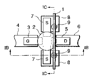
Figs. lA, 1B, and 1C are respectively: a plan view showing
the basic structure of a semiconductor microwave amplifier
according to the first embodiment of the present invention; a
sectional view taken alongi a line IB - IB in the plan view; and,
a sectional view taken along a line IC - IC in the plan view; and
Figs. 2A and 2E, are, respectively: a plan view showing the
basic structure of a semiconductor microwave amplifier according
to the second embodiment: of the present invention; and, a
sectional view taken along a line IIB - IIB in the plan view.
CA 02236193 2000-06-22
- 10 -
In the first embodiment of the semiconductor microwave
amplifier, ar.. inpu.t electrode 3 formed on an input-side
microstrip line 4 to be parallel to the microstrip line 4, an
output electrode 5 :Formed on an output-side microstrip line 6
to be parallel to the microstrip line 6 and opposing the input
electrode 3, and a pair of ground electrodes 7 formed on ground
lands 8 and Extending to oppose each other in a direction
perpendicular to the input and output electrodes are connected
to a semiconductor amplification device 2 on a printed-circuit
board 20. ThE~ semi~~onductor microwave amplifier also has a
metal plate 1 connected to the ground electrodes 7 and
serving as an electromagnetic connection shielding means for
ensuring high-frequency isolation between the input elec-
trode 3 and the output electrode 5 to shield the electromag-
netic connection, a:nd two through hole formation portions 9a
formed in th~~ printed-circuit board 20 and serving as a
ground connection means connected to a ground surface 10 for
the input-side microstrip line 4 and the output-side
microstrip line 6.
The metal plate 1 has a portion serving as a flow
prevention means wl:~ich is inserted into a through hol a 9b
formed at the' through hole formation portion 9a to prevent
a solder 11 from flowing into the through hole 9b in reflow.
CA 02236193 2000-06-22
- 11 -
More specifically, in this semiconductor microwave
amplifier, a microwave signal input from the input-side
microstrip li_:ne 4 passes through the input electrode 3 of
the semiconductor amplification device 2 and is amplified by
the semiconducaor amplification device 2, and then output to
the output-side microstrip line 6 through the output
electrode 5 of the semiconductor amplification device 2.
The ground electrodes 7 of the semiconductor amplification
device 2 are connected to the ground lands 8. The ground
lands 8 are connected to the ground surface 10 of the
output-side microstrip line 6 through the through hole
formation portions 9a. The metal plate 1 separates the
input electr~~de 3 from the output electrode 5 and is
partially inserted into the through hole 9b, so the metal
plate 1 is grounded and fixed by the solder 11. Before
reflow, the solder 11 is applied to the surfaces of the
ground lands 8. The ground electrodes 7 and the ground
lands 8 are simultaneously fixed upon reflowing the solder
11.
As the ~~ize o:E through hole 9b becomes larger, and the
number of through holes becomes larger, the impedance can be
lowered. The minimum inner diameter of the through hole 9b
should be 0.7 mm or more. The through hole 9b and the
ground electrode 7 are preferably close to each other. If
possible, the through hole 9b preferably contacts the ground
CA 02236193 1998-04-28
- 12 -
electrode 7 or is partially formed under the ground elec-
trode 7. In addition, the through hole 9b is preferably
formed close to the semiconductor amplification device 2.
ThesE~ conditions are necessary to lower the ground impedance
viewE~d from the semiconductor amplification device 2.
As the metal plate 1, a conductive material which can
be satisfactorily ~~oldered is preferably used. More
specifically, a solder-plated copper plate is suitable.
When the metal plate 1 is brought into contact with the side
wall of a metal container in which the semiconductor
amplification circuit is electromagnetically sealed, the
isolation effect can be further increased.
In the above-described first embodiment, the metal
plate 1 is arranged on the output electrode 5 side.
However, the metal plate 1 may be placed on the input
electrode 3 side.
Figs. 2A and 2B show the basic structure of a semicon-
ductor microwave amplifier according to the second embodi-
ment. of the present invention. Fig. 2A is a plan view, and
Fig. 2B is a sectional side view taken along a line IIB -
IIB in Fig. 2A.
In this semiconductor microwave amplifier, an inverted
U-shaped metal plate 12 formed by sheet metal working to
have a flat surface is used in place of the metal plate 1,
so chucking by the nozzle of an automatic mounting machine
CA 02236193 1998-04-28
- 13 -
is allowed, unlike the first embodiment. More specifically,
the inverted U-shaped metal plate 12 includes a portion
serving as a target chuck means in mounting using an
automatic mounting machine. For this reason, chucking by
the nozzle of the automatic mounting machine is allowed to
improve the attaching properties.
In this semiconductor microwave amplifier, an internal.
layer ground surface 13 for an input-side microstrip line 4
and an output-side microstrip line 6 is formed using an
internal surface of a multilayered (in this case, four-lay-
er) printed-circuit board 20, thereby ensuring high-fre-
quen~~y isolation from the lower surface of the printed-cir-
cuit board 20. Therefore, another circuit can be arranged
on t:he lower surface of the printed-circuit board 20, so the
number of components mounted per unit area can be increased.
In addition, this semiconductor microwave amplifier has
four through holes 9b. With this structure, the connection
impedance between a ground e:Lectrode 7 and the internal
layer ground surface 13 for the input-side microstrip line
4 and the output-side microstrip line 6 can be lowered.
Note that the portion of the inverted U-shaped metal
plate 12, which serves as a target chuck means in mounting
using the automatic mounting machine, may also be formed on
the metal plate 1 of the first embodiment.
As is apparent i=rom the above description, the semicon-
CA 02236193 1998-04-28
- 14 -
ductor microwave amplifier of the present invention is
characterized by comprising a metal plate serving as an
electromagnetic connection shielding means for shielding the
electromagnetic connection between the input electrode and
the output electrode of the semiconductor amplification
device, and a through hole formation portion serving as a
connection means for connecting the ground portion of the
semiconductor amplification device to the ground surface for
the microstrip line :Formed on the printed-circuit board at
a low impedance. The metal plate is connectea to zne grouna
electrode at a low impedance so as to shield an electromag-
netic wave directly coupled between the input and output
through the peripheral space of the semiconductor amplifica-
tion device. This metal plate has a portion inserted into
the through hole and serving as a flow prevention means for
preventing a solder from flowing into the through hole in
reflow, and a portion serving as a target chuck means to be
chucked by an automatic mounting machine in mounting using
the automatic mounting machine.