Note : Les descriptions sont présentées dans la langue officielle dans laquelle elles ont été soumises.
CA 02236202 1998-07-21
ELECTROCHEMICAL DISPLAY CELL WITH FOCUSED FIELD
This application claims the benefit of U.S. Provisional
Application No. 60/045,051, filed on 28 April 1997, which
provisional application is incorporated by reference herein.
5 TEC~INICAL FIELD
The invention relates to thin flexible displays incorporating.
electrochemical mechanisms for displaying visual information. The
displays are preferably self-powered, irreversible, low cost, and
formed in layers that can be printed on an in-line press.
10 BACKGROUND
Electrochemical reactions are among the mechanisms that have
been used for selectively displaying visual information ranging from
pure color to text or graphics. The visual information can be hidden
from sight and later revealed by the electrochemical reactions, or
15 the electrochemical reactions can be controlled to produce the
visual information.
For example, U.S. Patent 5,500,759 to Coleman discloses an
electrochemical display that can be activated to change color in a
predetermined pattern laid out by electrodes. Coleman's design
20 requires an external power source and special electrochromic
materials that can be quite expensive. U.S. Patent 4,804,275 to Kang
et al. discloses a self-powered electrochromic timing device in
which a color change boundary in an electrochromic material is
advanced by a gradual dissolution of an electrode. Kang et al.'s
25 electrochromic reactions require a strong acid and other materials
that add cost and pose problems for manufacture and use.
Electrode dissolution has also been used in electrochemical
display cells to reveal information otherwise obscured by an
electrode. For example, U.S. Patent 4,153,345 to Duchéne et al.
30 discloses an electrolytic display cell in which a pattern of thin
CA 02236202 1998-07-21
metal film is alternately dissolved into a liquid electrolyte and
redeposited onto conductive portions of a transparent electrode. An
insulator covers selected portions of the transparent electrode to
pattern the depositing metal film. The polarity of an external power
5 source controls whether the display undergoes dissolution or
deposition .
Duchéne et al. capture the electrolyte between two electrodes.
One of the electrodes is a transparent film such as In2O3 or SnO2; and
the other electrode, which undergoes dissolution and deposition, is
10 made from a material such as silver. Both electrode materials can
be quite expensive, and a separate power source is required to
operate the display. Manufacture is also complicated by locating a
liquid electrolyte between the two electrodes, requiring each to be
supported on a separate substrate.
U.S. Patent 5,339,024 to Kuo et al. discloses a charge indicator
cell connected in parallel with a main cell. An anode carried on a
conductive substrate of the indicator cell is gradually oxidized to
reveal a message written in ink on an underlying layer. One
embodiment arranges the electrolyte between the anode and a
20 cathode in the form of a stack. Another embodiment arranges the
anode and cathode side-by-side and fashions the electrolyte as a
porous film straddling both electrodes. Both embodiments are
subject to "islanding", where portions of the anode become
electronically isolated from the cathode in advance of the anode's
25 total disappearance. In the side-by-side arrangement, the path of
ion conduction becomes increasingly inefficient as the anode erodes
further from the cathode. Separate substrates are also used in both
embodiments for supporting the electrodes, which complicates
manufacture.
30 SUMMARY OF INVENTION
Our new display cells, which are preferably both self-powered
and irreversible, can be arranged in layers to achieve such further
objectives as facilitating in-line production, lowering production
costs, enhancing performance, simplifying use, and integrating the
CA 02236202 1998-07-21
display cells with other printed products such as labels. Two
electrode layers of our display cells can be arranged in the form of a
stack with one electrode layer only partially covering the other. An
electrolyte layer can be arranged to cover laterally separated
5 portions of the two electrode layers. This arrangement facilitates
printing of both electrode layers and the electrolyte layer on the
same substrate or web. An interface between the two electrodes
can be shaped to optimize performance.
One of the electrode layers is preferably a thin continuous film
10 deposited directly on the web. The other layers, which include the
other electrode layer, a dielectric layer separating the two
electrode layers, and the electrolyte layer, can be printed on the
film in repeating patterns one layer over the other to produce a
succession of electrochemical display cells. Aligned openings
15 formed through portions of the other electrode layer and the
dielectric layer expose portions of the thin-film electrode layer. A
common face of the electrolyte layer contacts both the remaining
portions of the other electrode layer and the exposed portions of the
thin-film electrode layer to complete an ionically conductive
20 pathway between the electrode layers. A flow of current (i.e.,
activation of the cell) causes the exposed portions of the thin-film
electrode to disappear in a controlled manner to reveal
predetermined visual information.
Unlike other disappearing electrode displays, the path of ion
25 conduction between electrode layers takes place through a pattemed
opening or aperture in one of the electrode layers. For example, the
thin-film electrode layer can function as an anode, and the other
electrode layer can function as a cathode. Openings through the
cathode layer and the dielectric layer are aligned for exposing a
30 portion of the anode layer. The electrolyte layer is applied over the
surface of the cathode layer including its opening through which the
electrolyte comes into contact with the exposed portion of the anode
layer.
Completing a separate electronically conductive pathway
3 5 between the anode and cathode layers triggers an electrochemical
CA 02236202 1998-07-21
reaction that produces a focused electric field within the
electrolyte layer. Current flow cascades from the surface of the
cathode layer through the aligned openings in the cathode and
dielectric layers to the exposed portion of the anode layer. The
5 spontaneous electrochemical reaction supported by the focused flow
of current erodes (i.e., oxidizes) the exposed portion of the anode
layer revealing visual information such as color, text, or graphics
prinled behind the anode layer.
Experimental moclels produced on a press indicate that for
10 limited size openings in the cathode and dielectric layers (e.g., one
centimeter or less), the electrochemical erosion of the exposed
portion of the anode layer is usually total. The openings are
preferably circles for revealing underlying colors or graphics but can
also take a variety of other geometric shapes or even fractal shapes
15 including characters or other graphic patterns. In addition, multiple
openings can be formed through the same cathode and dielectric
layers exposing additional portions of the same anode layer for
displaying more information such as a series of letters or
characters. The visual information revealed as a result of anode
20 erosion can be printed on substrate backings of the anode layer or
the cathode layer to allow viewing through the openings in the
cathode and dielectric layers.
The continuous thin-film anode layer is preferably a sputtered
or metalized aluminum deposited onto a transparent substrate such
25 as a polyester or other polymer-based film. Aluminum, along with
certain other metals and metal alloys, can be used as non-reversible
anodes. Carbon along with certain materials such as manganese
dioxide, silver, or other metals well separated in the
electrochemical scale from the anode material can be used as
30 cathodes. By suitable choice of the cathode and electrolyte
materials with respect to the anode material, the rate of anode
disappearance (i.e., clearing rate) can be controlled. Other
influences on the clearing rate include the sizes and shapes of the
openings in the cathode and dielectric layers, the size and shape of
35 the cathode layer, the conductivity of the electronically conductive
CA 02236202 1998-07-21
pathway between the anode and cathode layers, and the conductivity
within the anode and cathode layers themselves.
The electrolyte can be in the form of a liquid or gel or can be
mixed in with an adhesive such as an animal glue or a pressure-
5 sensitive, UV-curable variety. The electrolyte mix can also function
as a binder for the overall structure and as an additional spacer
between the anode and cathode layers.
In other embodiments, the ionically conductive pathway
between electrodes is interrupted to control or defer activation of
10 the display cell. For example, the electrolyte layer can be separated
from one or both electrodes until required for use. This can extend
shelf life, which could otherwise be shortened by unwanted erosion
of the anode by components of the electrolyte mix. Activation is
deferred by maintaining the electrolyte layer out of contact with one
15 of the electrode layers until it is time to place the display cell into
service. The electrolyte can be brought into contact with the
electrolyte layers by physically joining different parts of the
display cell or by rupturing a temporary barrier separating the
electrolyte layer from one of the electrode layers.
Our new display is particularly well suited for manufacture
along an in-line press. All of the active layers including the two
electrodes, the electrolyte, and the electronic connection between
the electrodes can be printed on a single web. Other printed layers
or webs can be combined to provide the visual information, sealing
for the electrolyte, or adaptations to other products such as
pressure-sensitive labels. Alternatively, the electrolyte layer can
be printed on a separate web and laminated to the two electrode
layers to complete a similar succession of display cells. The
completed display cells are particularly useful for such products as
game pieces, message cards, tamper-evident seals, time-elapsed
indicators, and other single-use indicators.
For purposes of this invention and its continuing description,
the terms "erode", "oxidize", "dissolve", "clear", and "disappear"
are used interchangeably as they pertain to the systematic removal
of thin-film electrodes.
CA 02236202 1998-07-21
DRAWINGS
FIG. 1 is a plan view of a circularly configured voltaic, self-
powered display cell arranged for revealing a visual image behind an
eroding film boundary through a circular aperture.
FIG. 2 is a cross-sectional view of the display cell taken along
line 2-2 in FIG. 1 showing the display cell mounted on a label
structu re .
FIGS. 3A-3F show progressive stages of assembly for the
display cell in an order that the various layers could be applied along
an in-line press.
FIG. 4 is a plan view of a similar self-powered display cell
having a rectangular shape and an alternative electrical switch.
FIG. 5 is a cross-sectional view of a switch arm for activating
the display cell of FIG. 4.
FIGS. 6A and 6B provide cross-sectional illustrations of a
display cell in both inactive and active states distinguished by the
state of ionic conduction between electrode layers.
FIG. 7 is a plan view of another display cell distinguished by
an ionically conductive pathway interrupted by a passivation layer.
FIG. 8 is a cross-sectional view taken along line 8-8 of FIG. 7.
FIG. 9 is a diagram of an in-line press for manufacturing the
display cells.
DETAILED DESCRIPTION
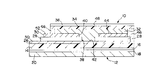
A self-powered (voltaic) display cell 10 depicted in FIGS. 1-3F
25 is mounted on a circular label 12 having a common substrate 14. The
label 12 includes a graphics layer 16, which can be printed on either
side of the common substrate 14, and a pressure-sensitive adhesive
layer 18, which is protected by a release liner 20. The common
substrate 14 is preferably a transparent film, such as Mylar
CA 02236202 1998-07-21
polyester or PET (polyethylene terephtalate). The graphics layer 16,
which can range from a patch of color to text or other graphic
patterns, provides a visible image for eventual display. The release
liner includes a layer of release, such as silicone, on another
5 substrate, such as kraft paper.
The display cell 10 has a thin metal film electrode (e.g., anode)
layer 26, whicll has been deposited (e.g., sputtered Ol otherwise
metalized) onto the common substrate 14. Aluminum is the
preferred metal of the thin metal film because of its low cost and
10 ready availability in thin-film form. A separate backing layer could
also be used to support the thin-film electrode layer 26 during its
manufacture and subsequent assembly with the substrate 14.
A dielectric layer (e.g., varnish) 28 and another electrode (e.g.,
cathode) layer 30 are printed in succession on the thin-film
1 5 electrode layer 26 in patterns that form concentric circular
apertures (openillgs) 38 and 40 through which a designated portion
42 of the electrode layer 26 remains exposed. The circular aperture
38 of the dielectric layer 28 is a little smaller than the circular
aperture 40 of the electrode layer 30 to assure that the two
20 electrode layers 26 and 30 remain electronically isolated within the
designated portion 42. The electrode layer 30 can be made of carbon
and function as its own current collector, or another electrode
material such as manganese dioxide could be printed over a carbon
collector. The electrode layer 30 could also be constructed as a thin
25 metal layer, such as silver, deposited onto a backing layer that could
augment or even replace the dielectric layer 28.
An electrolyte layer 32, which can also be applied by printing
or other means such as lamination, overlaps a surface 44 of the
electrode layer 30 and the designated portion 42 of the electrode
30 layer 26 for providing an ionically conductive pathway between the
electrode layers 26 and 30. A common face of the electrolyte layer
32 contacts both electrode layers 26 and 30. Another clear
substrate 34 made from a material such as PET covers the
electrolyte layer 32 and is bonded to the common substrate 14 with
35 a dielectric adhesive layer 46, such as hot-melt adhesive, that
CA 02236202 1998-07-21
forms a peripheral boundary of the electrolyte layer 32. Preferably,
the electrolyte layer 32 also has adhesive properties for further
attachil1g the clear substrate 34. An electrolytic adhesive can be
made by mixing an electrolytic salt into an adhesive, such as a
5 pressure-sensitive or UV-curable adhesive or an animal glue.
The substrate 34 is covered by a graphics layer 36 that
includes a window 48 aligned with the apertures 38 and 40 through
whicl1 the designated portion 42 of the electrode layer 26 is visible.
The graphics layer 36 preferably contains printed information
1 0 related to the eventual display of the graphics layer 16 in the
window 48.
FIGS. 3A-3F illustrate a step-by-step construction of the
display cell 10, which is particularly well suited for manufacture by
an in-line press. To the electrode layer 26 is applied the dielectric
15 layer 28 in a pattern that includes a circular aperture 38
surrounding the designated portion 42. The electrode layer 30 is
applied entirely within the dielectric layer 28 with its circular
aperture 40 aligned with the circular aperture 38 of the dielectric
layer 28. The dielectric adhesive layer 46 surrounds limited
20 peripheral portions of the dielectric layer 28 and the electrode layer
30 and provides a mask for confining the electrolyte layer 32 within
the cell. The clear substrate 34 covers all but a similar remaining
part of the cell periphery. The window 48 in the graphics layer 36 is
aligned with the concentric apertures 38 and 40 and the designated
25 portion 42. Along a remaining part of the cell periphery, exposed
portions 50 and 52 of the electrode layers 26 and 30 provide
electrical contacts for completing an electronically conductive
pathway between the electrode layers 26 and 30. An electronically
conductive layer (not shown), such as carbon, can be applied to the
30 exposed portion 50 of the thin-film electrode layer 26 to increase
its durability for electrical contact.
Folding the exposed portion 50 of the electrode layer 26 into
contact with the exposed portion 52 of the electrode layer 30
produces a path for current to flow through the display cell 10 and
35 triggers an electrochemical reaction that produces a focused
CA 02236202 1998-07-21
electric field within the electrolyte layer 32. Current flow
cascades from the surface 44 of the electrode layer 30 through the
concentric apertures 38 and 40 to the designated portion 42 of the
electrode layer 26. The spontaneous electrochemical reaction
5 supported by the focused flow of current erodes (i.e., oxidizes) the
designated portion 42 revealing the graphics layer 16, which can
contain visual information such as color, text, or graphics.
The display cell 10 is substantially depleted when the
designated portion 42 is cleared because no other portion of the
10 thin-film electrode layer 26 is initially exposed to the electrolyte
layer 32, except that the electrolyte layer 32 will then begin to
creep slowly between the dielectric layer 28 and the common
substrate 14 eroding adjacent portions of the electrode layer 26 at a
much slower rate.
1 5 Display cell 60 depicted in FIG. 4 is similar in many respects
to the display cell 10 of the preceding figures but has a rectangular
shape and an alternative electrical switch whose switch arm 70 is
depicted in FIG. 5. Similar to the preceding embodiment, exposed
portions 62 and 64 of two electrode layers separated by a dielectric
20 layer 66 function as electrical contacts. The switch 70 is sized to
complete an electronically conductive pathway between the exposed
electrode portions 62 and 64.
As shown in FIG. 5, the switch arm 70 is made by means of a
conductive tape 72 laminated onto a strip of thin metallic film 74,
25 such as copper or aluminum, and overlaid by a graphics layer 76
indicating how the user is to place the switch to activate the
display cell 60. A release liner 78 protects the conductive tape 72
until ready for use. An example of the conductive tape 72 is 3M
product number 9703. The referenced tape 72 is conductive normal
30 to its plane of lamination; and the metallic film 74, which is in
contact with the tape 72, carries current parallel through this plane
for bridging the gap between the electrode portions 62 and 64.
Activation of the display cell 60 is accomplished by removing
the release liner 78 and applying the switch arm 70 across the
35 exposed electrode portions 62 and 64. The conductive tape 72 forms
CA 02236202 1998-07-21
1 0
a permanent bond with the electrode portions 62 and 64 so that no
further action is required to maintain the display cell 60 in an
active state.
In place of a separate switch arm 70, a similar conductive tape
5 could be applied to just one of the electrode portions 62 and 64 and
covered with a release liner to protect the tape prior to use. After
peeling away the release layer, the electrode portions 62 and 64
could be permanently folded together trapping the conductive tape
between them. Such single-pole switching can also be accomplished
10 in a variety of other ways including as a consequence of other
actions that are related to the use of the display cell. For example,
the display cells could be used to provide tamper evidency by
activating when a bottle or other form of packaging is opened or
closed.
1 5 The ionically conductive pathway between the electrodes could
also be interrupted to provide a switching function in addition to or
as a replacement for one of the just-described electrical switches
that interrupt the electrically conductive pathway between the
electrodes. Interrupting the ionically conductive layer, such as by
20 isolating the electrolyte layer from one or both of the electrode
layers, can have the added advantage of extending shelf life of the
display cells by reducing the risk of self-activation.
FIGS. 6A and 6B depict inactive and active layouts of a display
cell 80, whose ionically conductive pathway is interrupted to
25 provide a switching function. In the inactive state as depicted by
FIG. 6A, two electrode layers 82 and 84 partially separated by a
dielectric layer 86 are mounted on one-half of a transparent
substrate 88, and an electrolyte layer 90 captured within a
surrounding dielectric adhesive layer 92 is mounted on the other half
30 of the transparent substrate 88. The electrode layer 82 is
preferably a thin film, such as aluminum, deposited onto a backing
102. Graphics (not shown) can be located on either side of the
transparent substrate 88 or the backing 102 to give meaning to the
display 80. A release layer 94 protects exposed surfaces of the
35 electrolyte and dielectric adhesive layers 90 and 92.
CA 02236202 1998-07-21
Concentric openings 96 and 98 are formed in the electrode
layer 84 and the dielectric layer 86 exposing a designated portion
100 of the electrode layer 82. The dielectric layer 86 separates
(i.e., electronically isolates) the electrode layers 82 and 84 in the
5 vicinity of their intended mutual contact with the electrolyte layer
90. However, a conductive adhesive layer 104 joins peripheral
portions of the two electrode layers 82 and 84 for completing an
electronically conductive pathway beyond any region of their
intended rnutual contact with the electrolyte layer 90.
As shown in FIG. 6B, the display cell 80 is activated by
removing the release liner 94 and folding the transparent substrate
88 together so that the electrolyte layer 90 overlaps the electrode
layer 84 and extends into contact with the designated portion 100 of
the electrode layer 82 for completing an ionically conductive
15 pathway between the electrode layers 82 and 84. Since the
conductive adhesive layer 104 permanently completes the
electronically conductive pathway between the two electrode layers
82 and 84, subsequent completion of the ionically conductive
pathway triggers electrochemical reaction resulting in the erosion
20 of the designated portion 100 of the electrode layer 82.
Both the electrolyte layer 90 and the dielectric adhesive layer
92 are formed as pressure-sensitive adhesives to provide better
bonding with the electrode layers 82 and 84. Upon applying pressure
to the folded layers of the transparent substrate 88, the pressure-
25 sensitive electrolyte layer 90 permanently completes a circuitbetween the electrode layers 82 and 84 so as to produce the
electrochemical reaction that erodes the designated portion 100 of
the electrode 82 and reveals the underlying graphics.
Another example of a display cell with an interrupted ionically
30 conductive pathway is illustrated by FIGS. 7 and 8. The illustrated
display cell 110 is similar to the assembled display cell 80 of FIG.
6B but has a passivation layer 112 separating an electrolyte layer
114 from a thin-film electrode layer 116. The passivation layer 112
comprises a fragile dielectric material that also electronically
35 separates the thin-film electrode layer 116 from an overlying
CA 02236202 1998-07-21
1 2
electrode layer 118 in the vicinity of their intended mutual contact
with the electrolyte layer 114. A conductive adhesive layer 122
joins peripheral portions of the electrode layers 116 and 118 to
complete an electrically conductive pathway between the electrode
5 layers 116 and 118.
A graphics layer 124 on a top substrate 126 includes a window
128 along with instructiol1s for activating the display cell 110, such
as by rubbing or scratching the window 128 or by folding the entire
display cell 110, to break the passivation layer 112. Once broken,
10 the passivation layer 112 permits the electrolyte layer 114 to seep
into contact with a designated portion 130 of the thin-film
electrode layer 116 thereby completing an ionically conductive
pathway between the electrode layers 116 and 118.
The resulting erosion of the designated portion 130 reveals an
15 underlying visual image formed by a graphics layer 132 printed on a
bottom substrate 134, which together with the top substrate 126
and a dielectric adhesive layer 136 provides the structural support
for the display cell 110. A pressure-sensitive label structure could
also be appended to the display cell 110 or to any of the preceding
20 display cells as shown in FIG. 2.
Also, instead of viewing an, image revealed behind the thin-
film electrode layer 116 through a window 128 in a top substrate
126, the display cell 110 (as an example of all the preceding display
cells) could be inverted and the graphics layers 124 and 132
25 rearranged to provide a similar viewing opportunity through a
window in the bottom substrate 134. In this alternative line-of-
sight direction through the display cell 110, the electrode layer 118
could be reshaped to help form the image that is revealed by erosion
of the electrode layer 116. The electrode layer 118 could also be
30 formed with multiple apertures for exposing additional portions of
the electrode layer 116 to reveal more than one visual image or a
more complex single image in either viewing direction.
The clearing rate of the designated portions of the thin-film
electrode layer can be controlled by suitable choices of the
35 electrode and electrolyte materials. The shapes and sizes of the
CA 02236202 1998-07-21
1 3
electrode layers, the volume of electrolyte, and the conductivity of
the electronically conductive pathway can all be arranged to further
influence the clearing rate. Normally, rapid clearing of the
designated portions of the thin-film electrode layer is desired to
5 provide a quick response to events that trigger activation of the
display cells. However, more gradual clearing of the designated
portions can be used to provide a timing function.
A diagram of an in-line press that can be used to print and
assemble the display cells described here is shown in FIG. 9. A
10 bottom substrate 150 is unrolled and advanced to a print station 152
for application of graphics. A metalized film 154, such as vapor-
deposited aluminum, is laminated at station 156 to the printed
bottom substrate 150. A dielectric layer is applied in a succession
of patterns to the metalized film 154 at station 158, followed by
1 5 the application of a patterned carbon electrode layer at station 160,
a patterned UV-curable adhesive at station 162, and a UV-curable
adhesive electrolyte at station 164. A top substrate 166 is unrolled
ancl laminated over the successions of patterns on the bottom
substrate 150 at station 168. A UV-curing station 170 cures the
20 adhesive layers to permanently bond the substrates 150 and 166
together. Another printing station 172 applies more graphics, and a
die cut station 174 divides the successively patterned portions into
individual display cells that can be stacked, rolled, or further
processed .
The thin metal films arranged as disappearing electrode layers
in the preceding embodiments are all preferably formed by
deposition onto non-conductive substrates and are distinguished
from metal foils that are thinned from thicker metal forms.
Deposition methods include vacuum evaporation, cathode sputtering,
electroplating, and various chemical reactions in a controlled
atmosphere or electrolyte. The deposited metal for the anode
electrode is preferably aluminum; but other metals could also be
used, such as copper, zinc, silver, or gold. The deposited material
for the cathode electrode is preferably carbon, but thin films such as
silver can also be used in combination with the aluminum film anode.
CA 02236202 1998-07-21
1 4
The display cells can be switched from a first state in which
the thin metal film of the anode is opaque to a second state in which
a designated area of the thin metal film becomes substantially
transparent, but the display cells cannot be restored to the first
5 state. The erosion that takes place in the thin metal films to reveal
visual images is irreversible. The visual images remain permanently
displayed through transparent portions of the non-conductive
substrates that support the thin metal films.
All of the substrates, including the substrate that normally
10 supports the thin metal film and the pressure-sensitive adhesive-
backed label stock are preferably supplied in rolls that can be
unwoulld into an in-line press. All of the other layers, including the
electrodes, the electrolyte, the dielectric, and the adhesives as well
as the visual image, are preferably printed in patterns on one of the
15 substrates by printillg stations that are arranged along the press.
Flexographic printing is preferred, but screen printing or other
extrusion techniques may be required for printing the adhesives.
The thin metal films are preferably predeposited onto the top
substrates in advance of any press operations. However, a thin
20 metal film could also be transfer printed from a temporary carrier
to the top substrate along the press, such as by hot or cold stamping.
For example, a thin metal film could be transferred from the
temporary carrier by cold stamping in a pattern that matches an
adhesive pattern on the new substrate for shaping the electrodes.
Sucl- in-line processing can be used to produce successions of
electrochemical display cells in large volumes at low cost.
Additional stations, such as die cutters, laminators, or applicators,
can be used to adapt the displays for their intended use as stand-
alone display cells or as display cells incorporated within other
products.