Note : Les descriptions sont présentées dans la langue officielle dans laquelle elles ont été soumises.
CA 0223684~ l998-0~-06
~,
<
Wo 97/17605 PCT/EP96/04853
Process and circuit arrangement for testing solder
joints
The invention relates to a process and a
circuit arrangement for testing solder joints according
to the precharacterizing clause of the independent
claims and, respectively, according to Clalm 21.
The quality of solder joints on printed circuit
boards can be checked for defects by means of X-rays.
In the process, solder-joint-specific quality
information is formed, either the information "solder
joint defect-free" or the information "solder joint
defective" being formed for each solder joint. This
information is printed out with reference to printed
circuit boards, this print-out, together with the
associated printed circuit board, being supplied to a
repair workstation. There, the printed circuit boards
which have at least one solder joint for which the
information "solder joint defective" was formed is
subjected to subsequent treatment, the allegedly
defective solder joint being checked visually. If the
result is that the solder joint is actually defective,
the contact point having the original defective solder
joint is re-soldered. A test is then carried out again
to see whether this solder joint is now defect-free.
These operations are noted in a report which, if
necessary, is available for statistical evaluation.
EP O 236 001 B1 has already disclosed a process
and a device for measuring structural properties of
selected regions of a manufactured printed circuit
board having solder joints provided thereon. The device
has an X-ray device for generating an X-ray beam, an
imaging device for registering the X-rays transmitted
through the printed circuit board in order to generate
a corresponding electronic image, a processing device
for converting the electronic image into an image
encoded in accordance with a grey scale, and a
computing device which carries out measurements on the
image that has been encoded in accordance with a grey
CA 0223684~ 1998-0~-06
- 2 -
scale on the basis of measuring algorithms which are
selected ~rom a data library and which relate to
predefinable electronic standard components and
arrangements and to specific types of solder-joint
defect that are associated with these (including
"solder ball", "excess solder", "cold solder joint").
The computing device also generates an output signal
which corresponds to a change in the measurements of
the image encoded in accordance with a grey scale from
predetermined measuring standards which, for their
part, correspond to desired structural properties which
are contained in the library. The output signal may
also contain measurement data for the process control
of printed circuits produced in the future. However,
these measurement data are not used in the continuous
production process in which the properties of the
printed circuit boards are measured.
On the basis of this prior art, the invention
is based on the object of specifying a process and a
circuit arrangement of the type mentioned at the
beginning which, in a continuous production process,
reduces the probability of occurrence of defective
solder joints.
According to the invention, this object is
achieved by a process and a circuit arrangement which
are defined in the claims.
The invention is associated with a plurality of
advantages. The production process is controlled on-
line on the basis of solder-joint-specific information
that is formed, with the result that following the
testing of first solder joints, second solder joints
can then be produced as a function of the information
previously formed.
According to a further advantageous refinement
of the process according to the invention, X-ray images
and/or images of the graphic layout of the printed
circuit boards are displayed on a visual display device
at a repair workstation. The operations at the repair
workstation may therefore be carried out even without
-
CA 0223684~ 1998-0~-06
- 3 -
the printed circuit board to be processed having to be
present.
According to a further advantageous refinement
of the process according to the invention, solder-
joint-specific quality information and/or solder-joint-
specific measured value information which characterizes
measured physical parameters of checked solder joints,
is compared with predefinable production process
threshold values, process control data being formed
depending on the comparison. These procedures may even
be carried out before the occurrence of soldering
defects, that is to say at times at which "solder joint
defect-free" quality information is still being formed.
According to a further advantageous refinement
of the process according to the invention, solder-
joint-specific quality information and/or solder-joint-
specific measured value information which characterizes
measured physical parameters of checked solder joints,
is correlated with grey-value parameters of X-ray
images of the solder joints and, on the basis of the
correlation, criteria for the formation of the solder-
joint-specific quality information are generated. Using
the criteria generated, it is possible to increase the
probability of solder-joint-specific quality informa-
tion that is actually correct.
The invention will now be described withreference to the drawings, in which:
Fig. 1 shows an arrangement of devices in
conjunction with carrying out the process according to
the invention;
Fig. 2 shows a monitor display, formed within
the context of the process according to the invention,
of an individual defect;
Fig. 3 shows a monitor display, formed within
the context of the process according to the invention,
of a defect list;
Fig. 4 shows a monitor display, formed within
the context of the process according to the invention,
CA 0223684~ l998-0~-06
- 4 -
of an X-ray image of a printed circuit board having
solder joints;
Fig. 5 shows a monitor display, formed within
the context of the process according to the invention,
of defects (accumulation of defects at one or more
points on the printed circuit board) in a graphic
representation of the printed circuit board layout;
Figs. 6, 7 and 8 show monitor displays, formed
within the context of the process according to the
invention, of defects in a statistical evaluation;
Fig. 9 shows the sequence of a cycle in
conjunction with the verification of defect-free
prlnted circuit boards and to the repair of defective
printed circuit boards;
Fig. 10 shows monitor displays, formed within
the context of the process according to the invention,
of measured values and windows for measured value
selection; and
Figs. 11 to 14 show monitor displays, formed
within the context of the process according to the
invention, in conjunction with the configuration of
measured values and of reference values.
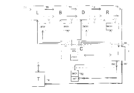
The arrangement illustrated in Figure
comprises a first device L, which applies solder paste
to printed circuit board blanks, a so-called dispensing
device D, a second device B, which is ~ormed by an
automatic population device and populates the printed
circuit boards, preferably using the SMD technique,
with one or more components or subassemblies, a third
device R, which is formed by a reflow soldering device,
an X-ray inspection device I, a data processing device
C, a repair workstation SST, which is also equipped for
the verification of defect-free printed circuit boards
(monitor SMON, which displays data generated by C) and
has a keyboard (not illustrated) for controlling the
monitor display or for carrying out dialogue with the
data processing device C, and also comprises a device T
which carries out electrical subassembly tests.
CA 0223684~ l998-0~-06
- 5 -
The devices L, D, B, R, I and T are devices
which are known per se. The device L is, for example, a
product from the MPM company bearing the product
description Ultraprint; the device D is, for example, a
product from the 3000 series from the Cama/lot company;
the device B is, for example, an SMD automatic
population device from the Siemens, Quad, Fuji or
Panasonica MPM companies; the device R is, for example,
a furnace from the BTU company or an appropriate
product from the Elektrovert company; the device I is,
for example, a product from the NICOLET (NIS) company
bearing the product description CX13000/5000 and
MV6000, and the device T is, for example, a product
from the Hewlett Packard company bearing the product
description HP 3070.
The devices L, B, D, R, and the repair
workstation SST have assigned to them screen monitors
LMON, BMON, DMON, RMON and SMON, which are connected to
the data processing device C.
The data processing device C has assigned to it
a control program defining the process according to the
invention. It is indicated schematically in Figure 1
with its controller CPU and with a memory CMEM which,
inter alia, serves for the acceptance of the
information which is formed within the context of the
process according to the invention and to which access
is made in order to form this information. The data
processing device is connected to the devices L, D, B,
R, I and T. The data processing device C receives from
these devlces first data which relate to the printed
circuit boards treated in these devices, and/or second
data which relate to the devices themselves. The first
and/or second data can also be supplied by a device
(e.g. L) of the device (e.g. B) that is in each case
arranged downstream. The data processing device C
supplies the devices L, B, D and R with control or
regulation information which is formed as a function of
solder-joint-specific quality information and/or the
solder-joint-specific measured value information.
CA 0223684~ l998-0~-06
- 6 -
The monitors LMON, BMON, DMON, RMON and SMON
are supplied by the data processing device C with,
inter alia, solder-joint-specific quality information,
solder-joint-specific measured value information and,
if appropriate, statistical information about the
frequency of occurrence of defects. This information is
displayed on the monitors. Monitor displays of this
type are illustrated in Figures 6 to 8 and lO.
The transport path of the printed circuit
boards is designated in Figure 1 by TR. From the output
of the X-ray inspection device I, a first transport
path TRI leads to the device T; transported on this
transport path are printed circuit boards which have
been detected as defect-free by the X-ray inspectlon
device I or by the data processing device C. However,
provision may also be made for printed circuit boards
detected as defect-free to be supplied to the repair
station SST for the purpose of verifying the freedom
from defects.
In addition, a second transport path TR2 leads
from the output of the X-ray inspection device I to the
repair workstation SST; transported on this transport
path are printed circuit boards which are detected as
defective by the X-ray inspection device I or by the
data processing device C. Following the repair, the
printed circuit boards can be transported back on the
transport path TR2 from the repair workstation SST to
the X-ray inspection device I, where they are once more
subjected to an inspection.
The X-ray inspection device I is capable, in a
manner known per se, of forming solder-joint-specific
information, either the information "solder joint
defect-free" or the information "solder joint
defective" being formed for each solder joint. In
addition, the device I measures physical parameters of
the solder joints, such as geometrical dimensions
and/or the solder volume, and forms appropriate
measured value information. A plurality of items of
CA 0223684~ l998-0~-06
- 7 -
measured value information may be formed in relation to
each solder joint.
To this end, the device I has the appropriate
data-processing functionality; as an alternative to
this, the corresponding data processing is carried out
by the device C.
Overall, the arrangement illustrated in Figure
1 constitutes a control arrangement with which printed
circuit boards may be pre-treated with regard to their
population with electronic components, may be
populated, soldered and checked for their quality.
The solder-joint-specific quality information
and/or solder-joint-specific measured value information
which characterizes measured physical parameters of
checked solder joints is used for the repair of
checked, defective solder joints, for the verification
of checked solder joints and/or for the control of the
production of further solder joints on-line, that is to
say in the continuous production process in which the
solder joints are tested.
For instance, the solder volume of the solder
joints and/or the height at least of one meniscus of
the solder joints and/or dimensions of the contact area
of the solder joints on the printed circuit board are
measured, and the measured value information is formed
from these measured values.
In this connection, provision is further made
that, using the solder-joint-specific quality informa-
tion and/or using the solder-joint-specific measured
value information, a test is carried out for defective
solder joints as to what type o~ defect is present.
This testing may be performed by means of algorithms
which are known per se and which are described, for
example, in EP O 236 001 Bl. These defect types
include, for example, "cold solder joint" and
"incorrect positioning of a solder joint".
The device I forms so-called tag files, that is
to say files in which the defect messages for one
printed circuit board are contained.
CA 0223684~ l998-0~-06
- 8 -
The control program that is assigned to the
controller CPU of the data processing device C
allocates the defects detected to a defect type or a
defect class in each case. For instance, the defect
classes "solder paste defect", "population defect" and
"soldering defect" are provided.
For example, the defects "deficient solder" and
"excessive solder" are defects of the defect class
"solder paste defect"; the defect "offset of a
populated component" is a defect from the defect class
"population defect"; and "wetting defect" (solder not
correctly fused with the pin) is a defect from the
defect class "soldering defect".
A defective solder joint may have a plurality
of defects, so that such a solder joint may be assigned
to a plurality of defect types or defect classes.
Depending on the respective defect class
(solder paste defect, population defect, soldering
defect), the data processing device supplies the device
L, B or R with control information. If the data
processing device has detected, for example, a defect
from the de~ect class "solder paste de~ect", it adjusts
the device L. If the data processing device has
detected, for example, a defect from the defect class
"solder paste defect" and, in addition, a defect from
the de~ect class "population de~ect", it adjusts the
device L and the device B. The control information may
comprise, for example, a defect warning signal, which
can be displayed on the devices L, B or R or on the
associated monitors, or may comprise data which modify
the operation of the respective device. Examples of
this are changes to the quantity of solder paste
supplied in each case and changes to the temperature of
the soldering means.
A defect may have several causes. For instance,
the defect "deficient solder" may arise from a "solder
paste defect" (= defect during the application of
solder paste) and from a "population defect" (= defect
during population, for example component is offset in
CA 0223684~ l998-0~-06
_ g _
such a way that only part of the area (lead) that is
normally to be wetted of the component is supplied with
sufficient solder), so that in this case the defect
"deficient solder" has the two defect classes "solder
paste defect" and "population defect" assigned to it.
For predefinable points on the printed circuit
board to be tested, the device I forms at least one
measured value, it also being possible for provision to
be made for a plurality of measured values to be formed
for a specific point on the printed circuit board. For
each predefinable solder joint, the device I provides
an item of measured value information or a combination
("rule") of several items of measured value information
to the data processing device C.
The control program that is assigned to the
controller CPU of the data processing device C is
configured in such a way that each item of measured
value information is compared with a desired value
(defect limit value) or with a lower and upper limit of
a permissible range. The desired values (defect limit
values) or the limits o~ permissible regions are
predefinable or have a fixed relationship with a
statistical mean which has been given by a process
recognized to be good. Provision may be made for the
limit values to be able to deviate only by predefinable
ranges in a measured-value specific manner from the
respective statistical mean of a process recognized to
be good.
If a combination of items o~ measured value
information consists of three items of measured value
information, for example, then each of the three items
of measured value information is compared with its
associated desired value (defect limit value), which
must neither be overshot nor undershot, or with the
lower and upper limit value of a permissible range.
If the result is that each item of measured
value information of the combination of items of
measured value information does not overshoot the
associated desired value which must not be overshot, or
CA 0223684~ l998-0~-06
- 10 - '
does not undershoot the associated desired value which
must not be undershot, or lies within the limits of the
permissible range, then the ("first") solder-joint-
specific item of quality information "solder joint
defect free" is formed. Otherwise, the ("second")
solder-joint-specific item of quality information
"solder joint defective" is formed.
If the second item of quality information
"solder joint defective" is to be formed, that is to
say the measured value overshoots a permissible upper
limit value or if it undershoots a permissible lower
limit value, then, in relation to the relevant solder
joint, that item of measured value information that has
the greatest relative deviation from the respectively
associated limit value is ascertained.
If the result is that, for example, the second
item of measured value information of the combination
of items of measured value information has the
relatively greatest deviation from its associated
desired value, one and only one of the devices L, B, D
or R is adjusted, depending on this item of measured
value information.
Provision may be made for those two items of
measured value information of a combination of items of
measured value information which have the relatively
greatest deviations from their respective defect limit
value in each case to be ascertained. If, in the
example of the combination of items of measured value
information comprising three items of measured value
information, this applies to the first and the second
items of measured value information, then depending on
these two items of measured value information (first
and second items of measured value information), then
it is only the device L, B, D or R which is responsible
for the occurrence of the relevant defect which is
adjusted. It is also possible for a plurality of
devices L, B, D, R to be the cause of defects for the
occurrence of combinations of items of measured value
CA 0223684~ l998-0~-06
t
information. In this case, the appropriate devices are
adjusted.
Furthermore, it is also possible for three and
more items of measured value information of a combina-
tion of items of measured value information to beevaluated in this way, in order in each case to adjust
those devices L, B, D or R which are responsible for
the respective defect.
The defect limit or desired values are
predefinable and preferably correspond to the statis-
tical means of a process recognized to be good;
however, the defect limit or desired values may also
deviate from these means.
If, for example, the width of a predefinable
solder joint is x millimetres as a statistical mean (at
the peak of the Gaussian distribution), then it is
possible for x + a, x - b, l.lx, etc. to be provided as
defect limit values. It is thus possible for typical
defect characteristics to be filtered out. x may be
20 millimetres and the predefinable lower defect limit
value may be 16 millimetres (x = 4 millimetres). A
current measured value at 18 millimetres is then judged
as adequate. The relative deviation of the current
measured value from the defect limit value is then
(18-16)/18 x 100% = 11.11%.
As an example, a combination of items of
measured value information consists of the following
three items of measured value information:
Measured value information item measured_width (measured solder
1: joint width) = 22 millimetres
Measured value information item heel solder (amount of solder)
2: corresponding to 6000
standardized grey-value
components in a defined testing
window
Measured value information item heel pad delta (solder meniscus
3: height) = 1500 micrometres.
CA 0223684~ l998-0~-06
i
- 12 -
The statistical means are, for example,
in the case of measured value
information item 1: 20 millimetres
in the case of measured value information item 2:
10,000 standardized grey-value components
in the case of measured value information item 3: 3Q00
micrometres.
Hence, the greatest relative deviation results
for the measured value information item 3.
This measured value information item 3 is assigned a
first item of information which identifies the defects
"soldering defect" and "solder paste defect". Using the
first item of information, the devices L and R are
adjusted.
If, in the case of this example, the two items
of measured value information having the greatest
relative deviations are ascertained, then these are the
measured value information item 3 and the measured
value information item 2. This combination of the
measured value information items 3 and 2 is assigned a
second item of information which identifies the defect
"soldering defect". Using this second item of
information, the device R is adjusted.
If all three items of measured value informa-
tion from the combination are evaluated, this combina-
tion is assigned a third item of information which
likewise identifies the defect "soldering defect".
Using the third item of information, the device R is
likewise adjusted.
The first, second and third items of informa-
tion firstly indicate which of the devices L, B, D or R
is adjusted. In addition, the first, second and third
items of information in each case indicate a controlled
variable, that is to say operational parameter or
operational parameter changes of the respective device
(for example, an increase or reduction in the quantity
of solder paste to be applied, an increase or reduction
in the solder to be applied).
CA 0223684~ l998-0~-06
- 13 -
The three defect classes "population defect",
"solder paste defect" and "soldering defect" have a
plurality (for example the following) defect types
assigned to them:
"Wet.Gullw. A", (wetting of gullwing)
"Wet.J-leg B", (wetting of J-leg)
"Wet.quad.SMD C", (wetting of cuboidal
SMD)
"SMD_offset D",
"other_sol_def. E",
"not_soldered F",
"solder_brldge G",
"bent_away/up H", (connecting pin bent
away/bent up)
"SMD_offset I",
"other_sol_def. J",
"solder_beads K",
"INSUFF_TOE L", (thin solder joint)
"SMD_bubble V", (solder bubble)
In addition, provlsion may be made for the
detected defects or items of measured value information
to be assigned to a defect type - such as listed above,
for example - and for the defect types to be assigned
to a defect class (solder paste defect, population
defect, soldering defect).
The solder-joint-specific quality information
and/or the solder-joint-specific measured value
information which characterizes the measured physical
parameters of checked solder joints, and/or statistical
information about the frequency of occurrence of
defects are displayed on the monitors LMON, BMON, RMON
which are assigned to the devices L, B and R.
The data processing device C and the repair
workstation SST may, for example, be designed in the
following two variants:
CA 0223684~ l998-0~-06
;
- 14 -
1. PC variants
CPU HP Vectra VL2 4/66
HP Vectra VL2 5/60
Main memory 24 MB
Hard disk 500 MB
Swap 60 MB
Graphics card Ultra VGA 1024x768 pixels
10 Monitor 15" or 17"
Operating system Solaris x86 2.4
Network card 16-bit BNC, TP, AOI
Options
15 Input Numeric keypad
Trackball
RS-232 bar-code scanner
Light pointer Heeb OM-500
Royonic 500
20 Printer HP DeskJet 1200C/PS
HP LaserJet 5MP
Data backup Magnetic tape (QIC or DAT)
Magneto-optical disk drives
25 2. Workstation variants
CPU Sun SparcStation 4
Sun SparcStation 5
Main memory 32 MB
30 Hard disk 1 GB
Swap 60 MB
Graphics card 1024x768, 1152x900 pixels
Monitor 15" or 17"
Operating system Solaris 2.4
35 Network card incorporated
Options
Input 3 1/2" floppy disk drive
Numeric keypad
~ CA 0223684~ l998-0~-06
;
- 15 -
RS-232 bar-code scanner
Light pointer Heeb OM-500
Royonic 500
Printer HP DeskJet 1200C/PS
HP LaserJet 5MP
Data backup Magnetic tape (QIC or DAT)
Magneto-optical disk drives
The control program defining the process
according to the invention is, for example, a UNIX
application which is mounted on the Solaris operating
system from SunSoft.
The control program realizes, inter alia:
a) a display of the X-ray inspection results
generated by the device I;
b) a display of the defects found during the X-ray
inspection, step by step in a graphic repre-
sentation of the printed circuit board layout;
c) a display of the defects found during the X-ray
inspection, step by step with the aid of a
laser/light pointer on the original printed
circuit board;
d) a display of defects (accumulatlon of defects at
one or more points on the printed clrcuit board)
in a graphic representation of the printed circuit
board layout;
e) verification, acknowledgement and further process-
ing of the defects found during the X-ray
inspection, if necessary step by step by an
operator o~ the repair workstation SST, using a
dialogue menu; and
CA 0223684~ l998-0~-06
- 16 -
f) storage of processed defect data as an interface
to a program module (defined in Claim 8) or to
quality management systems.
The abovementioned elements of the control
program are described below:
a) display of the X-ray inspection results generated
by the device I in text form.
This display is produced on the SMON monitor of
the repair workstation SST.
The program working area comprises a main
window with a menu bar. Further windows may be
superimposed.
The menu bar comprises the following menus with
the options:
~ File File functions
Editor Call up a text editor
Exit Exit from program
~ Operating mode Select operating modes
Individual de~ect Individual defect display
De~ect overview Display of the defect over-
view
X-ray image Display of the X-ray image
~ Configuration Configuration settings
Light/laser pointer> Select the light/laser
pointer
Royonic 500 Royonic 500 light pointer
Heeb laser Heeb LL-2A or OM-500
Operating mode> Setting the standard
operating mode(s)
Individual de~ect Individual defect display
Defect overview Defect overview
X-ray image X-ray image window
CA 0223684~ l998-0~-06
- 17 -
File paths> File path specification
CXI tag files Path to the CXI tag files
X-ray image files Path to the X-ray views
-CAD files Path to the CAD files
Results files Path to the results files
Defect type reference Path to the defect type
reference file
Verification dialogue>
GOOD boards auto. Automatically accept
defect-free boards
Options> Option menu for various
settings
Symbol bar Superimpose and hide symbol
bar
Save on exit Save settings on exit
The above-described menu bar is- adapted
appropriately in the event of changed or additional
operating steps.
b) Display of the defects found during the X-ray
inspection, step by step in a graphic
representation of the printed circuit board layout
bl) Operating mode: individual defect display
The control of the individual defect display by
the operator o~ the repair workstation SST is carried
out using a dialogue window, which contains the
elements
~ Header,
~ Option group Display,
~ Option group Page,
~ Defect list,
~ Buttons, Next, Back, True defect, Pseudo defect,
New defect, Change defect type, Next component,
Done, Abort
CA 0223684~ l998-0~-06
- 18 -
In the "Header", the data from the top of the
data from the X-ray system I are displayed.
Using the "Option group Display", the operator
is able to select the display forms for the individual
defect display. The options available are "Layout", for
the representation of the graphical printed circuit
board layout on the monitor, and "Pointer", for the
display on the original printed circuit board with a
light/laser pointer.
With the aid of the "Option group Page", the
side of the printed circuit board that is displayed is
selected. Those available are upper side and lower
side.
The "defect list" contains all the defects on
the printed circuit board that were found by the X-ray
system or added by the operator. The defect which is
currently displayed in the printed circuit board layout
and/or indicated by the light/laser pointer is
highlighted in the defect list.
The button "Next" displays the next defect in
the defect list in the printed circuit board layout
and/or using the light/laser pointer.
The button "Back" displays the preceding defect
in the defect list in the printed circuit board layout
and/or using the light/laser pointer.
The button "True defect" marks the current
defect as a true defect.
The button "Pseudo defect" marks the current
defect as a pseudo defect.
The button "New defect" inserts a new defect
into the list and shows the defect in the printed
circuit board layout and/or using the light/laser
pointer.
The button "Change defect type" permits the
defect type of a defect that has already been marked to
be changed again.
The button "Next component" jumps to the next
component in the defect list. If this button is
pressed, the individual defects are erased, and the
, CA 0223684~ 1998-0~-06
;
- 19 -
defect code for the total component defects is entered
in the results file.
The button "Done" or the button ''Enter" after
the last defect entry enters the marked true defects
and the marked pseudo defects in the results file and
terminates the verification operation for this
subassembly. In the event of a premature abort, an
abort message is entered ln the results file as the
last line (see also the "Abort" button).
The button "Abort" closes the dialogue window
and the window with the graphical printed circuit board
layout and/or moves the light/laser pointer into a rest
position. An abort message is entered in the results
file (see below) as the last line.
Via a standardized software interface, the
selected defect is transferred to the program module
for the display in the graphical printed circuit board
layout and using the light/laser pointer.
If the display of the printed circuit board
layout is activated, then each defect in the defect
list is displayed by means of a marking in a graphical
printed circuit board layout, which is produced from
CAD data that describe the printed circuit board. A
display is illustrated in Figure 2, it being the case
that, for example, the solder joint marked by the
(external) arrow in the actual screen display is
assigned a marking which cannot be seen in Figure 2.
In a standard setting, all the subassemblies of
the printed circuit board are displayed in the
graphical layout. Defect data are accepted via a
standardized software interface, and the appropriate
defects are displayed. Defects are highlighted in
colour.
It is possible to display the entire printed
circuit board or only a detail, preferably on an
enlarged scale.
CA 0223684~ l998-0~-06
- 20 -
b2) Operating mode: defect overvlew
This operating mode makes it possible to display
the marked true defects from the defect list,
together or separated by defects, on a graphical
representation of the printed circuit board
layout.
The defeGts which the device I detects are
assigned to the defect types "population defect",
"soldering defect" and "solder paste defect".
"Population defects" are displayed in blue, "soldering
defects" in yellow and "solder paste defects" in green.
The side (upper side/lower side) of the printed circuit
board on which the components are located is indicated
in the window.
Illustrated in Figure 3 is an example of a
de~ect list displayed on the screen.
b3) Operating mode: X-ray image display
In a separate window, it is possible for the X-ray
image matching the data generated by the device I
to be displayed. An example of such a window is
illustrated in Figure 4, a defective solder joint
on the right in the window being marked by a
square frame. It is optionally possible for the
complete components list of the image to be
superimposed on this window.
c) Display of the defects found during the X-ray
inspection, step by step with the aid of a
laser/light pointer on the original printed
circuit board;
If the display using the light/laser pointer is
activated in the dialogue window, then the defect
is indicated on the original printed circuit board
using a point of light. For example, it is
possible to use the Royonic light pointer 500 or
Heeb Laserlite LL-2-A or 500 light/laser pointers.
e CA 0223684~ l998-0~-06
- 21 -
d) Display of defects (accumulation of defects at one
or more points on the printed circuit board) in a
graphical representation of the printed circuit
board layout.
An example of a display of this type is
illustrated in Figure 5, it not being possible in
Figure 5 to recognize the actual defect data which, in
the actual screen display, are assigned adjacent to the
associated solder joints.
Further displays of defects in a statistical evaluation
are illustrated in Figures 6, 7 and 8.
e) Verification, acknowledgement and further process-
ing of the defects found during the X-ray
inspection, optionally step by step by an operator
of the repair workstation SST using a dialogue
menu.
The sequence of a cycle in conjunction with the
verification of defect-free printed circuit boards, and
the repair of defective printed circuit boards, is
described below, and is also illustrated in Figure 9.
For the verification and repair of printed
circuit boards, it is necessary for the individual
defect display operating mode to be activated. A repair
cycle begins with reading the printed circuit board
number using a bar-code reading pen.
Alternatively, the repair may also begin with
the selection of a defect tag file via keyboard or
mouse.
On the basis of the printed circuit board
number read, the associated tag file for the printed
circuit board is sought and opened, and the header and
the defect list are read. If a defect-free printed
circuit board is involved, then a distinction is made
between two cases, depending on the GOOD_BOARDS switch:
CA 0223684~ l998-0~-06
- 22 -
~ GOOD_BOARDS-AUTO
A message is displayed to say that the printed
circuit board is defect free, and an entry in the
results file is automatically generated, or a new
results file is created, in which the defect-free
printed circuit board is noted.
~ GOOD_BOARDS=MANU
The procedure continues as in the case of
defective printed circuit boards, with the
exception that the defect list is empty.
In the case of a defective printed circuit
board, on the basis of the subassembly identification
number contained in the header of the tag file, the CAD
files are sought and opened and the geometric data of
the subassembly are read. If the subassembly
identification number of the current printed circuit
board is identical with that previously tested, then
the renewed reading of the geometric data is omitted.
The defect list is displayed in the dialogue
window, the first defect is marked and indicated on the
printed circuit board layout on the screen and/or using
the light/laser pointer.
With the aid of the switching areas in the
dialogue window that were described in the section
"individual defect display", the defects in the list
can then be classified and marked by the operator.
After a defect has been marked, a jump is automatically
made to the next defect. If the operator has marked
(processed) all the defects in the list, or marked them
as a total defect using "next component", then these
defects are entered in the results file.
Following the processing of the board, the test
files relating to the printed circuit board (I-tag
files, X-ray images) are removed, if a switch
DEL_TAG=On is set. The standard value is DEL TAG=Off.
If there is no test tag available for the
current board, the results file is looked through
CA 0223684~ l998-0~-06
- 23 -
following an entry for this board or the corresponding
directory is looked through for a results file for this
board, and the following is done:
5 ~ Output of a defect message if the board is also
not present in the results file or 1~ no dedicated
results file exists for this board.
~ If a defect-free board is concerned, from which
the tag file is available, then the procedure is
as described above, depending on the GOOD_BOARDS
switch.
~ If the renewed processing of the board is
concerned (no tag file, but entry in the results
file or a dedicated results file), then the
further operation is affected by the REWORK_BOARDS
switch. If the entry in the configuration file is
REWORK_BOARDS=On, then the printed circuit board
can be processed once more using the defect data
from the results file. If, on the other hand, the
entry is REWORK_BOARDS=Off, then a message is
output that repeated processing is not possible.
f) Storage of processed defect data as interface to a
program module (defined in Claim 8) or to quality
management systems.
The data processing device C processes, inter
alia, population data, using the following fields:
=
CA 0223684~ 1998-0~-06
- 24 -
Field name Data ~ormat Description
Joint long int Consecutive number of the
solder joint (I to
max joint)
Pin/Device long int Consecutive number of the
pin per component (1 to
max pin)
Pin X long int X-coordinate of the pin
related to the board origin
Pin Y long int Y-coordinate of the pin
related to the board origin
Pad X long int Pad length in X-direction
Pad Y long int Pad length in Y-direction
Side char Subassembly side (T I B)
Device name char[15] Designation of the component
(without '\O')
Device type char[25] Designation of the component
type (without '\O')
View long int Consecutive number of the
view (1 to no of views)
View X long int X-coordinate of the pin in
relation to the view
View Y long int Y-coordinate of the pin in
relation to the view
In addition, the data processing device C
processes a defect type reference file.
As already described, each defect detected by
the device I is assigned a defect class "population
defect", "soldering defect" and "solder paste defect".
The contents of the file are organized into individual
data sets having, for example, four data fields. Each
line of the file describes one reference. The fields
have the following meanings:
CA 0223684~ 1998-0~-06
- 25 -
Field name Field length Description
De~ect 3 characters Defect number
(long)
De~ect -s~e 20 characters As per defect tag
De~ect class 3 characters Defect class
(long)
De~ect class 20 characters Message for screen outputs
message
Colour 10 characters Colour with which this defect
is displayed on the screen
Sy~bol 10 characters Symbol that is used to display
the defect on the light/laser
pointer
An example of a defect type reference file is
configured as follows:
#Defect type Defect class Colour Symbol
ff
65;2503 solder link a;1;soldering defect; yellow; point
40;2503_Wet.Gullw. H;1;soldering defect; yellow; point
18;3208 offset row 2;4;population defect blue; arrow
For each printed circuit board, a dedicated
results file may be generated. As an alternative to
this, a common results file can be generated for a
plurality of processed printed circuit boards, in
particular for all processed printed circuit boards.
For the two types of results file, each defect
generates an entry in this file.
For the subassembly handled, a header dataset
is created first, this consisting of the following
fields:
CA 0223684~ l998-0~-06
- 26 -
Field nam~ Field length Description
Data~et Ly~e 1 character alway3 "H" in header
line
Serial num-ber o~ the 25 character~ as per defect tag or
8ll~a~- ~ly bar-code
Blank ID 2 character~ (long) a~ per defect tag
Subassembly type 20 characters a~ per defect tag
Test system ID 12 character~ a~ per defect tag
Date o~ inspection dd:mm:yy a~ per defect tag
Time o~ inspection hh:mm:~ a~ per defect tag
UserID o~ tester 4 character~ (long) as per/etc./pa~wd
file
Date o~ repair dd:m~:yy as per ~y~tem time
T;~ o~ repair hh:mm:qs a~ per ~ystem time
Status 1 character (long) 0 = no repair; 1, 2
number of repair~
Adjacent to this header line there follows, for
each defect, a data line which consists of the
following fields.
Field nam-e Field length Description
Data~et type 1 character alway~ "D" in data
line
C, _-n~t name 15 character~ a~ per defect tag
Pin nllm~er 3 characters (long) a~ per defect tag
De~ect code 1 3 character~ (long) a~ per defect code
table
De~ect code 2 3 character~ (long) a~ per entry by the
te~ter
Rule 2 characters (long) as per defect tag (D1
field)
De~ect cla~s 3 characterq (long) a3 per reference table
De~ect ~tatus 2 character~ (long) Code (0 = confirmed, 1
= changed, 2 = p~eudo)
CA 0223684~ l998-0~-06
- 27 -
The above-described process may be one control
program from a plurality of program modules assigned to
the controller CPU. The control program, which is
preferably of modular construction, may have further
program modules which are the subject-matter of the
subsidiary Claims 5, 8 and lO and of the claims that
are dependent on these. Each program module can be used
on its own or together with one or more other program
modules.
A program module of the control program is, as
already described, configured in such a way that the
X-ray images generated by the device I, or electronic
images generated from these and images generated from
CAD data and relating to the graphical layout of the
printed circuit boards may be displayed on the monitor
SMON at the repair workstation SST.
In this case, the X-ray images or the
electronic images, as well as the printed circuit board
layout images are displayed together with solder-joint-
specific measured value information which characterizesmeasured physical parameters of checked defective
solder joints, optionally together with statistical
information about the frequency of occurrence of
defects. The information is displayed alphanumerically
and/or symbolically in the X-ray images.
A further program module of the control program
is configured in such a way that the solder-joint-
specific quality information and/or solder-joint-
specific measured value information which characterizes
measured physical parameters of checked solder joints,
is compared with predefinable production process
threshold values and that, depending on the comparison,
process control data are formed. For example, the
production process threshold value predefined is a
specific amount of solder which is to be applied per
predefinable solder joint. If, using a comparison of
this production process threshold value or production
process reference value with the corresponding solder
amount measured value information, the result is that
CA 0223684~ l998-0~-06
- 28 -
this threshold or reference value is overshot or
undershot by a predefinable tolerance range, the data
processing device C forms alphanumeric and/or graphical
information which describes the reference value and/or
the measured value information and/or the extent of
overshooting or undershootlng the reference value.
Furthermore, the data processing device may determine
that (those) device(s) (L, B, R) which cause(s) the
overshooting or undershooting of the amounts of solder.
This information is fed to the monitor SMON of the
repair workstation SST and to the monitor of that
device (e.g. R) which is causing the overshooting or
undershooting of the amounts of solder. Appropriate
screen displays are illustrated in Figure 10.
Furthermore, the data processing device C may
form an item of control information for this device
(e.g. R) which effects a change in the operating
parameters of this device. If, for example, the
reference value is exceeded to a certain extent, then
the control information (that is to say process control
data) are formed in such a way that the device R
reduces the amount of solder per solder joint
appropriately. These procedures, which are carried out
for the direct control of the continuous production
process, may already be carried out on-line before the
occurrence of soldering defects, that is to say at
times at which "solder joint defect free" quality
information is still being formed.
Screen displays in conjunction with the
configuration of measured values and of reference
values ("upper warning limit", "lower warning limit")
are illustrated in Figures 11 to 14.
Using the solder-joint-specific quality
information and/or using the solder-joint-specific
measured value information, a test is therefore carried
out, for solder joints whose physical parameters
deviate from the predefinable production process
threshold values or reference values, as to which of
the first and/or the second and/or the third devices L,
CA 0223684~ l998-0~-06
- 29 -
B, R this deviation is to be assigned. Depending on
this assignment, the first and/or the second and/or the
third devices (L, B, R) and, if appropriate, also the
associated visual display device (LMON, BMON, RMON) are
adjusted using the process control data. The display
devices are, in particular, fed with the alphanumeric
and/or graphical information that is formed by the data
processing device C and which characterizes the
reference value and/or the measured value information
and/or the extent of the overshooting or undershooting
of the reference value.
A further program module is configured in such a
way that the solder-joint-specific quality information
and/or the solder-joint-specific measured value
information which characterizes measured physical
parameters of checked solder joints is correlated with
grey-value parameters of X-ray images of the solder
joints and, on the basis of the correlation, criteria
for the formation of the solder-joint-specific quality
information and of solder-joint production process
threshold values are generated.
That is to say, rules for the formation of the
solder-joint-specific quality information and of
solder-joint production process threshold values are
generated. The starting point is the measured value
information from defect-free and defective printed
circuit boards, these data being treated statistically,
as well as component-specific parameters which are
stored in a scaling library.
As already described, the device I measures
physical parameters of the solder joints, for example
geometric dimensions or the profile of the solder
joints. One profile parameter, or preferably several
profile parameters, such as two height points on the
meniscus, the difference between these height points or
between each of the height points and the lowest point
on the solder joint surface, or a vertical cross-
sectional area of the solder joint is or are selected.
These profile parameters of solder joints of
-
CA 0223684~ l998-0~-06
- 3~ -
particularly good or particularly poor quality are
combined or correlated with grey-value parameters of
the X-ray images of the corresponding solder joints. As
a result, automatically determined profile parameters
and limit values are selected, these forming new
decision criteria for future assessments of the quality
of solder joints.
Within the context of the process according
to the invention, therefore, solder-joint-specific
measured value information is evaluated on-line and
transmitted to different devices in the production
process. X-ray defect images are used on-line at the
repair workstation. Quality information, specifically,
inter alia, measured value information, are assigned to
the individual production steps or the corresponding
devices and displayed there. As a result of the
feedback of this information, the production process is
controlled. Furthermore, layout-oriented statistics are
generated on-line. Finally, using component-relevant
data and statistically treated measured value
information, rules relating to the solder-joint type
are defined for the detection o~ soldering defects and
process limit values.