Note : Les descriptions sont présentées dans la langue officielle dans laquelle elles ont été soumises.
CA 02240178 1998-06-10
CAPACITIVE DATA CARD AND READER THEREOF
TECHNICAL FIELD
The present invention relates to an improvement of a
capacitive data card in which a fuse is built in a circuit
thereof and a bit of data is represented by a state of the
fuse, and also relates to a reader of the capacitive data
card.
TECHNICAL BACKGROUND
It is convenient for a user to use a data card
(hereafter, refer to a prepaid card) in which no change in
payment is required in many application examples such as a
public telephone, a parking meter, an automatic vending
machine and traffic facilities. No cash is used in a
device receiving the card so that damages such as
destruction for the purpose of a theft, etc. are avoided.
Therefore, there are advantages of lengthening a device
life, etc.
Among such prepaid cards, a capacitive data card
constituting one portion of a circuit having a capacitor
comes to public notice as a data card with low price and
low energy. A prepaid card system of this capacitive type
is already registered as U.S. Patent No.4280119 on July 21,
1981.
International Application W095/14285 of May 26, 1995
discloses a prepaid card system with a fuse built in a
CA 02240178 1998-06-10
circuit of the capacitive data card. When this fuse is
intact, the fuse is in a state in which an electric current
flows through this fuse. When the fuse blows out,
resistance of the circuit is substantially increased.
Therefore, a bit of data is represented by a resistance
state of the fuse.
As shown in FIG.14, this capacitive data card can
form a circuit 3 having capacitors only when a card section
1 is integrated with a sensor section 2 formed on a reader
side.
This card section 1 has a resistor Rl and electrode
portions la, lb each forming one portion of a capacitor
connected to each terminal of this resistor Rl. A sensor
section 2 has electrode portions 2a, 2b each forming one
portion of the capacitor connected to each terminal of a
power source 4. When the card section 1 is set to the
sensor section 2, a circuit having air capacitors 3a, 3b
having air between the electrode portions is formed as
shown in FlG.14.
When the resister Rl in the circuit 3 formed as
mentioned above is burned out by flowing an electric
current having a high voltage through the resistor Rl, the
resistor Rl is used up and a state of the resistor Rl which
is not burned out represents an unused bit so that one
closed circuit provides a signal of one bit. Therefore, it
is possible to form a data card in which a signal having a
required digit number can be stored by forming an arbitrary
CA 02240178 1998-06-10
number of closed circuits.
However, in the above conventional capacitive data
card, bits are changed from an unused state to a used state
by burning out the resistor Rl so that data cannot be
easily regenerated. Accordingly, since data are not easily
regenerated, alteration of the data is prevented and the
capacitive data card has high reliability as merits.
However, a constant limit is imposed on update of data
stored in the card so that a problem exists in that utility
value of the card cannot be sufficiently fulfilled.
In consideration of such a situation, the present
invention provides a capacitive data card with high utility
value and high reliability, and also provides a reader of
this capacitive data card.
DISCLOSURE OF THE INVENTION
To achieve the above object, a capacitive data card
according to claim 1 comprises a capacitive memory area for
storing bits relative to capacitive data in accordance with
a resistance state of a fuse which is built in a circuit of
the card, that is, a state for flowing an electric current
through the circuit is set when the fuse is intact, and
resistance of the circuit is substantially increased when
the fuse blows out, and a magnetic memory area for storing
magnetic data.
Further, the above mentioned capacitive memory area
comprises a rough estimate remaining means which shows a rough
CA 02240178 1998-06-10
estimate of the remaining amount of compensation recorded in the
card by a bit.
A capacitive data card according to claim 2 comprises
a capacitive memory area for storing capacitive data and a
magnetic memory area for storing magnetic data, and a layer
constituting the magnetic memory area is provided on the
surface of a substrate having the shape of a thin plate,
and a layer constituting the capacitive memory area is
superposed on a surface of the layer constituting the
magnetic memory area.
A capacitive data card according to claim 3 comprises
a capacitive memory area for storing capacitive date, and a
magnetic memory area for storing magnetic data, and a layer
constituting the capacitive memory area is formed on one
side of a substrate having the shape of a thin plate, and a
layer constituting the magnetic memory area is formed on
the other side of the substrate. In this case, according
to claim 4, a coating layer in the shape of a thin film
which is made of a polyethylene film, etc. is desirably
superposed on both of the surface of the capacitive memory
area layer and the magnetic memory area layer to prevent
warp of the substrate.
According to claim 5 of the present invention, the
capacitive data card may have a construction in which data
stored in the magnetic memory area are stored into a well-
CA 02240178 1998-06-10
known IC chip.
On the other hand, a capacitive data card reader according
to claim 6 comprises a first input output means for storing data
in the capacitive memory area of the capacitive data card or
reading the data stored therein, a second input output
means for storing data to the magnetic memory area or
reading the data stored therein, and a checking means for
judging that the card is invalid irrespective of the data
stored in the magnetic memory area when data read from the
capacitive memory area are predetermined data.
BRIEF DESCRIPTION OF THE DRAWINGS
FlG.l is a view showing a capacitive data card in
accordance with a first embodiment of the present invention.
FIG.2 is a block diagram showing the circuit
construction of a capacitive memory area in accordance with
this embodiment.
FlG.3 is a view showing an input output section of a
capacitive data card reader in accordance with this
embodiment.
FIG.4 is a block diagram showing the construction of
CA 02240178 1998-06-10
a processing section relative to an input and an output of
the capacitive data card reader in accordance with this
embodiment.
FIG.5 is a block diagram showing processing of a CPU.
FlG.6 is an exploded perspective view showing a
capacitive data card in accordance with a second embodiment
of the present invention.
FlG.7 is a longitudinal sectional view of the same
capacitive data card.
FIG.8 is an enlarged longitudinal sectional view of
a capacitive memory area of the same capacitive data card.
FlG.9 is an enlarged longitudinal sectional view of
a capacitive data card in accordance with a third
embodiment of the present invention.
FIG.10 is an enlarged longitudinal sectional view of
a capacltive data card in accordance with a fourth
embodiment of the present invention.
FIG.ll is a view showing the mechanism of a card
reader in accordance with a fifth embodiment of the present
invention.
FIG.12 is a block diagram showing an input output
section of the same card reader.
FlG.13 is a block diagram showing processing of a
CPU section of the same card reader.
FIG.14 is a conceptual explanatory view
schematically showing a basic capacitive data card system.
CA 02240178 1998-06-10
BEST FORMS FOR EMBODYING THE INVENTION
First embodiment
The embodiments of the present invention will be now
explained with reference to the drawings.
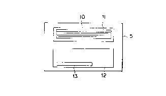
FIG.l shows a capacitive data card 5 in accordance
with a first embodiment of the present invention. This
card 5 has a capacitive memory area 12 relative to storage
of capacitive data and a magnetic memory area 10 relative
to storage of magnetic data, and is normally used as a
~prepaid card".
Magnetic tracks 11 are formed in the above magnetic
memory area 10 in reading and writing directions of the
card 5. Although, the number of magnetic tracks 11 is set
to three in this embodiment, it is not limited to three and
many vary according to a memory amount depending on a use
purpose of the card 5.
Data are stored in the above tracks 11 in an
information character order. A cyclic redundancy check
code (CRC code) for a reading check is formed in recorded
effective data. For example, magnetic characteristics and
an information recording format in the magnetic memory area
10 may be based on Japanese Industrial Standard (JIS).
In regard to the above capacitive memory area 12, a
plurality of first electrodes 31 are arranged in one line on one
surface of the card 5 and second electrodes 32 formed in a strip
shape are arranged on the other surface of the card 5 in a
parallel position to the first electrodes 31 as shown in FIG.
2, such that this arrangement is in conformity with an electrode
arrangement of an input output section 6 (see FIG. 3 and FIG.
CA 02240178 1998-06-10
4) described later. An elongated second electrode 32 is
arranged on the surface of the capacitive memory area 12 in
parallel with the line of the first electrodes 31.
Each of the first electrodes 3 is connected to the
second electrode 32 through a fuse 33. When this fuse 33
is intact, an electric current freely flows between each of
the first electrodes 31 and the second electrode 32, and a
very small resistance state is set. When the fuse 33 is
burned out, an increase in resistance sufficient to reduce
the flow of the electric current is caused.
Generally, card information recorded on the "prepaid
card" has two types of information, i.e., fixing
information not rewritten and variable information
rewritten in a card use, etc.
The above fixing information includes "card issuer
number", "card issuing date", "nominal value of card", "the
term of validity of card", "card usable data (a code
written to show that the card is usable at the time of
issuing card)", "password number (a number for recognizing
by the system that a card user is the registered person)",
and the like. The variable information includes "the card
previous balance (the balance before settlement of
accounts)", "the card new balance (the balance after
settlement of accounts)", "used device number (device
number of settlement of accounts)", "used store (store
number of settlement of accounts)", and the like. For
example, in the case of an amount of money, the card
CA 02240178 1998-06-10
balance is shown by frequency such as a telephone card
depending on a use purpose of the card.
In this embodiment, the above fixing information is
recorded on both the magnetic memory area 10 and the
capacitive memory area 12. Further, a rough estimate
remaining memory section 13 showing a rough estimate of the
remaining amount of card compensation is provided in the
capacitive memory area 12.
In one example of using this rough estimate remaining
memory section 13, for example, when the nominal value of
the prepaid card is one thousand yen, 10 fuses (10 bits)
relative to capacitive data are secured and are
sequentially blown out (burned out) in a predetermined unit
in accordance with a reduction in the balance at the time
of using the card 5. In a state in which all the fuses 33
blow out, the balance is set to zero and value of the card
5 is lost.
When the fuses are burned out, a boundary area around
the fuses is heated so that the rough estimate balance can
be visually confirmed by applying a material having a color
changing property by heat in a corresponding portion.
The above variable information is recorded on the
above magnetic memory area 10 in addition to the above
fixing information. Among the variable information, the
"card new balance (balance after settlement of accounts)"
is particularly important which shows the value of the card
5. Therefore, in this embodiment, this "card new balance"
CA 02240178 1998-06-10
and the ~rough estimate balance" of the above rough
estimate remaining memory section 13 are updated in
association with each other.
For example, the card new balance is updated in the
same one-yen unit as an adjusted amount at every use of the
card 5. On the other hand, with respect to the rough
estimate remaining memory section 13, the fuses blow out in
one hundred yen unit and the rough estimate balance
decreases in amount. In this case, for example, if an
amount of money equal to larger than the card new
balance is stored as the rough estimate balance, it is
possible to check the prepaid card as invalid when the card
new balance is larger than the rough estimate balance, or
when the rough estimate balance is zero but the card new
balance is left.
It is not necessary to update the rough estimate
balance by the unit of constant amount of money. If a unit
of the "updated amount of money" is set to be smaller as
the balance is reduced, it is convenient for a demander to
visually confirm the above rough estimate balance.
In addition to the fixing information and the
variable information described above, for example, various
kinds of information depending on a use purpose such as
information of a passenger interval of traffic facilities,
a utilizing interval of a superhighway, etc. can be
recorded on the magnetic memory area 10.
Next, the reader of the above card 5 will be
CA 02240178 1998-06-10
explained. As shown in FIG.3, the input output section of
the reader of this card 5 comprises a card feed base 21,
feed rollers 22, a card taking-in motor 23, a magnetic head
19, a cushion rubber case 8, a taper prate 8a, a lever 26,
a solenoid 27, and an edging sensor 28 or an optical sensor
29. The card feed base 21 puts the card 5 thereon and
feeds the card 5 until a position capable of performing
reading and writing operations. The feed rollers 22 are
arranged as a feed device for moving the card 5 until the
position capable of performing the reading and writing
operations by applying moving force to the card 5 above
this card feed base 21. The card taking-in motor 23
supplies rotating power for rotating these feed rollers 22.
The magnetic head 19 performs the reading and writing
operations of magnetic data with respect to the magnetic
memory area 10. The cushion rubber case 8 is arranged just
above the input output section 6 arranged at a terminal end
of the card feed base 21 and functions as a pressing member
for pressing the card 5. The taper plate 8a is arranged as
a pressing direction converting member of a pressing means
arranged on an upper face of this cushion rubber case 8.
The lever 26 is arranged as an arm portion of the pressing
means to which rollers 25, 25 for pressing this taper plate
8a from above are attached. The solenoid 27 is arranged as
an operating portion of the pressing means for operating
this lever 26. The edging sensor 28 or the optical sensor
29 is arranged as a detecting means for detecting that the
CA 02240178 1998-06-10
card reaches an end edge portion of the input output
section 6.
As shown in FlG.4, an interface pad 41 is arranged
in the above input output section 6 in a card inserting
position. On this interface pad 41, first electrodes 42
are arranged in one line and the number of first electrodes
42 is set to be equal to the number of first electrodes 31
of the above card 5. Further, similar to the second
electrode 32 of the above card 5, a second electrode 43 is
formed in an elongated shape. The electrodes 42 and 43 are
arranged on a pad surface in positions corresponding to the
respective electrodes 31 and 32 such that the electrodes 42
and the electrodes 43 can be respectively connected to the
first electrodes 31 and the second electrode 32 of the card
5.
The first electrodes 42 and the second electrode 43
are respectively connected in parallel to a switch network
44. This switch network 44 selectively switches supply
destinations of an analog voltage to be supplied and
supplies a required voltage to selected one of the
electrodes 42 or the electrode 43.
Further, a voltage generator 45 and a power source 47
are arranged in the above input output section 6 in
addition to the first electrodes 42,the second electrode
43 and the switch network 44. The voltage generator 45
supplies the required voltage to each of the first
electrodes 42 or the second electrode 43 through this
12
CA 02240178 1998-06-10
switch network 44, and detects an output voltage. The
power source 47 supplies a required voltage to each device
of the input output section 6 and a read write driver 48
for controlling an operation of the magnetic head 19.
The operation of the input output section 6 having
the above construction is controlled by a CPU 46. As shown
in FlG.5, this CPU 46 has a capacitive reading processing
section 51 for controlling reading and writing operations
of capacitive data, a magnetic reading writing processing
section 52 for controlling reading and writing operations
of magnetic data, a data checking section 53 for checking
data contents, etc., and a control section 54 for generally
controlling operations of these sections.
An operation of the above reader will next be
explained. When a card 5 is inserted into the input output
section 6 from the card feed base 21, the rollers 22, 22
rotated by the card taking-in motor 23 give moving force to
the card 5 from its rear face so that the card passes
through the magnetic head 19. In this case, this magnetic
head 19 reads magnetic data from a track 11 of the card.
These magnetic data are transmitted to the magnetic reading
processing section 52 through the read write driver 49.
Subsequently, when the above card 5 is fed and reaches the
input output section 6, the edging sensor 28 or the optical
sensor 29 detects that the card 5 is inserted in a
predetermined position. Thus, the solenoid 27 is turned on.
When the solenoid 27 is turned on, this solenoid 27
13
CA 02240178 1998-06-10
moves the lever 26 in an operating direction thereof so
that the lever 26 is rotated around a pin 26a as a center.
Thus, the rollers 25, 25 are rotated so that the taper
plate 8a is moved in an increasing direction in height.
While a taper face is pressed, the cushion rubber case 8 is
pressed downward and uniform pressing force is applied to
the card 5 through the cushion rubber.
When it is detected that the card 5 has thus reached
The input output section 6 and the card 5 is inserted in a
predetermined position, a signal is outputted to the switch
network 44 and the CPU 46 and it is informed that readable
and writable states are set. Thus, a closed circuit having
air capacitors is formed between the card 5 and the input
output section 6, and the reading and writing operations of
data can be executed by the input output section 6.
At the time of reading the above data, a signal is
outputted to a pair of first electrodes 42, 42 connected to
the above second electrode 430n the basis of a reading
control signal from the capacitive reading processing
section 51 so that "an electrode through which an electric
current flows" is designated. The electric current then
flows through this electrode and information of a bit
thereof is read. This procedure is repeated and all second
electrodes 43 and all pairs of first electrodes 42, 42
connected to these second electrodes 43 are designated and
an electric current flows through these electrodes so that
all registered contents of the card 5 are read.
14
CA 02240178 1998-06-10
When the reading operation of the card 5 is
terminated, the data checking section 53 checks in the
following procedures whether the data contents are right.
First, it is confirmed whether all bit data in the
rough estimate remaining memory section 13 show zero
(showing that fuses are melted and cut). When all the bit
data show zero, it is judged that value of the card 5 is
vanished. Accordingly, measures for collecting the card 5,
etc. are taken by an unillustrated collecting mechanism.
In this case, contents of the "card new balance" stored in
the magnetic memory area 10 are neglected as invalid data.
The "card new balance" of the magnetic memory area 10
and the "rough estimate balance" in the rough estimate
remaining memory section 13 are also compared with each
other. When the "card new balance" is larger than the
"rough estimate balance", this card is judged as an invalid
card and measures for collecting this card, etc. are taken.
In this case, as mentioned above, it is set as a premise
that the card is managed such that the "rough estimate
balance" is equal to or greater than the "card new balance"
at any time.
Further, if necessary, fixing information stored in
the magnetic memory area 10 and fixing information stored
in the capacitive memory area 12 and corresponding to this
fixing information are compared with each other. When
these fixing information do not agree with each other, this
card is set to a bad card and predetermined measures for
CA 02240178 1998-06-10
this card are taken. In particular, magnetic data in the
magnetic memory area 10 tend to be easily influenced by
magnetism and there is a possibility that the magnetic data
are easily erased, etc.
When the card 5 is judged as an effective card as a
checking result, this card 5 functions as a prepaid card
and a card amount adjustment is made so that the "card new
balance" and the "rough estimate balance" are newly
respectively written to the magnetic memory area 10 and the
capacitive memory area 12.
Data are also written to the card 5 in addition to
this adjustment. A second electrode 43 and a pair of first
electrodes 42, 42 connected to this second electrode 43 are
designated on the basis of a writing control signal from
the capacitive reading processing section 51. A writing
electric signal flows through these electrodes so that a
designated fuse is melted and cut. When a circuit having
the fuse 33 melted and cut is formed, bit data become "O".
On the other hand, the bit data become "1" in a closed
circuit having a fuse 33 unmelted and uncut. Thus,
desirable binary data are written to the card.
Thereafter, at the time of moving the card 5 in
return, the above read write driver 48 supplies writing
data to the magnetic head 19 on the basis of a writing
control signal from the magnetic reading processing section
52. New data are written to the magnetic memory area 10
and the card 5 is returned.
16
CA 02240178 1998-06-10
Thus, according to this embodiment, the magnetic
memory area 10 is formed in the card 5 in addition to the
capacitive memory area 12. Accordingly, required data are
freely rewritten to this magnetic memory area 10 so that
utility value of the card is high. Further, if
predetermined data are stored in the capacitive memory area
12, data are not easily regenerated so that alteration of
these data, etc. are prevented and reliability of the card
is improved. When data read from the rough estimate
remaining memory means 13 show the remaining amount "O" of
compensation, the reader judges that the card is invalid
irrespective of data stored in the magnetic memory area.
Accordingly, it is precisely judged whether the card is
valid or invalid. Therefore, the use of an unrighteous
card, etc. are prevented.
Second embodiment
A second embodiment of the present invention will
next be explained. FlG.6 is a perspective view showing a
state in which a capacitive data card in this embodiment is
exploded. FlG.7 is a longitudinal sectional view of the
capacitive data card.
The capacitive data card 5 in this embodiment has a
capacitive memory area 65 relative to storage of capacitive
data and a magnetic memory area 64 relative to storage of
magnetic data. For example, this capacitive data card 5 is
used as a prepaid card.
17
CA 02240178 1998-06-10
The above capacitive memory area 65 and the magnetic
memory area 64 are constructed as shown in FlGS.6 and 7.
Namely, a layer constituting this magnetic memory area 64
is formed on the surface of a substrate 63 formed in the
shape of a thin plate and manufactured by a synthetic resin
material, etc. constituting the capacitive data card 5. A
layer constituting the above capacitive memory area 65 is
superposed on a surface of this layer constituting the
magnetic memory area 64.
As shown in FIG. 8, this capacitive memory area 65 is
constructed by superposing a polyethylene film layer 65b on
the surface of a conductor evaporating layer 65a. A
coating layer 66 is formed on a surface of the capacitive
memory area 65 thus constructed.
The capacitive data card has a basic structure
similar to that in the above first embodiment. For example,
magnetic tracks are formed in the above magnetic memory
area 64 in reading and writing directions of this card 5,
and the above electrodes are arranged in the above
capacitive memory area 65.
Further, similar to the above first embodiment, the
above fixing and variable information are written to both
the above memory areas 64 and 65.
Similar to the above first embodiment, a reading or
writing operation of each of data stored in the capacitive
data card 5 in this embodiment constructed as above is
performed by inserting and mounting the card to a reader as
18
CA 02240178 1998-06-10
shown in the first embodiment. In particular, the
capacitive data card 5 in accordance with this embodiment
is constructed by superposing the capacitive memory area 65 on
the surface of the magnetic memory area 64 as mentioned above
so that each of memory capacities of the magnetic memory area
64 and the capacitive memory area 65 can be increased.
In a modified example of this second embodiment, the
capacitive memory area 65 is formed on the surface of the
above substrate 63 and the magnetic memory area 64 is
superposed on the surface of this capacitive memory area 65.
A means for increasing an occupying area of each of the
memory areas 64 and 65 by this superposing structure is
also considered.
However, in the case of this modifying structure in
the second embodiment, the magnetic memory area 64 exists
on a surface side of the card. Therefore, when the card is
inserted and mounted to the reader, read results show ON (1
among 1 and O) among ON and OFF at any time. As this
result, the card having such a structure can be permanently
used so that such a card cannot be adopted as a prepaid
card.
On the other hand, in the case of the structure in the above
mentioned second embodiment, the above capacitive memory area
65 is interposed between the magnetic head 19 of the reader and
the magnetic memory area 64. Accordingly, this reading head 19
and the magnetic memory area 64 are separated from each other
19
CA 02240178 1998-06-10
in comparison with the case of the conventional structure.
Therefore, a clearance size between the reading head 15 and a
surface of the card 5 becomes important in an exact reading
operation.
This clearance size is determined by performance of
the reading head 15 and magnetic force of each of tracks
constituting the magnetic memory area 64. Accordingly, at
least one of a means for strengthening the above magnetic
force, a means for improving performance of the reading
head of the reader for performing reading and writing
operations of the capacitive data card 5 in this second
embodiment, and a means for holding the above clearance
size as small as possible, etc. is adopted to exactly
perform the reading and writing operations. However, such
means are constructed by techniques which can be determined
in design. Accordingly, no special explanation of such
means is required here.
Third embodiment
FIG. 9 shows a third embodiment of the present
invention. A capacitive data card 5 in accordance with
this embodiment is constructed as follows. Namely, a layer
constituting the above capacitive memory area 65 is formed
on one side of a substrate 63 formed in the shape of a thin
plate and manufactured by a synthetic resin material, etc.
A coating layer 66 is superposed on a surface of the
capacitive memory area 65. A layer constituting the above
CA 02240178 1998-06-10
magnetic memory area 64 is formed on the other side of the
above substrate 63. A printing layer 67 is superposed on a
surface of this layer constituting this magnetic memory
area 64. Constructions of the substrate 63 the magnetic
memory area 64 and the capacitive memory area 65 in this
embodiment are similar to those of the capacitive data card
5 in accordance with the above second embodiment.
Since the capacitive data card 5 in this embodiment
is constructed as above, the clearance size between the
above magnetic memory area 64 and a magnetic head can be
set to be smaller than that in the capacitive data card 5
in the second embodiment so that a magnetic head similar to
the conventional magnetic head can be used. As this result,
the construction of the reader can be simplified so that
system cost can be reduced. Further, the card can be
easily manufactured since the above layers constituting the
magnetic memory area 64 and the capacitive memory area 65
can be formed on front and rear faces of the substrate 63.
Fourth embodiment
FIG. 10 shows a fourth embodiment of the present
invention. A capacitive data card 5 in accordance with
this embodiment is constructed as follows. Namely, a layer
constituting the above capacitive memory area 65 is formed
on one side of a substrate 63 formed in the shape of a thin
plate and manufactured by a synthetic resin material, etc.
A coating layer 66 is superposed on a surface of the
CA 02240178 1998-06-10
capacitive memory area 65. A layer constituting the above
magnetic memory area 64 is formed on the other side of the
above substrate 63. A polyethylene film layer 68 formed in
the shape of a thin film is superposed on a surface of the
layer constituting this magnetic memory area 64. A
printing layer 67 is superposed on a surface of the
polyethylene film layer 68. The constructions of the
substrate 63, the magnetic memory area 64 and the
capacitive memory area 65 in this embodimcnt are similar to
those of the capacitive data card 5 in the above second
embodiment.
Since the capacitive data card 5 in this embodiment
is constructed as above, warp of the substrate 63 can be
also prevented effectively in addition to operations and
effects obtained by the capacitive data card 5 in the above
second embodiment.
Fifth embodiment
FIGS. 11 to 13 show a card reader in accordance with
a fifth embodiment of the present invention. As shown in
FIG. 12, similar to the card reader described in the first
embodiment, this card reader has a CPU (microcomputer)
section 46 for controlling an operation of the entire card
reader. This CPU section 46 is connected to a voltage
generator 45, a magnetic head 19 and an IC card interface
77 in addition to the above first electrodes 42,
the second electrode 43 and the switch network 44. The
CA 02240178 1998-06-10
voltage generator 45 supplies a required voltage to each of
the first electrodes 42 or the second electrode 43 through
the switch network 44, and detects an output voltage. The
IC card interface 77 electrically operates an integrated circuit
of an IC card. These elements are operated on the basis of
commands from the CPU section 46.
As shown in FIG. 13, the above CPU section 46 has a
capacitive data reading section 72a magnetic data reading
section 71 and an IC data reading section 73. The
capacitive data reading section 72 judges whether reading
and writing processings and a reading operation of
capacitive data are normal or not. The magnetic data
reading section 71 judges whether reading and writing
processings and a reading operation of magnetic data are
normal or not. The IC data reading section 73 judges
whether reading and writing processings and a reading
operation of the IC card are normal or not.
Further, the CPU section 46 has a card classification
judging section 74, a card data processing section 75 and a
control section 76. The card classification judging
section 74 judges a classification of the card 5 inserted
into the reader on the basis of the read results of card
data in each of the above reading sections 71, 72 and 73.
The card data processing section 75 performs predetermined
processing on the basis of the read card data. The control
section 76 generally controls an operation of each of the
above sections. The constructions of the respective
CA 02240178 1998-06-10
reading sections 71, 72, the card classification judging
section 74, the card data processing section 75 and the
control section 76 in the CPU section 46 in this embodiment
are similar to the constructions of the capacitive reading
processing section 51, the magnetic reading processing
section 52, the data checking section 53 and the control section
54 in the CPU 46 constituting the card reader in the first
embodiment. Accordingly, a detailed explanation of the
constructions and operations of these sections is omitted here.
This embodiment differs from the first embodiment as
follows. Namely, when the above card classification
judging section 74 judges that card includes none of the
magnetic data and the capacitive data, or judges that the
card includes only the magnetic data, there is a
possibility that the inserted card 5 is an IC card.
Therefore, a reading operation of the IC card is
subsequently performed. It is expected that a card
including all of the magnetic data, the capacitive data and
the IC card data, or a card including two kinds of data
among these data is issued. Accordingly, for example, if a
predetermined mode is set in the card reader in such a case,
the reading operation of all the data can be executed.
In the reading operation of the IC card data, the
card 5 is further moved by rollers (not shown in the
drawings) and the reader and the above said edging sensor 28 or
an edging sensor 31 installed separately and the above said
optical sensor 29 or an optical sensor 32 installed separately
detect that the card 5 reaches an end edge portion of the input
24
CA 02240178 1998-06-10
output section 6. In this position, the reader an a terminal
formed in the card 5 are electrically connected to each other
by the IC card interface 77.
The IC card interface then provides Address information,
etc. to the card 5 and reads data from a memory on the basis of
commands from the IC data reading section 73. Further, the IC
data readingsection 73 judges whether read results ofthese data
are right or wrong, and also analyzes these data. The card
classification judging section 74 judges on the basis of the
right wrong information of these read results whether or not the
inserted card 5 includes the IC card data. When it is
judged that the card 5 includes the IC card data, the card
data processing section 75 performs data processing with
respect to the IC card. The other processings are similar
to those of the card reader in the first embodiment.
Accordingly, a detailed explanation of these processings is
omitted here.
Industrial utilization possibility
As explained above, a capacitive data card in
accordance with claim 1 comprises a capacitive memory area
and a magnetic memory area. Accordingly, required data are
freely rewritten so that the capacitive data card is of
high utility value. Further, since predetermined data are
not easily regenerated, alteration of data, etc. are
prevented so that reliability of the capacitive data card
CA 02240178 1998-06-10
is improved. If this capacitive data card is used as a
prepaid card, etc. utility value of the card is high.
furthermore, a rough estimate remaining memory means
showing a rough estimate of the remaining amount of compensation
recorded on the card by abit amount isprovided in the capacitive
memory area. Accordingly required data are freely
rewritten in cooperation with the magnetic memory area.
Further, the remaining amount of the card compensation can
be displayed by a small bit number. Furthermore, since
these remaining data are not easily regenerated,
reliability of the card is improved.
Further, the capacitive data card in accordance with
each of claims 2 to 4 of the present invention can
increase a memory capacity of each of the capacitive memory
area and the magnetic memory area. Accordingly, this
capacitive data card can be also utilized in a field
requiring a larger amount of information in addition to the
effects of prevention of the alteration of data included in
the conventional capacitive data card, etc.
In accordance with claim 5 of the present invention,
the capacitive data card is also used as an IC card. For
example, the capacitive memory area can be also utilized as
a security area for preventing alteration of the IC card.
A capacitive data card reader in accordance with claim 6
of the present invention is constructed such that it is judged
that the card is invalid
26
CA 02240178 1998-06-10
irrespective of data stored in the magnetic memory area
when data read from a rough estimate remaining memory means
are predetermined data. Accordingly, it is precisely
judged that the card is valid and invalid. Therefore, the
use of an unrighteous card, etc. can be prevented. further, the
capacitive data card reader has the advantage in that it is not
necessary to respectively use the reader corresponding to the
~ype of the IC card with the result that a complicated operation
lS no more required.
27