Note : Les descriptions sont présentées dans la langue officielle dans laquelle elles ont été soumises.
CA 02241765 1998-06-26
-1_
SPECIFICATION
SOLID-STATE RELAY
TECHNICAL FIELDS
The present invention is directed to a solid-state relay, and more
particularly to a solid-state relay having a pair of LDMOSFETs of which
drains define output terminals for connection with a load to be controlled
by the relay.
BACKGROUND ART
Solid-state relays have been widely utilized in place of mechanical
to relays in view of many advantages including miniaturized configuration,
low-energy consumption, and high-speed switching performance.
Because of the above advantages, the solid-state relay can be
successfully incorporated in a small device, such as an automatic test
equipment for testing LSI chips, for example. When utilized for the
15 measurement of this kind, the relay is designed to provide a series of
output signal as a testing signal. As the frequency of the output signal
becomes higher, the relay is required to have a lower output capacitance
developed across output terminals of the relay during off periods of the
output signal, i.e., the periods in which the output terminals are in non-
2o conductive condition, in addition to minimizing on-state resistance
between the output terminals during on-periods of the output signal.
The output capacitance is the sum of a drain-source capacitance and a
gate-drain capacitance at the non-conductive condition of the output
terminals of the relay.
25 Japanese Patent Laid-Open Publication No. 9-312392 discloses a
solid state relay which utilizes LDMOSFETs as switching elements in an
attempt to reduce the output capacitance. The LDMOSFET has
structure in which a well region and a drift region are diffused in the top
CA 02241765 1998-06-26
-2-
surface of a silicon layer with a source region being diffused within a
confine of the well region and with a drain region being diffused within
a confine of the drift region. However, since the drift region and the
well region are formed in the top surface of the silicon layer, there is
formed a P-N interface of extended area including the bottoms of the
drift region and the well region. The P-N interface of such enlarged
area is responsible for increasing a capacitance between the source and
drain of LDMOSFET. Accordingly, the LDMOSFET of this structure
is not satisfactory for minimizing the output capacitance between the
to output terminals of the relay.
DISCLOSURE OF THE INVENTION
The present invention has been accomplished in view of the above
insufficiency to provide a solid state relay which is capable of
15 minimizing an output capacitance across output terminals of the relay,
while retaining a low on-state resistance across the output terminals.
The solid-state relay in accordance with the present invention comprises
a control unit which gives an electrical energy upon receipt of an input
signal and a pair of LDMOSFETs (Lateral Double-diffused Metal Oxide
2o Semiconductor Field Effect Transistors) mounted on a supporting plate
of electrically conductive material. LDMOSFETs are arranged in
circuit with individual gates commonly coupled to receive the electrical
energy from the control unit so as to be driven thereby to turn on and off.
Sources of LDMOSFETs are connected to each other in a series fashion
25 so as to have individual drains connected to the output terminals,
respectively. Each LDMOSFET is configured to have a silicon layer of
a first conductive type, a drain region of the first conductive type
diffused in the top surface of the silicon layer, a well region of a second
CA 02241765 1998-06-26
-3-
conductive type diffused in the silicon layer in a laterally spaced relation
from the drain region, and a source region of the first conductive type
diffused within the well region to define a channel extending between
the source region and a confronting edge of the well region along the top
surface of the silicon layer. The source region and the drain region
define respectively the source and drain of LDMOSFET. Drain and
source electrodes are placed respectively over the drain and source
regions in electrically connected relation thereto. A gate electrode is
connected to a gate layer of an electrically conductive material which is
to placed over the channel through a dielectric layer and which defines the
gate of LDMOSFET. A characterizing feature of the solid-solid state
relay resides in that each LDMOSFET is of an SOI (Silicon-On-
Insulator) structure composed of a silicon substrate placed on said
supporting plate, a buried oxide layer on the silicon substrate, and the
is silicon layer on the buried oxide layer, and that the well region extends
the full depth of the silicon layer to have a bottom abutted against said
buried oxide layer.
Since the well region is diffused over the full depth of the silicon
layer to have its bottom abutted against the buried oxide layer, the well
2o region of the second conductive type forms with the silicon layer of the
first conductive type a P-N interface only at a small portion adjacent the
channel. That is, only a side boundary of the well region laterally
confronting the drain region forms the P-N interface. Because of this
reduced P-N interface and also because of the buried oxide layer
25 exhibiting much lower capacitance than the silicon layer, it is possible to
greatly reduce a drain-source capacitance for minimizing the output
capacitance of the relay in the non-conductive condition. Also the
reduced P-N interface area can reduce a leak current at the non-
CA 02241765 1998-06-26
-4-
conducting condition of the output terminals. Moreover, the SOI
structure can assure sufficient flexibility for mounting the LDMOSFET
on the supporting plate, either with one of the drain and source being
electrically connected to the supporting plate or being electrically
s isolated, in accordance with particular demands.
One of the source region and the drain region is configured to
surround the other within a plane of the silicon layer. This surrounding
arrangement enables the source region to confront the drain region over
a prolonged line in the plane of the silicon layer, thereby reducing an on-
to state resistance between the output terminals of the relay. Accordingly,
the relay can enjoy an optimum combination of the low output
capacitance and the low on-state resistance. Although there exists a
factual relation that the smaller the on-state resistance is, the greater the
output capacitance becomes, the above structure of reducing the P-N
is interface area is most effective to minimize the output capacitance when
the on-state resistance is required to be reduced to an acceptable extent.
Preferably, the source region is configured to surround the drain region.
Further, the present invention envisages to minimize an effect of
developing an additional capacitance between the source and the drain or
2o between the gate and the source owing to the presence of the buried
oxide layer, particularly when the single supporting plate mounting the
pair of LDMOSFETs is utilized to electrically interconnect the sources
of LDMOSFETs or when the two separate supporting plates each
mounting the LDMOSFET are each utilized to interconnect the drain and
25 the output terminal of the relay. In order to facilitate the recognition of
several advantages of the present invention, there are introduced terms,
"primary drain-source capacitance" and "secondary drain-source
capacitance". The primary drain-source capacitance is utilized to
CA 02241765 1998-06-26
-5-
denote the capacitance substantially developed through a portion of the
silicon layer between drain region and source region, while the
secondary drain-source capacitance is for an additional capacitance
developed through the buried oxide layer in a vertical path from the
s source region to the supporting plate kept at the same potential of the
drain or from the drain region to the supporting plate at the same
potential of the source.
The silicon layer has a peripheral zone located laterally outwardly
of the well region and electrically isolated from the drain region by the
to well region. It is preferred to electrically connect the peripheral zone
and the drain commonly to the supporting plate. Thus, the peripheral
zone around the well region can be kept at the same potential as the
drain region, thereby eliminating an additional path of developing a
capacitance through the buried oxide layer between the peripheral zone
15 and the silicon substrate. Otherwise, the additional path would add a
capacitance in parallel with the secondary drain-source capacitance
inevitably developed between the bottom of the well region and the
supporting plate through the buried oxide layer, thereby bringing about
unduly large parallel connected capacitance between the source and
2o drain.
In addition, a separator ring of dielectric material may be formed in
the peripheral zone to surround closely the well region in such a manner
as to electrically isolate the well region from the peripheral zone. Thus,
it is possible to prevent an unduly high capacitance from developing
25 between the well region and the peripheral zone, thereby minimizing the
overall drain-source capacitance when the drain and the peripheral zone
are electrically connected to the supporting plate.
Further, at least one separated land of the second conductive type
CA 02241765 1998-06-26
-6-
may be diffused in the silicon layer outwardly of the well region in a
spaced relation therefrom. At least one of the source electrode and the
gate electrode extends over the separated land in a spaced relation
thereto from the corresponding one of the source and the channel to form
s a wiring pad for wiring connection to a complementary circuit element.
Also with this arrangement of providing the wiring pad over the
separated land, it is possible to reduce an additional capacitance
resulting from the provision of the pad and correspondingly minimize
the overall source-drain or gate-drain capacitance.
to Alternatively, at least one separated land of the first conductive
type may be diffused within the well region to extend the full depth of
the silicon layer in an electrically isolated relation from the source
region. At least one of the source electrode and the gate electrode
extends over the separator region in a spaced relation thereto from the
is corresponding one of the source and the channel to form a wiring pad for
wiring connection to a complementary circuit element for the purpose of
minimizing the in order to minimize the overall source-drain or gate-
drain capacitance in the manner as discussed in the above.
When the drain region is configured to surround the well region
2o and the supporting plate is utilized to electrically interconnect the
sources of the two LDMOSFETs, it is preferred to connect a peripheral
zone outwardly of the drain region electrically to the supporting plate.
Thus, the peripheral zone outwardly of the drain region can develop no
additional capacitance through the corresponding portion of the buried
25 oxide layer, thereby minimizing the source-drain capacitance. Also in
this structure, a dielectric separator ring may be utilized to surround
closely the drain region. The separator ring is formed in the silicon
layer to isolate the drain region from the peripheral zone of the silicon
CA 02241765 1998-06-26
_7_
layer, in order to give an optimum dielectric strength between the drain
and the source, in addition to minimizing the source-drain capacitance.
When the source or drain is electrically connected to the supporting
plate, the silicon substrate is preferably formed with a cavity or recess
extending in correspondence to the drain region or well region in order
to further reduce the drain-source capacitance by the intervention of the
cavity or recess between the source or drain region and the supporting
plate.
In a further version, there is formed an electrically insulator stud
io which extends from the buried oxide layer through a center of the drain
region to project on the top surface of the silicon layer in such a manner
as to expose the drain region in an annular shape around the stud. The
associated drain electrode is arranged to extend over the insulator stud
with a peripheral zone of the drain electrode being electrically connected
15 to the drain region of the annular shape. The combination of the
insulator stud and drain electrode can effectively reduce the drain-source
capacitance while assuring sufficient dimensions for the drain electrode.
The silicon substrate may comprise a pair of semiconductor
stratums of opposite conductive types which develops a depletion layer
2o at the P-N interface therebetween. The resulting depletion layer gives
an additional capacitance which is added in series capative connection
with the secondary drain-source capacitance of the buried oxide layer,
thereby reducing the overall drain-source capacitance.
The relay of the present invention may further include a dielectric
25 layer on a bottom of the silicon substrate opposite of said buried oxide
layer in order to further reduce the secondary drain-source capacitance.
In a further version of the present invention, it is contemplated to
integrate the two LDMOSFET in a single device structure. In this
CA 02241765 1998-06-26
_ $ _
structure, the well region are formed in the single silicon layer over the
full depth thereof in such a manner as to form therein a laterally isolated
pair of first and second active zones. Diffused in the well region is a
pair of first and second source regions which surround respectively the
first and second active zones and define first and second channels
extending within the well regions from the first and second source
regions to confronting boundaries of the first and second active zones,
respectively. First and second drain regions are diffused respectively
within the first and second active zone so as to be isolated from each
to other by the well region. First and second drain electrodes are placed
respectively on the first and second drain regions in an electrical
connecting relationship therewith. At least one gate electrode is
electrically connected to first and second gate layers which are placed
over the first and second channels respectively through dielectric layers
and define first and second gates of the two LDMOSFETs, respectively.
A common source electrode is provided to bridge over the first and
second source regions and is electrically connected thereto. The silicon
substrate carrying the silicon layer through the buried oxide layer is
mounted on the supporting frame with the output terminals being
2o electrically connected respectively to the first and second drains. Thus,
the two LDMOSFETs can be realized in the single device structure and
can be easily assembled into the solid-state relay, while retaining to
minimize drain-source capacitance.
In this structure of realizing the two LDMOSFETs commonly in
the single silicon layer, the supporting plate may be electrically isolated
from the common source as well as from the first and second drains, and
the output terminals are formed separately from the supporting plate for
electrically connection with the first and second drains.
CA 02241765 1998-06-26
-9-
These and still other obj ects and advantageous features of the
present invention will become more apparent from the following
description of the embodiments when taking in conjunction with the
attached drawings.
BRIEF DESCRIPTION OF THE DRAWINGS
FIG. 1 is a circuit diagram of a solid-state relay of the present invention;
FIG. 2 is a schematic view illustrating a typical arrangement of electrical
connections of the above relay in accordance with a first embodiment of
io the present invention;
FIG. 3 is a partial vertical section of an SOI-LDMOSFET utilized in the
relay of the first embodiment;
FIG. 4 illustrates a planar arrangement of well, source, drain regions of
the SOI-MOSFET of FIG. 3;
FIG. 5 illustrates a planar arrangement of gate, drain, and source
electrodes and individual pads thereof for the above SOI-MOSFET;
FIG. 6 is a schematic view illustrating a typical arrangement of electrical
connections of the above relay in accordance with a second embodiment
of the present invention;
FIG. 7 is a partial vertical section of an SOI-LDMOSFET utilized in the
relay of the second embodiment;
FIG. 8 illustrates a planar arrangement of well, source, drain regions of
the SOI-MOSFET of FIG. 7;
FIG. 9 illustrates a planar arrangement of gate, drain, and source
electrodes and individual pads thereof for the above SOI-MOSFET;
FIG. 10 is a partial vertical section of an SOI-LDMOSFET utilized in
CA 02241765 1998-06-26
-10-
the relay in accordance with a third embodiment of the present
invention;
FIG. 11 illustrates a planar arrangement of well, source, drain regions of
the SOI-MOSFET of FIG. 10;
FIG. 12 illustrates a planar arrangement of gate, drain, and source
electrodes and individual pads thereof for the above SOI-MOSFET;
FIG. 13 is a partial vertical section of an SOI-LDMOSFET utilized in
the relay in accordance with a fourth embodiment of the present
1o invention;
FIG. 14 illustrates a planar arrangement of well, source, drain regions of
the SOI-MOSFET of FIG. 13;
FIG. 15 illustrates a planar arrangement of gate, drain, and source
electrodes and individual pads thereof for the above SOI-MOSFET;
DESCRIPTION OF THE EMBODIMENT
As shown in FIG. 1, a solid-state relay of the present invention
comprises a pair of LDMOSFETs (Lateral Double-diffused Metal Oxide
Semiconductor Field Effect Transistors) T connected in series between
output terminals 2 which are adapted to be connected across a load to be
operated by the relay. LDMOSFETs (hereinafter sometimes referred to
simply as FETs) are driven to turn on and off by a control unit 3 which
gives an electrical energy upon receipt of an input signal. The control
unit 3 is composed of a light emitting diode 4 connected to give off a
light upon conduction between input terminals 1, a photovoltaic cells 5
which generate a photovoltaic voltage upon receiving an optical signal
from the light emitting diode 4, and a driver 6 connected in circuit to
develop an operating voltage from the photovoltaic voltage and apply the
CA 02241765 1998-06-26
- ll -
operating voltage to gates of the individual FETs. The control unit 3 is
provided in the form of a single chip 8 which is mounted together with
chips of FETs on a supporting plate 9 of an electrically conductive
material, as shown in FIG. 2.
s Sources S of the two FETs T are connected to each other through
the supporting plate 9, while gates G of the two FETs are commonly
connected a corresponding electrode of the control unit 3. Drains D of
the two FETs are connected respectively to output terminals 2 formed
separately from the supporting plate 9. Alternatively, the two FETs
1o and the chip 8 of the control unit 3 may be mounted respectively on
separate supporting plates. The two FETs and the chip of the control
unit 3 are encapsulated in a molded relay housing together with the
associated supporting plate or plates.
Referring now to FIGS. 3 and 4, there is shown a cross-section of
i5 LDMOSFET provided in an SOI (Silicon-On-Insulator) structure which
comprises a silicon layer 10, a buried oxide layer of Si02 20 and a
silicon substrate 30. The silicon layer 10 is of a first conductive type,
typically N-type in which a well region 11 of the second conductive type,
i.e., P-type is diffused to extend around the periphery of the silicon layer
20 10. The well region 11 extends the full depth of the silicon layer to
have its bottom surface reaching the buried oxide layer 20. Diffused in
the top surface of the well region 11 is a source region 12 of N-type
which extends in the form of a closed loop to define the source of FET
and to define a loop-shaped channel 13 between the source region 12 and
25 a confronting inner periphery of the well region 11. A drain region 14
of N-type is diffused centrally in the top surface of the silicon layer 10
within a confine of the well region 11 in a laterally spaced relation
therefrom to define the drain of FET. Extending centrally through the
CA 02241765 1998-06-26
-12-
silicon layer 10 and through the drain region 14 is an insulator stud 15
which is formed by LOCOS (Local Oxidation of Silicon) technique to
have its top projecting above the top surface of the silicon layer 10 and
have its bottom integrating into the buried oxide layer 20.
s The top surface of the silicon layer 10 is covered with a field oxide
layer of Si02 40 having a gate layer 41 of doped polysilicon, an
aluminum-made gate electrode 43, an aluminum-made source electrode
42, and an aluminum-made drain electrode 44. The gate layer 41
extends over the channel 13 in a spaced relation therefrom to define the
gate of FET and is connected to the gate electrode 44. The source
electrode 42 penetrates through the field oxide layer 40 to reach a
portion bridging over the source region 12 and the well region 11 on top
of the silicon layer 10, while the drain electrode 44 penetrates through
the silicon layer 10 over the insulator stud 15 to contact with an annulus
15 of the drain region around the insulator stud 15. As shown in FIG. 5,
the source electrode 42 is of a closed loop configuration in a horizontal
plane and is provided with a square pad 52 for wiring connection to the
supporting plate 9. The drain electrode 44 is formed thereon with a like
square pad 54 for wiring connection to the corresponding output terminal
20 2. The gate electrode 43 is extends laterally outwardly from the loop-
shaped gate layer 41 to have an extension on which a like pad 53 is
formed for wiring connection to the corresponding element of the control
unit 3.
Turning back to FIG. 3, the silicon substrate 30 is composed of a
25 N-type upper stratum 31 and a P-type lower stratum 32 placed on the
supporting plate 9 through a dielectric layer 35 which may be an oxide,
nitride, or non-doped silicon layer integral with the silicon substrate 30
or a separately formed dielectric layer. The upper stratum 31 includes
CA 02241765 1998-06-26
-13-
a cavity 33 which is formed at an interface with the buried oxide layer
20 to extend in an opposed relation to a portion of the silicon layer 10
ranging from the drain region 14 to the inner periphery of the well
region 11.
s In the above structure, a primary drain-source capacitance is
developed in a lateral path between the drain source region 14 and the
well region 11. However, because of the bottom of the well region 11
contacts directly with the buried oxide layer rather than through a
portion of the silicon layer 10 having intrinsically large specific
capacitance than the oxide layer 20, the primary drain-source
capacitance developed in the primary vertical path is much reduced.
As a result of the supporting plate 9 is utilized to be electrically
connected to the source, there develops a secondary drain-source
capacitance in a vertical path from the drain region 14 or drain electrode
is 44 to the supporting plate 9 through corresponding portions of the buried
oxide layer 20, the silicon substrate 30, and the dielectric layer 35.
Although the secondary capacitance is smaller than the primary
capacitance owing to the intervention of the buried oxide layer 20 of
small specific capacitance, the secondary capacitance is connected in
2o parallel with the primary capacitance to increase the parallel sum of the
capacitance. Therefore, it is required to reduce the secondary
capacitance as much as possible. The secondary capacitance can be
reduced by the provisions of the insulator stud 15, the dielectric layer 35,
the P-N junction in the silicon substrate 30, and the cavity 33 in the
25 silicon substrate 30. Firstly, the insulator stud 15 can reduce an
effective area of the drain region 14 responsible for developing the
secondary capacitance with the supporting plate 9, while assuring
sufficient dimensions for providing the pad 54 on the drain electrode 44,
CA 02241765 1998-06-26
-14-
thereby reducing the secondary capacitance developed in the vertical
path. Secondly, the intervention of the dielectric layer 35 will add a
capacitance which is added in series capative connection with the
capacitance of the buried oxide layer to thereby lower the secondary
s capacitance. Thirdly, the P-N junction formed in the silicon substrate
30, i.e. between the upper and lower stratums 31 and 32 will develop a
depletion layer which develops a capacitance to be connected in a series
relation with the capacitance of the buried oxide layer 20, lowering the
secondary capacitance. Further, the cavity 33 at the interface between
to the buried oxide layer 20 and the silicon substrate 30 can adds a
capacitance in series capative connection with the capacitance of the
buried oxide layer 20 to lower the secondary capacitance. Accordingly,
the overall drain-source capacitance can be much reduced to thereby
minimize the output capacitance between the output terminals 2 of the
15 relay. It should be noted in this connection that although the provisions
of the insulator stud 15, the dielectric layer 35, the PN-junction in the
silicon substrate 30, and the cavity 33 in the silicon substrate 30 are
preferred to reduce the secondary drain-source capacitance and therefore
the overall drain-source capacitance, the overall drain-source
2o capacitance can be reduced sufficiently without any of these features.
FIG. 6 illustrates a solid-state relay in accordance with a second
embodiment of the present invention in which each of two MOSFETs T
is mounted on a separate supporting plate 9A of electrically conductive
25 material and has its gate connected to a like control unit chip 3A
mounted on a separate frame 7. Drain of each FET is electrically
connected to each supporting plate 9A formed with an output terminals
ZA as an integral part thereof.
CA 02241765 1998-06-26
-15-
As shown in FIGS. 7 and 8, FET is also of the SOI structure having
an N-type silicon layer 10A, a buried oxide layer 20A, and a silicon
substrate 30A. A P-type well region 11A of a closed loop
configuration is diffused in the silicon layer l0A over the full depth
thereof so as to leave therearound a peripheral isolated zone 16. A P-
type source region 12A of the like closed loop configuration is diffused
in the top surface of the well region 11A to define the source of FET as
well as to define a channel 13A between the source region 12A and a
confronting inner periphery of the well region 11A. An N-type drain
io region 14A is diffused centrally in the top surface of the silicon layer
l0A within a confine of the well region 11A to define the drain of FET.
Extending immediately around of the well region 11A is a dielectric
separator ring 17 of silicon oxide formed by the LOCOS method to have
its bottom reaching the buried oxide layer 20A. The separator ring 17
is projects above the silicon layer l0A and merges into a field oxide layer
40A covering the top surface of the silicon layer 10A. The field oxide
layer 40A includes a gate layer 41A of doped polysilicon extending in a
closed loop over the channel 13A in a spaced relation therefrom to
define the gate of FET. The gate layer 41A is electrically connected to
2o a gate electrode 43A. Drain electrode 44A and source electrode 42A
are formed to penetrate through the field oxide layer 40A for electrical
connection respectively with the drain region 14A and a portion bridging
the source region 12A and the well region 11A. The source electrode
42A and the gate electrode 43A extend laterally over the separator ring
25 17 to define individual pads 52A and 53A of square configuration for
wiring connection to the associated circuit elements, as shown in FIG. 9.
A like square pad 54A is formed centrally on the drain electrode 44A for
wiring connection to the output terminal.
CA 02241765 1998-06-26
-16-
In this embodiment, the peripheral zone 16 is electrically connected
to the supporting plate 9A together with the drain to be kept at the same
electrical potential as the drain. With this arrangement, the buried
s oxide layer 20A corresponding to the peripheral zone 16 will not act to
cause any capacitance which is added in parallel with the primary drain-
source capacitance and also with the secondary capacitance formed in a
vertical path from the bottom of the well region 11A and the supporting
plate 9A. In this sense, the overall drain-source capacitance can be
to much reduced even with the presence of the peripheral zone 16. In
addition, the separator ring 17 can prolong a horizontal path from the
well region 11A to the peripheral zone 16, thereby reducing a
capacitance therebetween and therefore serving to minimize the overall
drain-source capacitance.
is Also in this embodiment, the silicon substrate 30A is composed of
an N-type upper stratum 31A and a P-type lower stratum 32A placed on
the supporting plate 9A through a dielectric layer 35A. The upper
stratum 31A includes a cavity 33A of annular configuration in a
horizontal plane which is formed at an interface with the buried oxide
20 layer 20A to extend horizontally in an opposed relation to a portion of
the silicon layer l0A covering the well region 11A and the separator ring
17. The cavity 33A, the P-N interface between the stratums 31A and
32A, as well as the dielectric layer 35A function to reduce the overall
drain-source capacitance in the same manner as explained with reference
25 to the first embodiment.
FIGS. 10 to 12 illustrate another structure of SOI-LDMOSFET in
accordance with a third embodiment of the present invention. FET of
CA 02241765 1998-06-26
-17-
illustrated structure is adapted in use for the circuit configuration as
shown in FIG. 6, and comprises a N-type silicon layer lOB, buried oxide
layer 20B, and a silicon substrate 30B. A P-type well region 11B of a
closed loop configuration is diffused in the silicon layer lOB over the
s full depth thereof so as to leave therearound a peripheral isolated zone
16B. A P-type source region 12B of the like closed loop is diffused in
the top surface of the well region 11B to define a channel 13B between
the source region 12B and a confronting inner periphery of the well
region 11B. An N-type drain region 14B is diffused centrally in the top
surface of the silicon layer lOB within a confine of the well region 11B.
Locally diffused in the peripheral zone 16B are a pair of P-type land 18
which extend the full depth of the silicon layer lOB and arranged in a
horizontal plate to be diametrically opposed to each other. The top
surface of the silicon layer lOB is covered by a field oxide layer 40A
15 provided with a gate layer 41B of doped polysilicon which extends over
the channel 13B in a spaced relation therefrom and is electrically
connected to a gate electrode 43B. Drain electrode 44B and source
electrode 42B are formed to penetrate through the field oxide layer 40B
for electrical connection respectively with the drain region 14B and a
2o portion bridging the source region 12B and the well region 11B. The
source electrode 42B and the gate electrode 43B extends laterally over
the P-type lands 18 to define thereat individual pads 52B and 53B of
square configuration for wiring connection to the associated circuit
elements, as shown in FIG. 12. A like square pad 54B is centrally
25 formed on the drain electrode 44B for wiring connection to the output
terminal.
Also in this embodiment, the peripheral zone 16B is electrically
connected to the supporting plate 9B together with the drain to be kept at
CA 02241765 1998-06-26
-lg_
the same electrical potential as the drain for reducing the overall drain-
source capacitance for the same reason as explained in the second
embodiment. With the provision of the lands 18 below the pads 52B
and 53B for the source and gate electrodes 42B and 43B, each land adds
s its own capacitance resulting from the P-N junction with the peripheral
zone 16B in series connection with a capacitance of the field oxide layer
40B caused by the pad, thereby reducing the capacitance developed
between each pad to the peripheral zone 16B. Otherwise, the
capacitance of the field oxide layer 40B would be alone connected in
to parallel with the inevitable drain-source and drain-gate capacitance to
eventually increase the overall drain-source and gate-drain capacitance.
The silicon substrate 30B is of N-type formed with a recess 34
which is of an annular-shape in a horizontal plane and which extends the
full depth of the silicon substrate 30B. The recess 34 covers a portion
is of the silicon layer lOB ranging laterally outwardly m the well region
11B and to the lands 18B, thus forming a capative element between the
supporting plate 9B and the well regions 11B as well as the pads 52B
and 53B. The resulting capacitances are connected in series with the
inevitable drain-source and gate-drain capacitance including those
2o caused by the provision of the pads, thereby reducing the overall drain-
source and gate-drain capacitance. A like dielectric layer 35B is
provided on the supporting plate 9B for the same purpose as discussed in
the previous embodiment.
Instead of providing the lands 18 in the silicon layer lOB, it is
25 equally possible to provide like lands of N-type within the well region
11B in a laterally isolated relation from the source region 12B for
reducing the drain-source and gate-drain capacitance resulting from the
provision of the pads for the source and gate electrodes.
CA 02241765 1998-06-26
-19-
It should be noted that, although the above illustrated embodiment
discloses the configuration in which the drain region surrounded by the
well region, it is equally possible to provide a configuration in which a
like well region is formed centrally in the silicon layer and surrounded
s by a like drain region. In this modification, a peripheral zone around
the drain region is electrically connected to a like supporting plate
together with the source region. Also, a like separator ring may be
formed around the drain region to electrically isolate the drain region
from the peripheral zone.
io
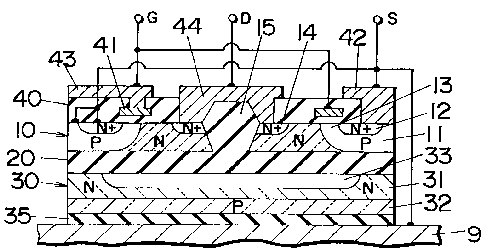
Referring to FIGS. 13 to 1 S, there is shown a solid-state relay in
accordance with a fourth embodiment of the present invention. The
relay comprises a pair of LDMOSFETs integrated into a single device of
the SOI structure composed of a N-type silicon layer 100, a buried oxide
i5 layer 200, and a silicon substrate 300. The single device is mounted on
a supporting plate 9 of an electrically conductive material with a
dielectric layer 350 interposed therebetween. A P-type well region 111
is diffused in the silicon layer 100 over the full depth thereof in such a
manner as to form therein a laterally isolated pair of first and second
2o active zones I01 and 102 of elliptical configuration. Formed
respectively around the first and second active zones 101 and 102 are N-
type first and second source regions 121 and 122 which are of closed
loop configuration and diffused in the top surface of the well region 111
to define individual sources of FETs. The first and second source
25 regions 121 and 122 also defines first and second channel 131 and 132
of closed loop within the well region between the individual source
regions and the inwardly opposed peripheries of the first and second
active zones 101 and 102. First and second N-type drain regions 141
CA 02241765 1998-06-26
- 20 -
and 142 are diffused in the top surface of silicon layer 100 respectively
within the first and second active zone 101 and 102 in a laterally spaced
relation to the well region 111 to define individual drains of FETs.
First and second insulator studs 151 and 152 are formed by the LOCOS
s technique to proj ect above the silicon layer 100 from the buried oxide
layer 200 through the centers of the first and second drain regions 141
and 142, respectively.
The top surface of the silicon layer 100 is covered with a field
oxide layer of Si02 400 having a pair of first and second gate layers 411
to and 412 of doped polysilicon, a gate electrode 431, a source electrode
421, and a drain electrode 441. The first and second gate layers 411
and 412 extend respectively over the first and second channels 131 and
132 in a spaced relation therefrom to define the individual gates of FET
and are commonly connected to the gate electrode 431. The source
15 electrode 421 penetrates through the field oxide layer 400 to reach a
portion on the silicon layer 100 bridging over the first and source regions
121 and 122 through the well region 111 formed therebetween for
interconnection of the sources of the two FETs. The first and second
drain electrode 441 and 442 penetrate through the silicon layer 100 over
2o the insulator studs 151 and 152 to contact with annuli of the first and
second drain regions 141 and 142 around the insulator studs. As shown
in FIG. 15, the gate electrode 431 is provided with a pad 531 for wiring
connection with the associated circuit element, i.e., the control unit as
shown in FIG. 1. The first and second drain electrodes 441 and 442 are
2s provided respectively with pads 541 and 542 for wiring connection to
output terminals of the relay. The source electrode 421 is provided
with a single pad 521 for wiring connection to the supporting plate 9.
The source is not necessarily connected to the supporting plate 9.
CA 02241765 1998-06-26
-21-
In the above structure, the well region 111 extends the full depth of
the silicon layer 100 to form the two isolated active zone 101 and 102 on
the buried oxide layer 200, enabling the formation of the two FETs in a
single SOI structure, in addition to reducing the drain-source capacitance
because of the reduced area of the well region 111 laterally confronting
the drain region 141, 142 and also because of the lower specific
capacitance of the buried oxide layer 200 than the silicon layer 100.
Despite that the buried oxide layer 200 has the low specific
inductive capacitance, it will give a secondary capacitance particularly
to when the source is electrically connected to the supporting plate 9. The
secondary capacitance is developed substantially in vertical paths from
the drain regions 141 and 142 to the supporting plate 9 through the
buried oxide layer 200 and is added in parallel capative connection with
the primary drain-source capacitance developed substantially in the
lateral path from the drain regions to the well region. In order to
nevertheless cancel the secondary capacitance as much as possible, the
N-type silicon substrate 300 is formed with a pair of laterally spaced
recesses 341 and 342 and is placed on the supporting plate 9 through the
dielectric layer 350.
2o Each of the recesses 341 and 342 extend the full depth of the
silicon substrate 300 and has an elliptical configuration in a horizontal
plane so as to cover a portion of the silicon layer 100 bounded by each
of the first and second source regions 121, 122 and including the first
and second drain regions 141, 142. The recesses 341 and 342 and the
2s dielectric layer 350 give individual capacitances which are added in
series capative connection with the drain-source capacitance of the
buried oxide layer for reducing the total secondary drain-source
capacitance, thereby minimizing the overall drain-source capacitance
CA 02241765 1998-06-26
- 22 -
and therefore the output capacitance.
It should be noted in this connection that the supporting plate could
be electrically isolated from the sources as well as from drain of each
FET, while assuring a greatly reduced drain-source capacitance. In
such modification, the silicon substrate would not require the recesses or
cavity, and even the dielectric layer 350 may be eliminated.
Further, it is within the concept of the present invention to combine
the specific features of the individual embodiments in order to reduce
the secondary source-drain capacitance developed through the buried
to oxide layer. Those specific features include the provision of the
insulator stud 15 through the drain region 14 (typically shown in FIG. 3),
the intervention of the dielectric layer 35 between the supporting plate 9
and the silicon substrate 30 (typically shown in FIG. 3), the provision of
cavity 33 or recess 34 (typically shown in FIGS. 3 and 10), and the
is provision of the stratums 31 and 32 of opposed type as the silicon
substrate 30 forming therebetween the P-N junction (typically shown in
FIG. 3).
CA 02241765 1998-06-26
LIST OF REFERENCE NUMERALS
1 input terminal 100 silicon layer
2 output terminal 101 drift region
3 control unit 102 drift region
4 light emitting diode 111 well region
photovoltaic cell 121 source region
6 driver 122 source region
7 frame 131 channel
8 chip (photodetector) 132 channel
9 supporting plate 141 drain region
142 drain region
silicon layer 151 insulator stud
11 well region 152 insulator stud
12 source region
13 channel 200 buried oxide layer
14 drain region
insulating stud 300 silicon substrate
16 peripheral zone 341 recess
17 separator ring 342 recess
18 land 350 dielectric layer
buried oxide layer 400 field oxide layer
411 gate layer
silicon substrate 412 gate layer
31 upper stratum
32 lower stratum 421 source electrode
33 cavity 431 gate electrode
34 recess 432 gate electrode
dielectric layer 441 drain electrode
442 drain electrode
field oxide layer
41 gate layer 521 pad for source electrode
42 source electrode 531 pad for gate electrode
43 gate electrode 541 pad for drain electrode
44 drain electrode
52 pad for source electrode
53 pad for gate electrode
54 pad for drain electrode
60 dielectric layer