Note : Les descriptions sont présentées dans la langue officielle dans laquelle elles ont été soumises.
CA 0224433~ 1998-07-29
Digital Modulator
BACKGROUND OF THE INVENTICN
(i) Field of the Invention
The present invention relates to a digital modulator for
use in a multi-level quadrature amplitude modulation (QAM)
type digital radio communication system, especially to a
digital modulator which can automatically set a modulation
parameter suitable for a change of a system transmission
parameter based on a control signal from the outside.
(ii) Description of the Related Art
A modulator whose modulation parameter is controlled at
the time of malfunction or operation is heretofore known.
For example, in a known technique, outside control data
including the modulation parameter is entered into a
modulator and controlled in a software manner. Examples of
the outside control data include control data concerning the
bit number of two orthogonal data strings or a cut-off
frequency of a waveform shaping filter. In accordance with
the control data an orthogonal data modulating section of the
modulator and the operation frequency of the waveform shaping
filter are controlled to automatically change the modulation
parameter.
In the prior art described above, the control data is
transmitted to the modulator in a software manner when the
modulation parameter is changed. Here, when power supply is
CA 0224433~ 1998-07-29
turned on in the modulator, the control data is set after
modulator operation is stabilized. In a transient state from
the turning on of the power supply till the setting of the
control data, the modulator operation becomes unstable in
some case. Furthermore, even when the control data is
entered, in a transient state in which the previous
modulation parameter is shifted to a new modulation
parameter, the modulator operation becomes unstable in some
case. In the transient states, if an output spectrum of the
modulator is spread beyond a required band which is
determined in the system, other adjoining circuits are
disadvantageously interfered with. The problem will be
described in detail with reference to the drawings.
Fig. 7 shows an RF spectrum waveform when an output
frequency of a digital modulator is converted to an RF
frequency. The spectrum waveform shown by a solid line in
Fig. 7 represents a modulation spectrum for obtaining
required characteristics. Its central frequency is
represented by fO, and its bandwidth is represented by fr.
Channels adjoining the modulation spectrum are shown by
dotted lines, and a central frequency of each of the channels
is apart by +f~ from the central frequency fO.
When malfunction occurs immediately after the power
supply turns on, and incorrect data with a double bandwidth
is set, then the bandwidth with the central frequency fO is
CA 0224433~ 1998-07-29
spread to 2fr. As a result, the modulatior spectrum becomes
an interference signal with the adjoining channels.
To solve the aforementioned problem of interference with
the adjoining channels, for example, a system is disclosed in
Japanese Patent Application Laid-open No. 77324/1989 in which
adjoining circuits are prevented from being interfered with
by lowering an output of a power amplifier. However, in the
method, since the output is lowered, an input level of a
next-stage transmission device is lowered and an apparatus
failure alarm (ALM) is therefore generated. Furthermore, in
a next-stage transmitter ALC circuit, full gain is provided.
Therefore, the interference with the other adjoining circuits
cannot be solved yet.
SUMMARY OF THE INVENTION
Wherefore, an object of the invention is to provide a
digital modulator whose modulation parameters can be
controlled in which modulation data or modulation signals are
prevented from interfering with other adjoining circuits
through control when power supply is turned on, when a system
is changed or at another setting transient time.
To attain this and other objects, the invention provides
a digital modulator which has a function of outside control
of a modulation parameter and which comprises switching means
for modulation with fixed data instead of transmission data
.. ., , . ~ , j .. , ~ ~ . , .
CA 0224433~ 1998-07-29
for a predetermined time when power supply of the digital
modulator is turned on or when a signal for the outside
control is detected.
Furthermore, the switching means is provided with a
power-on detecting circuit for detecting that the power
supply of the digital modulator is turned on, a control
signal latch circuit for detecting that a control signal for
controlling the modulation parameter is entered, an AND
circuit for detecting that an output of the power-on
detecting circuit or the control signal latch circuit is
generated, a timer circuit for delaying an output of the AND
circuit by a predetermined time and a switch for switching
the fixed data and the transmission data based on an output
of the timer circuit when the power supply is turned on or
when the modulation parameter is changed.
Another switching means is provided with a power-on
detecting circuit for detecting that the power supply of the
digital modulator is turned on, a control signal latch
circuit for detecting that a control signal for controlling
the modulation parameter is entered, an AND circuit for
detecting that an output of the power-on detecting circuit or
the control signal latch circuit is generated, a timer
circuit for delaying an output of the AND circuit by a
predetermined time and a flip-flop connected to the
transmission data for outputting a held data value just
.. . , . ~ , , ~ . . .. ...
CA 0224433~ 1998-07-29
before operation of the timer circuit based on an output of
the timer circuit when the power supply is turned on or when
the modulation parameter is changed.
Further switching means is provided with a power-on
detecting circuit for detecting that the power supply of the
digital modulator is turned on, a control signal latch
circuit for detecting that a control signal for controlling
the modulation parameter is entered, an AND circuit for
detecting that an output of the power-on detecting circuit or
the control signal latch circuit is generated and a timer
circuit for delaying an output of the AND circuit by a
predetermined time. Based on an output of the timer circuit,
a D/A converter for digital-analog converting the
transmission data is inhibited from sampling when the power
supply is turned on or when the modulation parameter is
changed.
BRIEF DESCRIPTION OF THE DRAWINGS
Fig. 1 is a block diagram of a digital modulator
according to the invention.
Fig. 2 is a time chart showing operation when power
supply is turned on in Fig. 1.
Fig. 3 is a time chart showing operation when setting is
changed in Fig. 1.
Fig. 4 is a block diagram showing a power-on detecting
CA 0224433~ 1998-07-29
circuit 23 and a control signal latch circuit 26 of Fig. 1.
Fig. 5 is a block diagram showing a second e~bodiment of
the digital modulator of the invention.
Fig. 6 is a block diagram showing a third embodiment of
the digital modulator of the invention.
Fig. 7 is an explanatory view showing an influence of an
output waveform from the digital modulator onto adjoining
channels.
DETAILED DESCRIPTION OF THE PREFERRED EMBODIMENTS
Embodiments of the invention will be described in detail
with reference to the accompanying drawings.
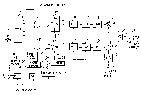
Fig. 1 is a block diagram of a digital modulator
according to the invention.
A signal entered via a data input 101 is
digital-processed by a digital signal processor (DPU) 1 to
obtain two orthogonal strings of parallel M-bit data signals.
Here, M denotes a natural number of one or more.
Subsequently, outputs are passed through a switching circuit
(SEL) 2, waveform shaping filters (FIR) 6, 6', digital-analog
converters (D/A) 7, 7', low-pass filters (LPF) 8, 8' and
multipliers (MIX) 9, 9', synthesized in a synthesizer (HYB)
12, then amplified to required levels in an amplifier (AMP)
13 and modulated with a carrier frequency f0 to obtain an
IF-band signal in an IF output 102.
CA 0224433~ 1998-07-29
The digital modulator of the invention also serves as a
22M-degree quadrature amplitude modulator. The MIX 9 and 9'
receive an output of an oscillator (fO) 11 for oscillating
the carrier frequency fO and an output of a phase shifter 10
for shifting the output phase by 90~, respectively.
Supply of a clock signal will be described. In the
invention, a reference oscillator (frequency: fg) 3 is an
original clock signal source. The frequency is divided to
frequencies (fg/(N-S)) suitable for a required system by a
frequency divider (1/(N-S)) 4 before supplied to DPU 1. The
frequency is also divided to frequencies (fg/M) by a
frequency divider (1/M) 5. The divided-frequency clocks
(fg/M) are transmitted to FIR 6, 6' and D/A 7, 7'. Since FIR
and D/A are operated through S-times over-sampling in the
22M-degree modulation system, the frequency is divided to
(S/M) times as a result. Here, S denotes a sampling number
and S=1,2,4,8,
In the digital modulator, the degree of modulation
system and the frequency of clock signal (fg/(SxN)) are
controlled in accordance with a required transmission
capacity and a working frequency. As the case may be, the
change of a roll-off ratio or the like is performed by
controlling the coefficient of the waveform shaping filter
(FIR).
Specifically, in the digital signal processor (DPU) 1
CA 0224433~ 1998-07-29
the bit number M of output strings is changed by controlling
N or S of the frequency divider (1/(N-S)) 4. Additionally,
the coefficients of the waveform shaping f_lters (FIR) 6 and
6' are controlled by controlling and changing M of the
frequency divider (1/M) 5.
Moreover, the sampling number S is controlled to reduce
a higher harmonic component output without changing the
characteristics of the low-pass filters (LPF~ 8 and 8' for
each system.
As aforementioned, the integers M, N and S are used as
the modulation parameters which are the degree of modulation
system, a data speed of modulation data and the coefficient
of the wave shaping filter.
For example, it is supposed that transmission data with
a transmission amount of 1/4 (N=4) relative to the maximum
transmission amount fg(bps) is transmitted as the
transmission data entered via the data input for one sampling
(S=1) by using the modulation system of 4 PSK (M=1). In this
case, the data of fg/4 bps and the clock signal of fg/4xl Hz
from the frequency divider 4 are transmitted to DPU 1. The
DPU1 divides fg/4 bps into two strings, which are transmitted
to SW 21 and 21', respectively. The signals are passed
through FIR 6 and D/A 7. After the waveform shaping and
analog conversion, an out-of-band higher harmonic component
is reduced in LPF 8, and the signal is modulated to the
CA 0224433~ 1998-07-29
-
carrier frequency f0. Finally, a modulated signal with the
carrier frequency f0 is outputted in the bandwidth of fg/8.
As aforementioned, in a case where the transmission
capacity of the circuit can be increased without replacing
the hardware of the modulator or in a case where a
generalized modulator is used in various systems irrespective
of the transmission capacity and the modulation system, the
parameters S, M and N are controlled in response to a control
signal (CONT) 103.
The setting is controlled by the control signal (CONT)
103 from a controller (not shown) for controlling the entire
system when the power supply is turned on and the system is
changed.
The digital modulator of the invention also has a
power-on detecting circuit (PWR ON DET) 23 for detecting that
the power supply is turned on and sending a detection signal;
an AND circuit (AND) 24 for switching data to fixed data or
data transmitted from DPU 1 after an optional time elapses
after either an output of the power-on detecting circuit 23
or the control signal 103 outputted at the time of setting
change is generatedi a timer circuit (TIMER) 25; and the
switches (SW) 21 and 21'. In the constitution, when the
power supply is turned on or the system is changed or at
another transient time, the fixed data is irst entered, and
the data is switched to the data to be transmitted after the
CA 0224433~ 1998-07-29
optionally set time elapses.
Additionally, the fixed data are set to digital bit
patterns which provide a modulation average output level at a
multi-level quadrature amplitude modulation, the output
level. As a result, the modulation output level varies only
a little when the power supply is turned on or the outside
control is performed.
Operation of the digital modulator shown in the block
diagram of Fig. 1 will be described with reference to Figs. 2
and 3.
Fig. 2 shows a waveform of each section when the power
supply is turned on.
As aforementioned, when the power supply of the digital
modulator is turned on, in a condition where no control
signal 103 is transmitted from the controller, data is
generated in DPU 1 even if no input signal is entered.
Therefore, a signal based on set conditions of the frequency
dividers 4 and 5 are transmitted through FIR 6, 6', LPF 8,
8', MIX 9, 9', HYB 12 and AMP 13 to disadvantageously
interfere with adjoining circuits.
To solve the problem, in the invention the power-on
detecting circuit 23 detects at time t0 that the power supply
is turned on, and emits a low-level (L) reset signal until
time tl when supply voltage is stably supplied to each
section. Subsequently, a high-level ~H) signal is outputted
CA 0224433~ 1998-07-29
at and after the time tl (Fig. 2(c)).
Furthermore, the control signal 103 is outputted to send
system setting serial data at a certain setting time t2(Fig.
2(d)). Here, a time (power-on time) from time tO to time t2
is defined as a time Tp. In Fig. 2, the system setting data
is sent for a setting time Ts from time t2 until t3, and the
serial data is of a high level (H) at another time.
The signal is transmitted to the control signal latch
circuit 26, and a low-level (L) voltage at the time of
control or a high-level (H) voltage at the time of no control
is generated in the output of the AND circuit 24 (Fig. 2(e)).
The output of the AND circuit 24 is transmitted to the timer
circuit 25, and reaches a high level (H) after time t3
elapses after the power supply is turned on. After a
switching time Tc elapses, a high-level (H) output is emitted
from the timer circuit 25 at time t4, and SW 21 is switched
(Fig. 2(f)).
In Fig.2(g), the fixed data is transmitted for a time
Tdl as below.
Tdl=Ts+Tc+Tp (1)
The time of system setting change will be similarly
described with reference to Fig. 3. The setting time Ts of
the system setting serial data for which the setting data is
transmitted via the control signal 103 to the switching
circuit 2 is equal to the time (t3-t2) of Fig. 2 (Fig. 3(b)).
CA 0224433~ 1998-07-29
Additionally, system setting start time is represented
by t5. In the control signal latch circuit 26, the system
setting data is entered and latched, and a low-level output
is emitted for the time (t3-t2). As a result, the output of
the AND circuit 24 is of a low level for the time Ts from t5
until t6, and reaches a high level afterwards (Fig. 3(c)).
Therefore, the output of the timer circuit 25 reaches a high
level at time t7 after the switching time Tc elapses, so that
SW 21 is switched.
By setting the time Tc for switching the fixed data to
the transmission data in the timer circuit 25 to
Tc>time(t2-tl) in consideration of the time for turning on
the power supply, the modulated output can be prevented from
being spread at the setting transient time.
In Fig.3(e), the fixed data is transmitted for a time
Td2 as bellow.
Td2=Ts+Tc (2)
Constitutions of the power-on detecting circuit 23 and
the control signal latch circuit 26 constituting the
switching circuit 2 of Fig. 1 will be described with
reference to Fig. 9.
The power-on detecting circuit 23 is provided with, for
example, a capacitor (C) 233, a resistance (R) 232 and a
buffer IC ~IC) 231. When the power supply is turned on, an
output of the buffer IC 231 is adjusted by time constants of
CA 0224433~ 1998-07-29
C and R in the circuit in such a manner that the output
reaches a high level after time tl elapses. An adjustment is
made in such a manner that a voltage of power supply input
'PS' is raised via a CR time constant circuit to exceed a
threshold voltage of the buffer IC 231 at the time tl.
The control signal latch circuit 26 will now be
described.
The control signal 103 is transmitted to the control
signal latch circuit. The control signal 103 ls constituted
of control data and clock signals. The number of the clock
signals is counted by a counter 261, and an output TC of the
counter 261 is transmitted to an AND circuit 262 together
with the system setting data. Furthermore, the output TC of
the counter 261 is set in such a manner that a high-level
output is emitted after a time required for system setting,
corresponding to (t3-t2), elapses after the input of the
reset signal.
When the system setting starts, the control data once
reaches a low level.
~hen the control data is entered, the output of the AND
circuit 262 in the control signal latch circuit 26 reaches a
low level to turn on the counter 261. After the counter 261
counts the number of clock signals for the time (t3-t2) based
on clock input, the counter emits a high-level output. At
this time, the control signal data has been set and has
CA 0224433~ 1998-07-29
14
reached a high level.
As a result, the output of the control signal latch
circuit 26 is of a low level only for the system setting time
(t3-t2), and transmitted to the AND circuit 24 shown in the
switching circuit 2 together with the output of the power-on
detecting circuit 23. The output reaches a high level after
time t4 elapses after the output is transmitted to the timer
circuit 25.
A second embodiment of the invention will be described
with reference to the drawings. In the first embodiment
shown in Fig. 1, the switch 21 is used, but the invention is
not limited thereto. For example, as shown in Fig. 5,
flip-flop circuits 27 and 27' can be used instead of the
switches 21 and 21'. Specifically, while the timer circuit
25 is operated, the same effect as that of the first
embodiment can be obtained by holding data at a data value
just before the timer circuit 25 is operated.
Furthermore, in a method according to a third
embodiment, as shown in Fig. 6, the switch 21 is not used.
The output of the timer circuit 25 is transmitted to reset
terminals of D/A 7 and 7', and the sampling of D/A 7, 7' is
stopped while the output of the timer circuit 25 is in a low
level. Thereby, the same effect as that of the first
embodiment can be obtained.
In the digital modulator of the invention, the power-on
CA 0224433~ 1998-07-29
detecting means is provided for detecting that the power
supply is turned on, and the transmission data is set to a
fixed value for the time required for completing the system
constitution setting. Therefore, by setting the fixed data
for the optional time after the power supply turns on and by
emitting carrier outputs until the required system
constitution setting is completed, the interference with the
other adjoining circuits is effectively inhibited.
Furthermore, the digital modu]ator of the invention has
the detector for detecting the presence of the control for
changing the system after the power supply turns on.
Therefore, since the fixed data is set for the time from the
setting start until the setting completion with a
predetermined time added thereto and carrier outputs are
emitted until the required system constitution setting is
completed, the interference with the other adjoining circuits
can be effectively suppressed even when the system is
changed.
Moreover, in the invention, in order to make the carrier
output level at the setting transient time equal to that at
the usual time, the fixed data can be defined. Therefore,
since a method of lowering the output of the power amplifier
is not used different from the conventional system, the alarm
about level decrease of the transmission device is prevented
from being generated by output decrease. Alternatively, the
CA 02244335 1998-07-29
interference with other adjoining circuits can be effectively
prevented from being caused by the full gain of the
transmitter ALC circuit.