Note : Les descriptions sont présentées dans la langue officielle dans laquelle elles ont été soumises.
CA 0224~072 1998-08-17
ONE BIT DIGITAL QUADRATURE VECTOR MODULATOR
FIELD OF THE IN~-ENTION
The present invention relates to electronic signal
processing and, in part:icular, to a digital quadrature vector
modulator using a single bit delta-sigma modulation and a
method for generating signals using the same.
BACKGROUND OF THE INVENTION
The invention applies to the fields of electrical
engineering, electronics, communications engineering and
signal processing. The quadrature modulation technique is
applicable to virtually all quadrature modulation schemes,
which include for example, Quadrature Amplitude Modulation
(QAM), Quadrature Phase Shift Keying (QPSK), Quadrature
Quadrature Amplitude Modulation (Q2AM), Orthogonal Frequency
Division Modulation (OFDM) and many others s-hemes.
Analog Quadrature Vector Modulation (AQVM)
Quadrature ~Jector Modulation using analog techniques is
currently in wide use in communications and in many other
fields which require signal processing. Commercial AQVMs,
such as that illustrated in Figure 1 are available from
suppliers such as Mini-Circuits Division of Scientific
Components, Hewlett-Packard Co., Wathins Johnson Co., Analog
Devices, Inc. and many others. These devices are useful for
general signal processing applications and are often used to
implement single side-band (SSB) radio frequency signal
modulation. Typ-cal input spectrum 20 and output spectrum 22
for SSB AQVMs are shown in Figure 2. The mu_tiplier functions
CA 0224~072 1998-08-17
in AQVMs are often realized using di.ode mixers, fieid effect
transistor (FET) based mixers, four quadrant: multipliers such
as Gilbert cells, or other analog multipliccltion techniques.
The quadrature components for the ir.put signal may be created
using hybrid baluns if the bandwidth of the input signal is
limited. In communicat:ions systems the input signals are
often digital baseband signals, the quadrature components
being generated digita]ly and subsequently converted to
baseband analog signals before they are input to the AQVM.
In general a signal 24, fB, to be input to an AVQM is
split (by e.g. a splitter 2 shown in Figure 1) into in-phase
and quadrature componerLts~ IB and QB :respectively. The
quadrature input signals may be generated using analog
techniques, but, as noted above, are usually generated
digitally and converted into analog prior to input to the
vector modulator. AS shown in Figure 1, an ~nalog modulating
signal, often ge~erated by a local oscillator (LO) 4 is also
split by a split er 6 into quadrature components, ILO and QLO.
The quadrature cl~mponents and the in--phase components are
multiplied by muLtipliers 8 and summed by a summer 10 to
produce IB*ILo + Q~*QLO. The resulting output creates upper and
lower sideband products 28 and 30 centred about the local
oscillator frequency 26 as shown in Figure 2 The lower
sideband 28 is composed of in-phase I and Q products while the
upper sideband 30 is composed of proclucts of opposite phase.
If the amplitude and phase matching of the analog modulators
is very good, the upper sideband (USE,) signa'. amplitude will
be very small compared to the in-phase lower sideband (LSB)
signal amplitude. The ratio 32 of the amplitude of the in-
phase sideband to the out-of-phase sideband products is often
CA 0224~072 1998-08-17
referred to as the ima~e rejection, image suppression or
sideband suppression. The cancelled sideband is often
referred to as the imaqe.
In a similar fashion an upper sideband may be obtained by
interchanging the ILO and QLO products to obtain I3*QL" + Q~*ILo.
It is desirable in many communications applications to
conserve bandwidth by using only a single sideband of the
modulation products. However, because the requency offset of
the image (i.e. the unwanted sideban~) from the desired
sideband signal, fLO-(fLO-fB), is often very small compared to
the local oscillator frequency, fLO, it may ~e very difficult
or impossible tc remove the image frequency by means of a
filter. For this reasc,n the image rejection performance (i.e.
the unwanted sideband suppression) of the AQVM is of critical
importance to the overall performance of the modulation
technique and can be a fundamental limiting factor in the use
of the technique. The image rejection of AQVMs varies
depending upon t.~e application, but is typic~lly between 15
and 45 dB. Reje-tion above 30 dB of en requires special
manual tuning an~ often varies with 1emperat~re and frequency.
For these reasons AQVMs can be costly to implement in large
volume applications.
The Shannon-Hartley theorem ~Modern Ouadrature Amplitude
Modulation, Webb and Hanzo, IEEE Press 1995, p. 39) states
that the capacity and maximum transmission rates of a
communications channel are limited bv the available carrier to
noise ratio. The image level from digital quadrature
modulators presents noise like interference lo the modulation
scheme and hence poses a fundamental limit to the level of
CA 0224~072 1998-08-17
modulation and transmission rates which can be achieved using
these analog modulator,.
Digital Quadra ure Vector Modulatior ~DQVM)
As taught by the Nyquist Sampling Theorem, it has long
been understood that communications signals may be fully
represented by their dlgital equivalents (Certain Factors
Affecti~g Telegraph Speed, H. Nyquis~, Bell System Tech
Journal, Apr 1928, pp. 617). It is also widely known that
quadrature vectcr modulation can be accomplished using digital
techniques. Dicital signals, however suffer from noise caused
by the quantization process. The signal-to-noise ratio (S/N)
of a signal quantized t:o n bits and having an equal
probability of existincr at each of the 2n levels, is given by
the relationshi~ 2010g~n2-l) dB and -Lncrease., by 6 d3 per bit
(Introduction to Communicaticn Systems, F.G. Stremmler,
Addison Wesley 1977 pp. 455).
Conventional digital modulators can be implemented in
many forms. For example commercially available dedicated
hardware multipliers, for instance, from Analog Devices Inc.,
can be used. De~icated signal processing components such as
the Texas Instrurnents TMS320 family of digital signal
processor integr~ted circuits may also be used. It is also
possible to implement a digital modulator in software using
general purpose -omputers such as the Intel x86 family of
processors. ConJentional Digital Signal Processors (DSP) can
achieve excellen_ image rejection due to the level of phase
and amplitude ma~ching which can be rnaintained in the digital
process.
CA 0224~072 1998-08-17
Conventional DSP t:echniques quantize bcth the baseband
and the modulating signals to a sufficient number of bits to
keep the noise to acceptable levels for the system
application. Mcdern communications systems often require 10
bit quantization or higher.
Conventional DSP requires a number of multi-bit digital
multiplications to be executed to conplete the modulation
function. These multiplications must be executed in real
time. The circuits required to exec-lte such multiplications
utilize a large number of digital gates that consume a
relatively large amount of power, and are li~ited in their
maximum clock rates due to the size and complexity of the
digital computations required. Because of the size of the
integrated circuits involved, multi-bit multiplication
circuits are rel~tively expensive and operate at slower clock
speed than singl- bit digital circuils using the same
technology. The use of multi-bit digital quadrature vector
modulation is therefore often limited in its applicability to
high speed communications systems because of cost, complexity,
size, power requirements, and performance liinitations of the
circuits required by conventional techniques.
Delta Sigma (~) Modulation
Over the past twenty years a number of authors have
described ~ modulators for use as Digital-to-Analog
Converters (DACs,. See for example Oversamp_ing Delta-Sigma
Data Converters, Candy and Temes, IEEE Press (1992). Delta
Sigma modulation is a method of achieving high signal-to-noise
ratios over limited bandwidths using single bit signals
modified by feedback. ~ modulators require high sampliing
CA 0224~072 1998-08-17
rates relative to the applied signal To date ~ modulators
have not been widely used in communications applications
because of the ~eed for very high clock rates to support the
required samplirg rates. This is changing, however, as
semiconductor feature sizes allow faster and faster clock
rates. It is t~erefore now possible to use ~ modulators in
communications applicat:ions, and these are now commercially
available as, fcr example the National Semiconductor ADC16701.
SUMM~iRY OF THE I ~ ENTIC)N
It is an object of the present invention to provide a
means for performing quadrature vector modulation digitally
using circuits which are more readily adaptable to high volume
manufacturing than conventional multi-bit digital modulation,
and for achieving high suppression of the unwanted sideband in
the single sideband upconversion of the DQVM.
The One Bit Digital Quadrature Vector M~dulator (DQVM)
and a method of ~enerating single sideband output signals of
the present invention are useful for a wide range of radio
frequency, signal processing and wireless applications. The
DQVM simplifies the necessary digital multiplication by using
noise shaped one bit versions of both the ba~eband IB and QB
signals to be modulated and the ILO and QLO mcdulating signals.
The one bit DQVM enables a much faster digital implementation
of the digital quadrature vector modulation function than can
be achieved with conventional multi-bit digi al techniques.
Digital vector modulators are an imp.-ovement over conventional
analog vector modulators as they are not subject to the
amplitude and phase matching problems inherent in analog
vector modulator,. Furthermore, the single sideband
CA 0224~072 1998-08-17
upconversion of the DQVM of the present invention achieves
high suppressior of the unwanted sideband by applying an
offset to one of the input samples.
In accordance with one aspect of the present invention,
there is provided a met.hod for producing a single bit stream
using digital quadrature vector modulation. The method starts
by receiving multi-bit digital in-phase and quadrature input
signals at a baseband sample rate. An offset is implemented
on one of the input signals at the baseband sample rate. The
offset input signal and. the other on- of the input signals are
modulated into single bit delta-sigma (~) c~ded bitstreams at
a modulator sampling rate which is faster thLn the baseband
sample rate. Orthogonal clock signa:ls are created at a
sampling rate equal to the modulator sampling rate and an
effective frequency equal to one hal,- of the modulator
sampling rate. Then, the ~ coded bitstreams are multiplied
with the orthogonal clock signals so as to create two product
single bit streams at the modulator sampling rate. The two
product single bLt streLms are alternately combined into'a
interleaved sing~Le bit stream so that the interleaved single
bit stream is clocked at a rate twice the modulator sampling
rate.
In accordance with another aspect of the present
invention, there is provided a Digital Quadrature Vector
Modulator (DQVM) system comprising an offset implementing unit
for implementing an offset on one of multi-bi.t digital in-
phase and quadrat:ure input signals received at a baseband
sample rate; a fi,rst one bit delta-sigma (~) modulator for
receiving and modulating the offset input signal at a
modulator samplirg rate which is faster than the baseband
, ~
CA 0224~072 1998-08-17
sample rate and outputting a single bit a~ coded bitstream of
the offset input signal; a second one bit ~ modulator for
receiving and mo~ulatin.g at the modulator sampling rate a non-
offset input signal which is the other one of the input
signals and outputting a single bit ~ code~ bitstream of the
non-offset input signal; means for c:reating ~rthogonal clock
signals at a sam~ling rate equal to ~he modulator sampling
rate and an effe~tive frequency equa:L to one half of the
modulator sampli~g rate; a first multiplier for multiplying
the ~ coded bitstream of the offset input signal with one of
the orthogonal clock signals so as to create a first product
single bit strearn based on the offset input ignal; a second
multiplier for m1ltiplying the ~ co(ied bits_ream of the non-
offset input wit:a the other one of the orthogonal clock
signals so as to create a second product single bit stream
based on the non-offset input signal and a multiplexer for
alternately combining the first and second product single bit
streams into a interleaved single bit stream so that the
interleaved singLe bit stream is clocked at a rate twice the
modulator sampling rate.
Other advantages objects and features of the present
invention will be readily apparent to those skilled in the art
from a review of the following detai]ed descriptions of the
preferred embodiT~ent in conjunction with the accompanying
drawing and cla iT-lS.
BRIEF DESCRIPTION OF TH~ DRAWINGS
The embodiments of the invention will now be described
with reference tc~ the accompanying drawings in which:
Figure 1 is an ana:log quadrature vector modulator;
CA 0224~072 1998-08-17
Figure 2 is a quadrature modulator input and output
spectra;
Figure 3 is a one bit digital quadrature vector modulator
input and output spectra;
Figure 4 ic a functional block diagram of an embodiment
of a one bit Digital Quadrature Vector Modulator (DQVM) in
accordance with the present inventicn;
Figure 5 is a chart showing the relati-~e timing of select
waveforms in the one bit DQVM;
Figure 6 is an example of a preferred embodiment of the
one bit DQVM;
Figure 6A is a chart showing details o the relative
timing of select waveforms in the one bit DQV~ of Figure 6;
Figure 7 is a diagram showing an analog representation of
the Q baseband signal; and
Figure 8 is an example of a sim~le linear interpolator
which may be implemented in the embodiment of the one bit DQVM
shown in Figure 4.
DESCRIPTION OF T~E PREFERRED EMBODIM~'NTS
With refere~ce to Figures 4 to 1" the embodiments will
describe a lower side-band realization. Realization of the
upper sideband version of the invent:ion is a straight forward
adaptation of the process described herein.
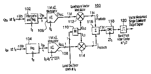
Figure 4 shows a block diagram of a Dig:ital Quadrature
Vector Modulator (DQVM) 100. The DQ~ 100 generally consists
of sections to implement the following functions: (l) A
section to receive two (2) multi-bit (where n is the number of
bits) digital quadrature input signa s I~n and Q~n and where the
signal sample rale is f~ samples per second; (2) a section or
CA 0224~072 1998-08-17
method to imple~ent a clelay on the Qan data, and to output the
delayed data, Q~n: the delay is equi-valent t~ one period of
the Digital Analog Converter (DAC) clock, T~C = 1!2fS; (3) a
section or methcd to modulate the multi-bit quadrature signals
IBn and Q' Bn into single bit ~ coded bitstreams IB~ and Q' B~ at
a modulator samFling rate f5, fs = fB * 2 * OSR, where OSR is
the Over Samplirg Ratio (OSR); (4) a section or method to
create orthogonal ILO and QLO clock signals, which will play the
function of local oscillators, and where the orthogonal clock
signals are represented by single bit words at a sampling rate
equal to the sampling rate of the ~ bitstreams; (5) a section
or method to multiply the IB~ and Q'~"~ bitstreams with the ILO
and QLO clocks w~ere the high clock signal will not change the
input data bit and wher-e a low c:lock signal will invert the
input data bit, thus creating the two product single bit
streams I3~*I10 and Q'3~*QLO at the fLC sampling rate fSi (6) a
section or metho~ to register the two product bitstreams and
to alternately combine the two bitst:reams in~o a single
interleaved bitstream, I~*ILo+Q~ *QLcl~ where the resulting
bitstream is clo-ked at 2fs, twice the rate of the local
oscillator clock sampling rate; (7) a section or method to
convert the single bit stream into an analog signal with two
well defined output voltages whereby one ana:log voltage
represents the digital high bit and a second analog voltage
represents the digital low bit; (8) a sectiorL or method to
band pass filter the resulting single sideband analog signal
whereby the analog filter must have sufficiellt rejection to
reject the noise create~ from the ~ modulat:ion to the level
required for the particular applicat on.
CA 0224~072 1998-08-17
Section (2) compr_ses an interpolator a.nd register 102
which receives the Q~n signal and a f~ clock. An interpolator
and a register may be E)rovided separately. The I~n signal is
input to a register 104 which also receives a f3 clock.
Section ~3) comprises 1 bit ~ modulatcrs 106, 108. Each
modulator 106, 108 receives the Q'Bn and IBn, respectively, and
a fs clock.
Section (4) compri.ses a splitter 110 which receives a
local oscillator clock at fs and outputs the QLO and ILO clock
signals, which are input to multiplexers 112, 114 of section
(5), respectively.
Section (6) comprises a summer 116, and section (7)
comprises a Digital-Analog Converter (DAC) 118 which receives
a 2fS clock. Section (8) comprises a band pass filter 120
whose centre is at fS/2, or at odd multiples of fS/2.
The circuit functions just described can be implemented
in a wide range ~f technologies including both discrete and
integrated embodiments of the circui_s and with a wide range
of variants on the methods to implement each functional block.
Figure 3 shows the input spectrum 40 and the output
spectrum 42 of a typical digital Quadrature Modulator using
single bit delta sigma modulators. The input I or Q baseband
n bit data 44, a~ frequency fdata, is represented in the
spectrum 40. The baseband signal 44 has whi-_e noise 46 at a
level which is related to the number of bits of resolution in
the samples, n, and the ratio of the baseband data sampling
frequency 48, f ~ .
The n bit baseband data 44 at fE is then modulated by
delta sigma data converter running at: a samp:Ling rate 50 Of fs.
CA 0224~072 1998-08-17
The output of the I anc Q modulators is a s ngle bit each at
the fs rate.
The noise out of the modulators is shaped such that the
noise near the data is low and higher in fre~uency the noise
increases. This is reFresented in tne spectrum 42 by the
lines marked Baseband ~ata 44 and the Baseband Delta Sigma
Sampling Noise 52.
A similar s?ectrum exists at the output of the I and Q
modulators where each output represents the I and Q baseband
data respectivel~.
The two modllator outputs are passed through the output
mixing and combi~ing stages and are combined into a single
output at the 2f~ rate. The resultirg outpu. spectra is
centered at odd multiples of fS/2 a wanted sideband 54 appears
in this example at fs/2 - fdata a suppressed carrier is at the
center of the band and an unwanted upper sideband is
suppressed at fs/2 + fdata. The dotted line 5f~ represents a
typical bandpass filter passband for selecting the first alias
output of the SS}3 output. The multiplexer operates at a mux
clock frequency 58 2fS.
Normally the IBn and QBn signals shown in Figure 4 exist
as multi-bit dig:tal sequences. A preferred method of
producing single bit baseband signals for quadrature
modulation uses a data interpolator t:o produce a Q Bnsignal
and then uses digital delta-sigma (A~:) modulation to convert
the multi-bit I3n and Q Bnsignals into single bit bitstreams
IB~r and Q B~. The noise shaped single bit signals IB~j~ and Q
are multiplied by single bit ILO and QLO signals and then
combined. The resulting single bit single side band (SSB) ~
data stream represents the bandpass spectrum of the quadrature
CA 0224~072 1998-08-17
modulated baseba~d signals (to the precision of the
quantization) with no amplitude or phase mis~natch between the
I and Q components of the signal. T~e analog RF spectrum is
easily generated from the SSB a~ bit,tream by means of a
conventional 1 bit Digital-to-Analog Convert~r (DAC) and Band
Pass Filter ~BPF). The analog RF spectrum can be demodulated
by any standard .~F receiver.
The present invention, shown in block diagram form in
Figure 4, makes ~se of a signal interpolator and two single
bit ~ modulators to create single b:it, noise shaped, digital
baseband representations of multi-bi~ quadra-ure input
signals. The us- of single bit, noise shaped, digital
baseband signals enables a digital modulation scheme which is
far simpler and requires fewer functional parts than multi-bit
modulation methods. An apparatus constructed in accordance
with the invention can also run at h-Lgher clock rates than
multi-bit modula~ion apparatus. One bit noise shaped single
bit ~ oversamplLng in accordance with the invention is
preferred over conventi~nal single b-t pulse code modulation
(PCM) as they can achieve much higher Signal to Noise ratios
for a given sampLing rate. Single b t digit~ll quadrature
modulation perfo~ms in a similar fashiorl to rnulti-bit digital
quadrature modulation in terms of image rejection, phase and
amplitude matching. Hence image rejection is superior to
analog modulators.
Using modern semiconductor processes, s ngle bit digital
vector modulation can now be implemented at sufficiently high
speeds to replace analog vector modu,.ators for a wide number
of signal processing and communications applications.
CA 0224~072 1998-08-17
After upconversion to a single sideband, the one bit
digital a~ bitstream is converted to analog using a
conventional 1 bit DAC. The resulting analog signal has a
noise shaped spe~trum and is filtered using a conventional
band pass filter.
Quadrature bitstreams which have been modulated by an ILO
and QLO clocks must be combined to generate the desired SSB
signal. Normally the digital samples from the I and Q
bitstreams are combined by summing the signa:Ls. If the LO
clock phase advances by less than 90" per data sample the
required digital summation is complex or complicated, i.e.
involves multi-bit numbers, is usual:y slow and is generally
not practical fo-- high speed communications applications.
However, if the ~,O clocks advance by exactly 90~ per data
sample, that is the data is multiplied by clock signals at
only the four distinct phases of 0, '30, 180 and 270 degrees,
then every second LO clock sample has an ampLitude of exactly
zero. Since the LO clocks are offset: by 90~ no physical
summation is required as one or the other clock signal is
always zero. Hence, when using the 4 phase clock approach,
the modulated quadrature bitstreams may be combined by a
simple multiplexer technique. The product of- the LO clock and
the input signal which occurs when the LO Clock is zero is
hence, never used, and need not physically exist. Hence the
LO clocks may run in quadrature and only sample the input
waveforms at the two phases of 0~ and 180~ for the cosine clock
and 90~ and 270~ for the sine clock.
The resulting summation is achieved by multiplexing
between the two modulated bitstreams at twice the LO clock
rate.
14
CA 0224~072 1998-08-17
Since the actual samples used by the interleaving process
are offset by the multlplexer clock period, i.e. 1/(2xfs),
then the basebard input Q data must be sampled at 1/(2fs)
seconds later than the I data. This of~set in baseband
sampling by the small amount of the multiplexer clock rate
will lead to perfect image cancellation. Should the offset
not be applied to the baseband sampling the DQVM SSB
modulation will still function, but with some degradation in
the image rejection. If the oversampling rate are high
enough, image rejection will still be superior to most
(analog) AQVMs regardless of whether or not the offset is
applied, but the baseband offset is necessary for many high
resolution appli_ations.
It is therefore preferred that he data supplied to the
DQVM be offset sampled as described above, and passed to the
DQVM synchronously at the common sample rate. Should the I
and Q input data be sampled at the same time without offsets,
and for practical reasons must be passed to the DQVM as such,
and should the irnage rejection of the non-of-set data not be
sufficient for the application, then an interpolation circuit
is required on one of the input samp]es, e.g the Q data, to
interpolate between the sample points to determine the value
of the Q sample at the offset time. Many types of signal
interpolators ex~st which may be used for this purpose and
include such tec~miques as look up tables, or techniques
similar to those described by Ritchie et al. (Interpolative
Dlgital to ~n~log Converters Ritchie, Candy and Ninke, IEEE
Transactions on Communications, Vol. COM-22 p. 1797-1806,
Nov. 1974). The accuracy of the interpolation will determine
the ultimate image rejection achievakle. For many
CA 0224~072 1998-08-17
applications simple linear interpolation between the sample
points would be sufficient to improve image rejection to the
desired level fcr the application.
An example of a hardware method to achieve the simple
linear interpolation may be described as follows.
Figure 7 shows an analog representation 160 of the QB
input baseband waveform superimposed on the actual digital
samples for illustration purposes. If it is assumed in this
example that the Q~ waveform needs to be corrected using the
interpolator then the sequence of n-bit qua~rature baseband
samples QBni may ~e represented as fo_low:
QBni = QBnl / QBn2 / QBn3 / ~ - - -
where i is an in-reasing integer and the i subscript
represents samples taken at the baseband sample rate fB
(samples/seconds) and are hence separat.ed in time by 1/fB
(seconds/sample).
If the baseband samples are later delta sigma modulated
to create 1 bit versions of the signal at the sample rate fs~
and then the samples are interleaved and output as the SSB
signal at the 2f rate then the interpolaticn required is the
value of QB signal at 1/2fs seconds after the actual samples
QBni -
The new sequence will generate a new series of numbers
Q Bni-
Figure 8 shows an example of a simple li.near interpolator
170. An n-bit quadrature signal QB iS input to a register 172
which registers t.he input signal at a sampling rate of fB. The
output of the register 172 is input via a del.ay unit 174 to a
plus terminal of an adder 176 and directly to a minus
terminal of the adder 176. Thus the output of the adder 176
16
CA 0224~072 1998-08-17
represents a slope of the neighbouring two quadrature signals,
e.g. QBn1 and Qr~n2. The output of the adder 176 is multiplied by
fB/2f5 by a gain block 178 to produce an offset value signal.
The offset value signal is then added to the original output
of the register 172 by an adder 180 so as tc, output a offset
n-bit Q' B signal.
The simple linear interpolator ~70 shown in Figure 8
realizes the interpolation at 1/2fS Later by effectively
calculating the slope (i.e. the difference) between any two
points QBni and Qgni~1, and multiplying the slope by a gain
factor equal to the ratio of the desired delay to the baseband
sample rate, i.e. Q' Bni = fg/ (2fs) * (QBr~+l ~ QBnl )
The resulting output sequence will have an improved image
suppression over a sequence with no interpolation. The image
suppression is related to the oversampling ratio and the
number of bits used to represent the interpolation. Either one
can be increased to realize the necessary image suppression.
The choice of which method or combinat_on of methods to use
will be dependant upon the practical constraints of the
problem such as power consumption, maximum clock speeds, cost
etc.
The following describes a simple embodiment of the
invention which rnay easily be realized in an integrated
circuit.
Figure 6 shows the input multi-bit bitstream IBn and QBn
where both signals represent samples of the baseband data at
fB. Due to the fact that the digital quadrature signals will
be interleaved at the output of the DQVM at t:he 2f5rate, it is
necessary that the Q'Bn signal be sampled at C.5Ts(Ts=1/2fs )
after the IB signal. The preferred embodiment is to register
CA 0224~072 1998-08-17
the IE3n and Q~3n samples simultaneously into the DQVM, but to
offset the effective sampling time cf 0~5Ts in software or
hardware prior to input to the DQVM. Simultaneous clocking of
the two input signals greatly simplifies the clock generator
circuitry of the DQVM. An error in the samFling time will
result in a phase error in the I and Q signals and will result
in reduced image suppression as is seen in analog vector
modulators. The method shown interpolates the QBn signal to
create the needed Q~3n signal in hardware, i.,-. a register and
interpolator 102. A method is provi~ed to modulate the two
bitstreams using any single bit delt~ sigma modulation
technique 106, 108. The resulting OltpUt bltstreams at fs are
input into one terminal of exclusive OR (XOR) gates 152, 154,
or functional equivalent, and where he other terminal is
clocked by a one bit clock fLO, also at fs. High bits from the
fLOhave the effect in the XOR gate 152, 154 of passing the ~
data through unmodified, i.e. with a gain of unity. Low bits
from the fLOhave the effect in the XOR gate of inverting the
~ data, ie a gain of -1. The single bit synchronous outputs
of the two XOR gates 152, 154 are input to a multiplexer 156
which latches the two bitstreams and alternately clocks out
the I and Q bit streams at a multiplexer clock of 2fS This is
equivalent to inserting zeros between each sample for the I
and Q bit streams and results in each bit stream being
multiplied by repeating sequences of 1 0 -1 0 at 2fS. Since
the repeating sequence is four cycles the resulting SSB data
will be created at fs/2, and will have aliases at nfS/2 where n
is an odd integer. The output of the combined ~ bitstream
will be a SSB waveform with a noise null at the centre of the
SSB spectrum. T~e combined ~ bitstream may be converted to
18
CA 0224~072 1998-08-17
an analog waveform with either a zero order sample and hold or
~irac function type DAC 118. The zero order sample and hold
version will hav-e a sinx/x rolloff with the first null at 2fS
It is important that the output of the DAC have symmetrical
rise and fall times to avoid degrading the Q~ spectrum noise
null. Depending upon the application and the selection of IF
output frequency from one of the abcve aliases, the signal
will have a certain amount of sinx/x shaping on the output
spectrum. A slightly more complex version of the DAC may be
realized using a Dirac impulse function DAC to reduce sinx/x
rolloff. Finally a simple band pass filter 120 is required to
remove the unwanted a~ aliases and ~, noise from the complex
modulated output signal. The bandwidth, order and ultimate
rejection requirements of the Band Pass Filter are dictated by
the specific requirements of the mod-~lation scheme being used
and the type of ~ modulation used.
Figure 5 re?resents the relative tlming of select
waveforms in the one bit DQVM. Line 130 shows the baseband
sampling rate of the input data, fB c:lock; li.ne 131 shows the
modulator sampling rate at fs; lines 132 and 133 show the
orthogonal clock signals ILO and QLO/ respectively, which will
be multiplied wi,h the IBA~ and Q'B~ bitstreams by the XORs.
Line 134 shows the multiplexer clock rate 2f~. The last row
135 shows the output data sequence.
Figure 6A represents more details of the relative timing
of select waveforms in the one bit DQVM. The baseband
sampling rate of the input data, fB, is slow (line 136)
relative to all c>ther waveforms. Bot:h I and Q input data use
the same sampling rate at the same phase.
CA 0224~072 1998-08-17
The samplirg rate of the I and Q delta sigma modulators,
fg, is a high integer multiple of the baseband sampling rate
(line 137).
The I and ~ delta sigma modulator output data are shown
as DSI (line 138) and DSQ (line 139) respectively.
The ILO (cosine LO) and the QLO sine LO) operate at a
frequency of fs/7/ that is one half of the delta sigma clock
(lines 140, 141). Normally the LO signals would have four
levels, for example 1, 0 -1, 0 for the cosine LO, and 0,1,0,-1
for the sine LO, however since the i~terleaved I and Q later
on does not require the 0 products, the ILO and QLO appear
identical. In fact we use the DSI and the DSQ data in a
fashion equivalent to the output which four level quadrature
LO signals would produce.
The product of the DSI waveform and the ILO is shown by I*
(line 142) and similarly the DSQ*QLO product is represented by
the Q* waveform (line 143). The negative products are
achieved by inverting the data when ~he LOs are in a low
state.
Finally the I* and Q* waveforms are summed in an
interleaved fashion at the 2fs rate (line 144) to produce the
single sideband output data stream. The OUTPUT waveform when
viewed in the frequency domain, and after bandpass filtering
produces the desired high resolution SSB spectra from the DQVM
(line 145).
The one bit technique enables a much faster digital
implementation of the digital quadrature vect:or modulation
function than that which can be achieved with conventional
multi-bit digita. techniques. The digital vector modulator is
an improvement over conventional analog vector modulators as
CA 0224~072 1998-08-17
it does not suffer from amplitude and phase matching problems
seen in analog vector modulators. The ~QVM is also an
improvement over single bit digital modulators which suffer
from reduced image suppression due to sample timing errors.
Numerous modifications, variations and adaptations may be
made to the particular embodiments of the invention described
above without departing from the scope of the invention, which
is defined in the claims. For example, in the above preferred
embodiments, the quadrature signal Q~ is delayed, but the in-
phase signal IB may be offset rather than Q~ Also, the
present inventio~ may be implemented by a computer processor
or similar device programmed to execute the method steps
described above, or may be executed by an electronic system
which is provided with means for executing these steps.