Note : Les descriptions sont présentées dans la langue officielle dans laquelle elles ont été soumises.
CA 02246838 1998-12-03
DUAL-BEAM GROUND CONTACTS HAVING A REALIGNMENT TWIST
FOR GANG INSERTION INTO AN INSULATOR HOUSING
Background
The present invention relates generally to the art of electrical connectors
and, more
particularly, to a "card edge" electrical connector for a printed circuit
board. In even
greater particularity, the present invention relates to dual-beam ground
contacts having a
realignment twist for gang insertion into the insulator housing of a card edge
electrical
connector.
Historically, prior art electrical connectors have been assembled by very
tightly
press fitting or molding contacts into receiving blocks of insulative material
which form
structural members to support the contacts and hold them rigidly within the
insulative
body. The prior art connector having contacts rigidly fixed within the
insulator are then
mounted by bolting the insulator to a pair of spaced parallel rails, or by
dropping the
contact tails into holes in a mounting substrate and soldering them in place.
The prior art
techniques for assembly of the aforesaid connectors are relatively slow
because of the time
required to rigidly mount each individual contact into its receiving sleeve
within the
insulator. Certain prior art connectors have overcome this problem by
providing for
simultaneous insertion of rows of contacts held together by carrier strips
into receiving
sleeves which hold them in position within the insulator housing.
A popular type of electrical connector which is used widely in the electronic
industry is called a "card edge" connector. A card edge connector receives a
printed circuit
board having a mating edge and a plurality of contact pads adjacent the edge.
Such card
edge connectors typically have an elongate insulator housing defining an
elongate
receptacle or slot for receiving the mating edge of the printed circuit board.
A plurality of
contacts are spaced along one or both sides of the slot for engaging the
contact pads
adjacent the mating edge of the board. In many applications, such card edge
connectors
are mounted on a second printed circuit board. The mating edge board or card
is
commonly called a "daughter" board, and the board to which the connector is
mounted
commonly is called the "mother" board.
CA 02246838 1998-12-03
One of the problems with card edge connectors of the character described
above,
however, centers around the ever-increasing demands for high density
electronic circuitry.
The contacts of such a connector are mounted in a housing fabricated of
dielectric material
such as plastic or the like. Not only are the contacts becoming ever-
increasingly
miniaturized, but their number or density within the housing is becoming
greater and
greater, thus significantly increasing the likelihood of short circuiting
between the
respective contacts. In order to solve the potential problem of short
circuiting, separate
sleeves may be designed into the housing to partition the contacts so that
they are
electrically isolated from one another. This technique is very di~cult and
cost prohibitive
because of the miniaturized size and number of contacts. A more viable
solution has been
to fashion or form the contacts into specific shapes to avoid shorting or
being shorted by
other contacts. An example of this technique is to pre-load or bend the tip of
certain
contacts to avoid other non-preloaded contacts within the insulator housing.
However, even pre-loading the tips of contacts to avoid short-circuiting
suffers
from the standpoint of assembly. While a typical card edge connector utilizes
a plurality
of contacts formed out of sheet material on a common carrier strip so that
they can be
simultaneously inserted into the insulator housing, the above described
technique of pre-
loading tends to offset or mis-align the tips of the contacts with the spacing
or pitch of the
correct insulator housing slots or cavities, thus preventing simultaneous gang
insertion of
the contacts. As a result, the tips of pre-loaded contacts typically have to
be inserted into
the insulator one-by-one.
It is, therefore, desirous to provide electrical contacts which may be
manufactured
in quantity from sheet material on a carrier strip having pre-loaded tips, yet
may be gang
inserted into an insulator housing.
-2-
CA 02246838 1998-12-03
Summary
The present invention addresses the above needs by providing dual-beam ground
contacts each having a realignment twist enabling a plurality of contacts on a
common
carrier strip to be gang inserted into the insulator housing of a card edge
electrical
connector. To adjust the pitch of the pre-loaded tips, a predetermined twist
is added to the
bottom or bottoming portion of the contacts during the stamping operation
which re-aligns
the tips with the correct contact receiving apertures. This re-alignment twist
disappears
once the contacts) are fully seated in the insulator housing.
Brief Description of the Drawings
The features of this invention which are believed to be novel are set forth
with
particularity in the appended claims. The invention, together with its objects
and
advantages thereof, may be best understood by reference to the following
detailed
description taken in conjunction with the accompanying drawings in which like
reference
numerals identify like elements in the figures and in which:
FIG. 1 is a top perspective view of a representative card edge electrical
connector
for incorporating electrical contacts fabricated according to the invention,
in conjunction
with a depiction of a printed circuit board insertable into the connector;
FIG. 2 is another top perspective view of the electrical connector of Fig. 1
shown
without the depiction of the printed circuit board;
FIG. 3 is a bottom perspective view of the electrical connector shown in Fig.
1;
FIG. 4 is a top plan view of the electrical connector shown in Fig. 1;
FIG. 5 is a front elevational view of the electrical connector shown in Fig.
1;
FIG. 6 is a bottom plan view of the electrical connector shown in Fig. 1;
FIG. 7 is a top perspective view of the insulator housing of the electrical
connector
shown in Fig. 1;
FIG. 8 is a top plan view of the insulator housing shown in Fig. 7;
-3-
CA 02246838 1998-12-03
FIG. 9 is a bottom plan view of the insulator housing shown in Fig. 7;
FIG. 10 is a fragmented perspective view of an elongate strip of dual-beam
electrical contacts still interconnected by a main carrier strip and a tip
Garner strip;
FIG. 11 is a perspective view of one dual-beam electrical contact showing its
tips
being splayed for pre-loading purposes;
FIG. 12 is another perspective view of the dual-beam electrical contact of
Fig. 11;
FIG. 13 is a side elevational view of the dual-beam electrical contact of Fig.
11
most clearly showing the splay angle 8 between the contact tips;
FIG. 14 is a front elevational view of the dual-beam electrical contact of
Fig. 11;
FIG. 15 is a side elevational view of the dual-beam electrical contact of Fig.
11
showing a re-alignment twist of the bottom portion of the contact in order to
re-align the
contact tips;
FIG. 16 is a front elevational view of the dual-beam contact shown in Fig. 15
having the re-alignment twist a in the bottom portion of the contact;
FIG. 17 is a perspective view of the electrical connector of Fig. 1 showing
only a
portion of the plurality of dual-beam ground contacts having a re-alignment
twist a
partially inserted into the insulator housing;
FIG. 18 is a cross-sectional view of the electrical connector of Fig. 17
showing
only one of the dual-beam electrical contacts partially inserted into the
insulator housing;
FIG. 19 is a perspective view of the electrical connector of Fig. 17 showing
the
portion of the plurality of dual-beam ground contacts fully inserted or seated
in the
insulator housing;
FIG. 20 is a cross-sectional view of the electrical connector of Fig. 19
showing one
of the dual-beam ground contacts fully seated in the insulator housing; and
FIG. 21 is a cross-sectional view of the electrical connector of Fig. 1
showing both
signal and ground contacts fully seated within the insulator housing.
-4-
CA 02246838 1998-12-03
Detailed Description
Referring to the drawings for a clearer understanding of the present
invention, a
representative elongated electrical connector of the card edge type, generally
designated
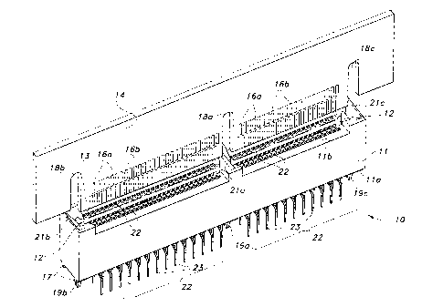
by the reference numeral 10, is illustrated throughout the respective views.
Connector 10
preferably includes a unitarily molded, elongated insulator housing 11
constructed from
any conventional insulative material known in the art. Housing 11 defines a
board-
mounting or terminating face 11 a and a board-receiving face 11 b. The board-
receiving
face l 1b includes an elongate receptacle or card slot 12 for receiving a
mating edge 13 of
a printed circuit board 14. A plurality of contacts 22 (described hereinafter)
are spaced
along both sides of slot 12 for engaging contact pads 16a and 16b adjacent
mating edge
13 on both sides of printed circuit board 14. As shown, contact pads 16a and
16b are in
two rows, with the row of contact pads 16b being closer to edge 13 than the
row of contact
pads 16a. Each of the rows 16a and 16b is generally parallel to mating edge
13. A
polarizing rib 21 a which spans slot 12 and two polarizing shoulders 21 b and
21 c formed
at each end of housing 11 are included for insertion into corresponding
polarizing notches
18a, 18b and 18c in edge 13 of the printed circuit board 14 to ensure the
board in properly
oriented endwise within the slot 12 relative to the elongate connector 10.
In many applications, card edge connectors, such as connector 10, are mounted
on
a second printed circuit board (not shown). The mating circuit board 14 is
commonly
called the "daughter" board, and the second printed circuit board to which the
connector
10 is mounted is commonly called the "mother" board. Connector 10 is
preferably of this
type and includes three boardlocks 19a, 19b, 19c for insertion into
appropriate mounting
holes in the mother board. A plurality of standoffs 17 project downwardly from
board-
mounting face 11 a of housing 11 a predetermined distance in order to space
the housing
11 from the mother board upon placement thereon.
As stated above, connector 10 generally includes a plurality of contacts 22
functionally positioned within housing 11 along each side of slot 12 so as to
operatively
engage the contact pads 16a and 16b on both sides of the daughter board 14.
All of the
contacts 22 include tail portions 23 which project downwardly a predetermined
distance
-5-
CA 02246838 1998-12-03
away from board-mounting face l la for operatively engaging the mother board.
As best
shown in Figs. 3, 6 and 21, the plurality of contacts 22 preferably comprise a
first series
of simple cantilevered beam signal contacts 24 and a second series of dual-
beam ground
contacts 26. Signal contacts 24 are of the conventional type found in card
edge connectors
and may include first and second predetermined shapes as generally shown at
24a and 24b,
respectively.
Referring to Fig. 10, a plurality of dual-beam ground contacts 26 are
preferably
stamped, formed and oriented in a conventional manner out of known sheet
material into
an elongate strip of dual-beam electrical contacts interconnected by a main
Garner strip 27
and a tip carrier strip 28. The contacts 26, as shown, each include a tail
portion 23, a
generally "U" shaped collar portion 29 to which one end of tail portion 23 is
attached, and
two diametrically opposed tips 31a and 31b which diverge from one another at
the
attachment points to collar portion 29. The opposite end of each tail portion
23 is attached
to and lies in the same plane as carrier strip 27. The "U" shaped collar
portion 29 and tips
31a and 31b are formed and oriented, however, so as to lie in a plane
generally
perpendicular to the plane of carrier strip 27. Tip carrier strip 28 may be
attached to tips
31a or 31b. Generally speaking, before insertion into housing 11, carrier
strip 28 is
removed from the contacts 26. Once the contacts are fully seated in housing 1
l, carrier
strip 27 is removed by flexing the strip in relation to the contacts.
Referring to Figs. 11-14, the generally "U" shaped collar portion 29 of
contact 26
includes a bottom or bottoming portion 29a which has a longitudinal axis,
labeled as A-A
in Fig. 14, substantially perpendicular to the plane of carrier strip 27.
Portion 29 further
includes two diametrically opposed portions 29b and 29c which project
downwardly from
portion 29a and converge toward one another whereupon they are attached to
tips 31 a and
31b, respectively. Furthermore, as best illustrated in Fig. 13, contact tips
31a and 31b are
slightly splayed to pre-load the tips before insertion into housing 11, which
assists in
preventing short-circuiting with other contacts in the housing. Therefore, the
splay angle
between the tips, generally designated as 8, is dependent upon the design of
the contact
receiving sleeves or cavities within housing 11 and the proximity of the tips
31a and 31b
to other contacts 24 within housing 11, which for purposes of the present
invention are
-6-
CA 02246838 1999-10-25
known in the art card edge connectors. Also, for illustrative purposes only,
the contacts 26
shown in Figs. 11-14 do not include a realignment twist angle «.
Figs. 7-9, 1'7 and 19 best illustrate housing 11. Housing 11 has two rows of
contact tip seating apertures 32 extending through the board-receiving face
llb for receiving
the tips of contacts 24 and 26 once seated in housing 11. The rows extend
generally parallel
to the longitudinal axis of the housing 11, one row on each of opposite sides
of card slot 12.
Each row includes an alternating series of differently shaped first and second
tip seating
apertures 32a and 32b. Similarly, housing 11 has two rows of contact receiving
apertures 33
extending through the board-mounting face l la for receiving the tips of the
ground contacts 26
during bottom loading into housing 11. Even though these rows extend likewise
generally
parallel to the longitudinal axis of the housing 11, the apertures 33 are
separate or divided by
a center bar 34 formed in board-mounting face l la.
Referring to Figs. 17 and 19, the tips 31a and 31b of the plurality of dual-
beam
ground contacts 26 are bottom loaded into housing 11 through apertures 33.
Fig. 17 shows
only a portion of the total number of contacts 26 partially loaded while Fig.
19 shows only a
portion of the total number of contacts 26 fully seated. In order for the
correct tips 31a and
31b to align with the correct apertures 33, a realignment twist a is added to
the bottoming
portion 29a of the contacts during the stamping or method of manufacture
operation, as shown
in Figs. 15 and 16. The realignment twist a occurs about the longitudinal axis
A-A of portion
29a and is the effective sure of two oppositely oriented twists «, and a2. The
effective angle
of the twist is sufficient to bring tips 31a and 31b into general alignment or
into the plane of
collar portion 29, as shown in Figs. 15 and 16, so that they may be gang
inserted into the
correct apertures 33. Of coarse, the correct apertures 33 are dependent upon
the contact pattern
of the connector. The preferred ground contact pattern for the present
invention is illustrated
throughout the figures, and is best shown in Fig. 17. If the realignment twist
a were not
introduced into the contact<~ 26 prior to insertion into housing 11, they
would not be inserted
correctly, or they would have to be individually inserted. The realignment
twist « disappears
once the contacts) are fully seated in that portion 29a abuttingly engages
center bar 34 which
in effect straightens portion 29a so that it has no twist, allowing tips 31a
and 31b to move to
their pre-loaded positions.
_7_