Note : Les descriptions sont présentées dans la langue officielle dans laquelle elles ont été soumises.
CA 02249131 1998-10-01
RD-25,566
-1 -
HIGH RESOLUTION RADIATION IMAGER
RELATED APPLICATIONS AND PATENTS
This invention was made with Government support under
Government Contract No. MDA 972-94-30028 awarded by DARPA.
The Government has certain rights ih this invention.
TECHNICAL FIELD
This invention relates generally to solid state radiation
imagers and in particular to improved spatial resolution in imagers
having a scintillator coupled to a photosensor array.
BACKGROUND OF THE INVENTION
Soiid state radiation imaging arrays typically comprise a
photosensor array coupled to a scintillator. The radiation to be
detected (e.g., x-rays or the like) penetrates the scintillator and is
absorbed by the scintillator material in an event that results in the
release of optical photons. The photosensor array coupled to the
scintillator is used to detect the optical photons, providing a spatial
location (x,y) in the array that corresponds with the point in the
scintillator at which the incident radiation was absorbed. Readout of
the photosensor array allows electrical signals to be generated that
correspond to the pattern of absorbed radiation. The data embodied
in such electrical signals can be presented in a visual display or
otherwise processed to allow analysis of the radiation, pattern.
Good spatial resolution in an imager necessitates that
the optical photons generated in an absorption event be detected by a
photosensor in the immediate vicinity of the absorption event so that
the electrical signal representing the absorbed radiation originates
from a sensor in the array near the absorption event. Photons
generated in the absorption event, however, are emitted in all
directions and will readily travel through the scintillator material, which
CA 02249131 1998-10-01
RD-25,566
-2- -
typically is substantially optically transparent. The multi-directional
emission of optical photons from an absorption event results in
approximately half of the photons moving in a direction away from the
photosensor array; these photons are not only not directly detected by
the photosensor array but also can be reflected off the surface of the
scintillator opposite the photosensor array along paths that cause
them to strike the photosensor array at a point away from the spatial
location (x,y) of the absorption event, thus degrading the spatial
resolUtion and image quality provided by the imager.
Reduction of optical crosstalk, that is, optical photons
that are incident on the photosensor array at a point distant from the
spatial location (x,y) of the absorption event, is desirable to improve
spatial resolution and image quality.
SUMMARY OF THE INVENTION
A radiation imager includes a photosensor array that is
coupled to a scintillator so as to detect optical photons generated
when incident radiation is absorbed in the scintillator. In accordance
with this invention, the imager includes an optical crosstalk attenuator
that is optically coupled to a first surface of the scintillator (that is, the
surface opposite the photosensor array). The optical crosstalk
attenuator includes an optical absorption material that is disposed so
as to inhibit reflection of optical photons incident on the scintillator first
surface back into the scintillator along selected crosstalk reflection
paths. The crosstalk reflection paths are those paths oriented such
that optical photons passing along such paths would be incident upon
photosensor array pixels that are outside of a focal area
corresponding to the absorption point in the scintillator.
In accordance with the present invention, the imager
further may include an optical screen layer that is optically coupled to
the scintillator second surface so as to be disposed between the
scintillator and the photosensor array. The optical screen layer
CA 02249131 1998-10-01
RD-25,566
-3-
comprises a substantially transparent material having a critical index
of refraction so as to cause preferential reflection of optical photons
that are incident on the screen layer at an angle that would result in
optical crosstalk, typically greater than a scintillator critical angle
determined by the scintillator material and structure .
BRIEF DESCRIPTION OF THE DRAWINGS
Figure 1 is a schematic representation of a radiation
imager photosensor array
Figure 2 is a cross-sectional view of a portion of a
radiation imager in accordance with one embodiment of the present
invention.
Figure 3 is a cross-sectional view of a portion of a
radiation imager in accordance with another embodiment of the
present invention.
Figure 4 is a cross-sectional view of a portion of a
radiation imager in accordance with a further embodiment of the
present invention. -
Figure 5 is a cross-sectional view of a portion of a
radiation imager in accordance with a still further embodiment of the
present invention.
Figure 6 is a cross-sectional view of a portion of a
radiation imager in accordance with an embodiment of the present
invention, which figure illustrates various reflection angles of light
within the imager.
Figure 7 is a cross sectional view of a portion of a
radiation imager in accordance with another embodiment of the
present invention.
CA 02249131 1998-10-01
RD-25,566
-4-
Figure 8 is a graphical representation of reflection
coefficient as a function of angle of incidence of light passing between
cesium iodide and silicon oxide.
r'l DE T AiLED DESCi=sir T iON OF THE INVENTION
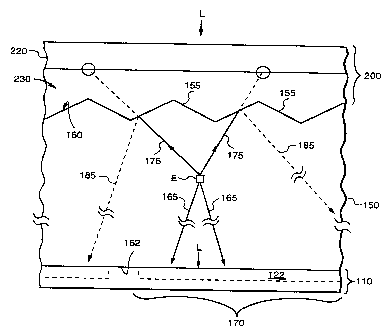
A solid state radiation imager 100 typically comprises a
photosensor array 110 having a plurality of pixels 120 disposed in
rows and columns, as illustrated in Figure 1. Photosensor array 110 is
optically coupled to a scintillator 150 (Figure 2) that is disposed over
the photosensor array. In operation, imager 100 is positioned so that
radiation to be imaged, for example x-rays and the like, is incident on
scintillator 150, which typically comprises a material such as cesium
iodide or the like. Incident radiation typically enters scintillator 150
across a first surface 160 and is absorbed in the scintillator material in
an event resulting in the generation of optical photons. Detection by
photosensor array 110 of the optical photons emitted when the
incident radiation is absorbed by the scintillator material enables the
generation of an electrical signal corresponding to the pattern of the
incident radiation.
In photosensor array 110, each pixel 120 comprises a
photosensor 122, such as a photodiode, that is coupled via a
switching device 124 to address lines 126, 128. The switching device
124 typically comprises a thin film field effect transistor ("TFT" or
"FET"); commonly address line 126 is referred to as a scan line and is
coupled to the respective gate electrodes of TFTs 124 in pixels
disposed along a row in photosensor array 110. A signal applied to a
scan line causes TFT 124 to become conductive, thereby allowing an
electrical signal on photosensor 122 to be read out from address line
128, commonly referred to as a data line.
Optimally, all optical photons generated from the
absorption of a photon of incident radiation are detected by pixel 120
in photosensor array 110 that corresponds most closely with the
CA 02249131 1998-10-01
RD-25,566
-5-
spatial (x,y) location of the emission location (illustrated as "E" in
Figure 2). As used herein, spatial location corresponds to the location
"L" (figure 2) that has coordinates (x,y) in the plane of photosensor
array 110 (for purposes of reference, and not limitation, the orientation
of imager 100 is referred to in this document in the horizontal plane),
regardless of the distance that the incident radiation photon has
penetrated through the thickness of, scintillator 150 prior to absorption
(e.g., in the plane orthogonal to the horizontal plane, referred to as the
vertical plane).
As the material comprising scintillator 150 is substantially
optically transparent (at the wavelength of the generated photons),
optical crosstalk can degrade spatial resolution of the imager. As
used herein, "optical crosstalk" refers to optical photons generated in -
an absorption event at a given spatial location (x, y) in the scintillator
being detected by a photosensor array pixel other than the pixel in
closest proximity to the spatial location of the absorption event.
"Spatial resolution" and the like refers to the ability of the imager to
produce an electrical signal that accurately corresponds with the
spatial pattern of incident radiation (one of the significant determinants
of the accuracy of the signal is the detection of optical photons by
primarily the photosensor pixel in closest proximity to the absorption
event).
In accordance with the present invention, imager 100
further comprises an optical crosstalk attenuator 200 that is disposed
over _a first surface 160 of scintillator 150. As used herein, "over",
"above", "under" and the like are used to refer to the relative location
of elements of imager 100 as illustrated in the Figures and is not
meant to be a limitation in any manner with respect to the orientation
or operation of imager 100. Optical crosstalk attenuator 200 is
optically coupled to scintillator 150 (that is, disposed in a position so
that optical photons passing upwards out of scintillator 150 across first
surface 160 will be incident on crosstalk attenuator 200) so as to
inhibit reflection of optical photons incident off of scintillator first
CA 02249131 1998-10-01
RD-25,566
-6-
surface 160 back into scintillator 150 along crosstalk reflection paths
185, as described more fully below. In Figure 2, optical crosstalk 200
is illustrated with a backing plate 220; this representation is provided
by way of illustration and not limitation with respect to the various
embodiments of crosstalk attenuator 200 set forth below.
By way of example and not limitation, as shown in Figure
2, incident radiation absorbed in scintillator 150 results in emission of
optical photons at position "E." Optical photons emanate from position
"E" in all directions; desirably, optical photons emanating from position
"E" are detected within a focal area 170 that corresponds to the
dimensions of pixel photosensor active area 122 disposed in closest
proximity to the spatial location "L" of the absorption location "E" of the
incident radiation (e.g., in Figure 2, "L" is illustrated directly under the
location of absorption event "E"). For example, optical photons
passing along direct paths 165 will be incident on pixel 120 in focal
area 170. Optical photons passing along exemplary indirect paths
175, however, are incident upon scintillator first surface 160. In the
absence of crosstalk attenuator 200, such photons commonly would
be reflected from surface 160 along illustrative crosstalk reflection
paths 185. Crosstalk reflection paths 185 refer to paths on which
optical photons are reflected from scintillator first surface 160 and that
are oriented such that the photons would be incident on portions of
photosensor array 110 outside of focal area 170.
One embodiment of optical crosstalk attenuator 200 for
use with a scintillator with a smooth first surface 160 is illustrated in
Figure 3. In this embodiment, scintillator first surface 160 is smooth,
such as a polished surface, typically having a surface roughness much
less than the wavelength of the incident light (e.g., less than about and
order of magnitude of the wavelength k (e.g., a/10)). For such a
scintillator arrangement, optical crosstalk attenuator 200 typically
comprises an optical absorption material 210 disposed on a backing
member 220, with attenuator 200 being disposed over scintillator 150
such that absorption material 210 faces scintillator first surface 160.
CA 02249131 1998-10-01
RD-25,566
-7-
Optical absorption material 210 typically has an optical transmittance
in the range between about 25% and about less than 1%.
Additionally, optical absorption material desirably exhibits a low
absorption cross-section for the type of incident radiation to be imaged
by imager 100; for example, for x-ray imaging, it is desirable that
materials disposed above scintillator first surface absorb less than a
few percent of the incident x-ray beam. By way of example, and not
limitation, such absorption material 210 comprises a flat black paint
that is disposed as an overcoat on backing member 220 with a
thickness in the range between about 10 m and about 1 m. Backing
member 220 desirably also exhibits a low absorption cross section for
the radiation being imaged, as noted above. Backing member 220
commonly comprises a thin polyester sheet (or alternatively, a
graphite or plastic plate) having a thickness in the range between
about 1 mm and about 5 m. Optical photons incident on crosstalk
attenuator 200 typically are absorbed (e.g., at location "A" in Figure 3),
precluding the photon being reflected back down into the scintillator
along a crosstalk path 185.
Scintillator 150 used in imager 100 may alternatively
have a needle-like structure, with the needles being oriented in the
vertical plane, extending from a scintillator second surface 162 (which
surface is disposed facing photosensor array 110) towards scintillator
first surface 160. Such a scintillator structure is formed by control of
the deposition process of the scintillator material (e.g., Csi) over
photosensor array 110. This needle-like structure serves to localize
optic-al photons generated when incident radiation is absorbed; spatial
localization is provided because some fraction of the optical photons
generated will undergo total internal reflection within the needle so
that they exit scintillator second surface within the desired focal area
170. Typically such needle formations have an approximate diameter
in the range of about 1 Nm to about 10 pm; consequently, a plurality of
needle structures are disposed over any one pixel 120 in photosensor _
CA 02249131 1998-10-01
RD-25,566
-8-
array 110 (the lateral dimensions of a pixel in such arrays are typically
in the range between about 30 m and about 1 mm).
A needle-like scintillator structure 200 (Figure 2) has a _
scintillator first surface 160 comprising a plumility of columnar
protrusions 155. First surface 160 has an uneven (or textured) finish,
which is not polished in order to maintain the integrity of respective
needle-like structures in scintillator 150. In accordance with the
present invention, especially for use with scintillator having protrusions
155 on first surface 160, optical crosstalk attenuator 200 further
comprises an optical coupling layer 230 that is disposed between
scintillator first surface 160 and optical absorption material 210.
Optical coupling material 230 typically comprises a material such as a
pressure sensitive adhesive (PSA) (e.g., PSA part number V320 of
FLEXcon Co. of Spencer, MA.) that is relatively optically transparent
(e.g., having an optical transmittance in the range between about 50%
and about 100%). Desirably, standard water-based PSA used for
optical coupling material exhibits an index of refraction that
corresponds to the optical index of refraction of the scintillator material
(e.g., has an index of refraction -having a value within t20% of the
value of the index of refraction of the scintillator). Due to the effects of
total internal reflection, it is preferable for the coupling material to
have an index of refraction greater than the index of refraction of the
scintillator, although materials with lower indices of refraction will also
provide acceptable performance. For example, Csl exhibits an index
of refraction of about 1.79; effective optical coupling materials for use
with Csl desirably have respective indices of refraction in the range
between about 1.79 and about 2.15; materials with and index of
refraction in the range between about 1.79 and 1.43 are also
acceptable.
Optical coupling material 230 additionally desirably has a
viscosity such that when it is disposed over the textured scintillator
first surface 160 it is viscous enough to be displaced so as to be in
intimate contact with all surfaces of columnar protrusions 155. As
CA 02249131 1998-10-01
RD-25,566
-9-
used herein, "intimate contact" and the like refers to material being
disposed adjacent to scintillator first surface 160 so that optical
photons pass directly from scintillator first surface 160 into the optical
coupling material (without passing through intermediate air pockets)
over an area greater than about 50% of said first surface. Optical
coupling layer 230 typically has a thickness in the range between
about 10 m and about 1 mm
In a further embodiment of the present invention as
illustrated in Figure 4, an optical absorption material is mixed into
optical coupling layer 230 (as illustrated by speckling in coupling layer
230 in Figure 4). The addition of optical absorption material, such as
fine carbon powder, to optical coupling layer 230 causes coupling
layer 230 to become another absorbing layer, typically exhibiting a
"single pass" optical transmittance in the range between about 40%
and about less than 1% (to reenter the scintillator in the event of
reflection off of absorption material 210, optical photons would need to
pass two times through the absorbing optical coupling layer 230; thus
even a material with a transmittance as high as 40% assures that less
than 16% of the light would reenter the scintillator). One example of
such an absorbing coupling layer 230 comprises fine carbon dust
(e.g., a particle size in the range between less than about 1 m and
about 10 m) mixed with adhesive material.
A still further embodiment of an optical crosstalk
attenuator 200 in accordance with the present invention is illustrated
in Figure 5 and comprises a optical coupling layer 230 that is weakly
absorbing and an optical reflecting layer 240 disposed over the weakly
absorbing coupling layer 230. As used herein, "weakly absorbing"
refers to an optical transmittance in the range between about 90% and
about 40%. It is to be noted that these transmittance figures represent
transmittance for one pass through optical coupling layer; as
described herein, in the present embodiment and optical photon
leaving scintillator first surface 160 would pass twice through coupling
layer 230 before re-entering scintillator 200 across scintillator first
CA 02249131 1998-10-01
RD-25,566
-10-
surface 160. In this arrangement, optical photons emanating from
incident radiation absorption location "E" that are incident on
scintillator first surface 160 will typically pass into weakly absorbing
coupling layer 230. Those photons that enter at angles that result in
relatively short paths (illustrated as path 255 in Figure 5) through
weakly absorbing optical coupling layer 230 will strike reflecting layer
240 and reflect along paths that typically will result in the reflected
photon being incident on photosensor array 110 within the desired
focal area 170 (Figure 2). Conversely, photons entering weakly
absorbing coupling layer along optical crosstalk paths 265 (Figure 5)
will pass a greater distance through the weakly absorbing optical
coupling layer and thus are more likely to be absorbed in layer 230
before re-entering scintillator 150. Adjustment of the optical
transmittance of coupling layer 230 (such as by changing the
concentration (e.g., during fabrication) of optical absorbing material in
coupling layer 230) enables the "tuning" of optical crosstalk attenuator
to provide a desired spatial resolution (e.g., reduction of optical
crosstalk) while still capturing some number of the optical photons that
are emitted along paths towards scintillator first surface 160.
Alternatively, the reflectivity of reflective layer 240 can also be
adjusted in fabrication to provide a desired tuning effect for optical
crosstalk attenuator 200.
Placement of optical crosstalk attenuator over scintillator
first surface 160 in an imager provides a desirable improvement in
imager performance. For example, as is known in the art, one
measure of imager performance is the mod'ulation transfer function
("MTF"). By way of example and not limitation, the following
information provides a comparison of 1) an imager having a reflective
film (alone) in intimate contact with scintillator first surface 160; 2) a
smooth piece of graphite (gray in color) placed above (e.g., about 200
pm) scintillator first surface 160; and 3) an optical crosstalk attenuator
in accordance with the present invention comprising a clear optical
coupling layer with an optical absorption layer thereover (black
CA 02249131 1998-10-01
RD-25,566
-11-
polyester substrate with a clear pressure sensitive adhesive (PSA)
disposed over scintillator first surface 160). MTF's for the three
imager arrangements were measured (at the spatial frequency of 2.5
lp/mm) and are summarized below:
Scintillator Surface Coverina MTF Relative Improvement
Highly reflective 0.2 0%
Gray graphite/air gap 0.241 20%
Black with clear PSA 0.314 57%
The optical crosstalk attenuator in accordance with this
invention provides improved imager performance and serves to reduce
the number of optical photons that reflect off scintillator first surface
160 and propagate through the scintillator along crosstalk reflection
paths.
Performance of imager 100 can be further enhanced in
accordance with this invention with an optical screen layer 300
optically coupled to scintillator second surface 162 (Figures 6 and 7)
that is disposed facing photosensor array 110 (that is, is disposed
opposite scintillator first surface 160). Optical screen layer 300
comprises a substantially transparent material (e.g., having an optical
transmittance greater than about 80%); screen layer 300 material is
further selected to have an index of refraction that is less than that of
the scintillator material. This lower value of the index of refraction for
the screen layer 300 with respect to the value of the index of refraction
of the scintillator material results in some portion of the optical photons
that are incident on said screen layer from the scintillator second
surface being reflected back into scintillator 150. The lower the value
of the index of refraction with respect to scintillator 150, the greater the
proportion of incident optical photons that will be reflected back into
scintillator 150 (that is, the optical photons undergo total internal
CA 02249131 1998-10-01
RD-25,566
-12-
reflection in the scintillator). Selection of a material for screen layer
300 having a particular index of refraction thus enables one to "tune"
the proportion of internal reflection; such tuning enables design
choices to be made between anticipated MTF increases (resulting
from reduced optical crosstalk) and corresponding signal level
decreases (e.g., reduced numbers of optical photons reaching the
photosensor array).
Use of screen layer 300 for "tuning" an imager as
described above is particularly applicable when a scintillator material
such as cesium iodide is used. The tuning process is refined through
selection of a screen layer having a critical index of refraction to
provide reflection of optical photons striking screen layer 300 at an
angle greater than a scintillator critical angle so as to provide
reasonably precise demarcation of photons that will be reflected as
undesirable crosstalk light and photons that will be able to pass
through screen layer 300 into photosensor array 110. As used herein,
"critical index of refraction" and the like refers to a value of screen
layer's index of refraction that is less than the value of the scintillator
index of refraction by an amount that results in reflection of incident
photons striking the screen layer at an angle greater than a scintillator
critical angle. "Scintillator critical angle" and the like refers to the
angle of incidence for photons passing from scintillator second surface
at which reflection will occur off of screen layer 300 back towards
scintillator 150. The scintillator critical angle has a value that is
selected to reduce optical crosstalk in the scintillator as described
more-#ully below.
In an imager having a cesium iodide scintillator, optical
screen layer 300 typically comprises silicon oxide, a material that
provides desirable optical transparence (e.g., < 1% absorption), is
readily uniformly deposited in the fabrication process (e.g., in a
plasma enhanced chemical vapor deposition (PECVD) process), and
exhibits an optical index of refraction of about 1.5 that provides a
desired scintillator critical angle for reflecting photons passing from
CA 02249131 1998-10-01
RD-25,566
-13-
scintillator second surface. Alternatively, materials such as
magnesium fluoride (MgF2), and polyimide can be used as appropriate
to provide different scintillator critical angles. Optical screen layer 300
typically has a thickness sufficient to produce significant reflection
(e.g., reflection of about 50% or more optical photons incident at angle
equal to or greater than the scintillator critical angle) while being thin
enough to prevent spatial resolution degradation (e.g., due to the
lateral spread of light). Common thicknesses for optical screen layer
300 comprising silicon oxide are in the range between about 25 nm -
and about 5 m.
In accordance with this invention, optical screen layer
300 can be effectively used with any scintillator structure. Screen
layer 300, however, is particularly effective when used with
scintillators that are not highly scattering, such as a scintillator that
has a plurality of columnar protrusions (or needles) 152 from the
scintillator surface (illustrated in Figure 6 as parallel lines in the
vertical plane within scintillator 150). Columnar protrusions 152 serve
to isolate a portion of the optical photons emanating from the location
"E" of an absorption event. The long thin needle-shaped structure of
columnar protrusion 152 (e.g., having a diameter in the range between
about 5 m and about 10 m, and a length in the range between about
50 m and 1000 m) serves to trap virtually all light that is emitted at
an angle greater than a critical angle determined by the interface
between the Csf column 152 and the material surrounding the column.
For example, if air surrounds the column, the critical angle is about 34
degrees; thus all light photons striking the column sidewall at or
greater than an angle of incidence of 34 degree will undergo total
internal reflection within the needle column. As illustrated by pathway
"T" in Figure 6, this light will pass though columns 152 and strike
scintillator second surface 162 at an angle between about zero
degrees (perpendicular to the surface) and about 56 degrees (with
respect to the normal). As this light accurately represents the spatial
CA 02249131 1998-10-01
RD-25,566
-14-
(x,y) location of the absorption event, it is desirable that these optical
photons pass through screen layer 300 to photosensor array 110.
Optical photons that strike the sidewall of columnar
protrusion 152 at an angle less than the critical angle will pass outside
of columnar protrusion 152. As noted above, the critical angle is
about 34 degrees for scintillator needles comprising cesium iodide
(index of refraction 1.79) surrounded by an air gap (index of refraction
1.00). Photons passing from columnar protrusion 152 that strike
scintillator second surface 162 thus will have an angle of incidence of
56 degrees or greater (the "scintillator critical angle", denoted as "CA"
in Figure 6), with the scintillator critical angle being measured from the
normal of second scintillator surface 162 to the path of incident
photon. Figure 8 illustrates graphically the effective reflection
coefficient of the Csl to optical screen interface (for SiOx), indicating
the scintillator critical angle occurring at 56 degrees, at which nearly
total reflection occurs. Optical screen 300 comprises a material
having a critical index of refraction, that is, an index of refraction that
will cause reflection of photons striking the optical screen at the
scintillator critical angle. Thus, substantially all photons escaping from
columnar protrusion 152 and which pass from scintillator second
surface 162 will be reflected by optical screen 300 back into scintillator
150.
Optical screen 300 is commonly disposed immediately
adjacent to scintillator second surface 162 (that is, no intervening
material layers). Alternatively, optical screen 300 is optically coupled
to scintillator second surface 162 via intervening layers 50 (Figure 7)
of material, such as silicon nitride (SiN) (typically having an index of
refraction between about 1.9 and 2.0) that are, for example, disposed
adjacent to scintillator 150 to provide environmental protection to the
scintillator material. As long as such intermediate layers have an
index of refraction greater than that of Csl (e.g., about 1.84 to about
2.1), the presence of such intervening layers does not adversely affect
the ability of optical screen to reflect optical photons leaving scintillator
CA 02249131 1998-10-01
RD-25,566
-15-
second surface 162 at the scintillator critical angle (or angles less than
the scintillator critical angle).
Imager 100 beneficially, but not necessarily, comprises
both optical crosstalk attenuator 200 and optical screen layer 300, as
illustrated in Figure 6.
It will be apparent to those skilled in the art that, while
the invention has been illustrated and described herein in accordance
with the patent statutes, modifications and changes may be made in
the disclosed embodiments without departing from the true spirit and
scope of the invention. It is, therefore, to be understood that the
appended claims are intended to cover all such modifications and
changes as fall within the true spirit of the invention.