Note : Les descriptions sont présentées dans la langue officielle dans laquelle elles ont été soumises.
CA 02249670 1998-10-0~
GLASS WAVE GUIDE ELEMENT AND METHOD OF
MANUFACTURING THE SAME
BACKGROUND OF THE INVENTION
The present invention relates to a glass wave guide
element and a method of manufacturing a glass wave guide
element.
Wavelength divisional multiplexing (WDM) communications
have been increasingly employed in recent years, as a result
of the development of optical communication technology. In
order to separate wavelength multiplexing light transmitted
inside an optical fiber, communication of this kind requires
an element which can select whether light having a certain
wavelength is allowed to pass through or to be reflected by
the element.
An element of this kind currently exists, wherein an
ultraviolet light is irradiated onto a wave guide having an
optical fiber containing germanium to form a diffraction
grating along a light transmission direction in the fiber by
inducing refractive index change. Further, the Bragg
wavelength is changed by changing the temperature on the
grating by heating the wave guide using a heater.
However, as a result of the manufacturing complexities
involved in mounting the heater, conventional wave guide
elements employing optical fiber tend to be very expensive.
Further, conventional wave guide elements are generally
unable to meet the reduction in size and increase in
integration requirements of wavelength divisional
multiplexing (WDM) communications. In addition,
conventional wave guide elements do not provide sufficient
cost effectiveness or productivity to meet a future increase
in wavelength divisional multiplexing communications from 16
channels to 32 channels.
SUMMARY OF THE INVENTION
An object of the present invention is to provide a
glass wave guide element which is small, easily integrated
CA 02249670 1998-10-0~
and easy to mass produced, and a method of manufacturing the
same wherein the above-mentioned problems are solved.
It is an object of the present invention to provide a
glass wave guide element comprising a substrate; an under
cladding formed on the substrate; a core having a
diffraction grating of a spatially periodically changing
refractive index along a light transmission direction,
wherein the core is formed on the under cladding; an over
cladding covering the core; and a heater for changing the
Bragg wavelength of the diffraction grating, wherein the
heater is arranged in the over cladding, and the core and a
central portion of both claddings in a surrounding portion
of the core are formed in a state continuously separated
along a longitudinal direction of the core from the
substrate, through a gap; and the core and the surrounding
portion of the core are formed in a state separated in a
width direction of the core from a surrounding portion of
both claddings, through a gap.
It is a further object of the present invention to
provide a glass wave guide element comprising a heater
formed of a metallic laminated film for changing the
temperature of the core; the heater being formed along an
upper surface of the over cladding in the inside portion
surrounded by the gaps; and an opening for irradiating
ultraviolet light to produce a spatially periodically
changing refractive index in the core; wherein the opening
is formed in a central portion of the heater.
It is a further object of the present to provide a
glass wave guide element formed by a titanium film formed on
the over cladding and a platinum film formed on the titanium
film.
It is a further object of the present invention to
provide a heater in the glass wave guide element which is
formed such that a pad zone to be wire-bonded to the heater
is a three layer film formed of titanium, platinum and gold,
and a heating zone of the heater is a two-layer film formed
of titanium and platinum.
CA 02249670 1998-10-0~
It is a further object of the present invention to
provide a method of manufacturing a glass wave guide element
comprising the steps of forming a thin film on a substrate;
forming a terrace by adjusting the thin film to a desired
optical path to perform patterning; successively forming an
under cladding, a core and an over cladding on the terrace;
spatially intermittently forming gaps in both sides of the
core along said core to a depth reaching the terrace; and
forming a diffraction grating of a spatially periodically
changing refractive index along a transmitting direction of
light in the core by continuously removing the terrace along
a longitudinal direction of the core by inserting a
substance capable of etching the terrace from the gaps.
In accordance with one aspect of the present invention,
the thin film is formed of silicon.
It is a further object of the present invention to
provide a method of manufacturing a glass wave guide element
wherein a pit formed by the gaps penetrating through the
over cladding and the under cladding is used as a flow pass
of the etching substance for removing the thin film during
manufacturing and functions as a heat insulating structure
for preventing heat dissipation to a surrounding portion in
a lateral direction of the core after completion.
In accordance with another object of the present
invention there is provided a method of manufacturing a
glass wave guide element further comprising the steps of
forming a heater along the core on an upper surface of the
over cladding, in the inside portion surrounded by the gaps,
for changing the temperature of said core; wherein the
heater is formed of a metallic laminated film; and forming
an opening for irradiating ultraviolet light to produce a
spatially periodical refractive index in the core in a
central portion of the heater.
Another object of the present invention is to provide a
method of manufacturing a glass wave guide element wherein
CA 02249670 1998-10-0~
the heater is formed by forming a titanium film on the over
cladding and then forming a platinum film on the titanium
film.
Further still, it is an object of the present invention
to provide a method of manufacturing a glass wave guide
element wherein the heater is formed by forming a
three-layer film of titanium, platinum and gold by either of
the etching or lift-off method; and wherein a pad zone for
performing wire-bonding is formed in a three-layer film,
when left alone; and a heater zone is formed in a two-layer
film by removing only the gold film portion.
BRIEF DESCRIPTION OF THE DRAWINGS:
These and other objects, features and advantages of the
present invention will be understood more clearly from the
following detailed description with reference to the
.
accompanylng drawlngs, whereln:
FIG. 1 is a schematic perspective view showing an
embodiment of a glass wave guide element in accordance with
the present invention; and
FIG. 2 is a process diagram, (a) to ( g ), showing a
method of manufacturing the glass wave guide element shown
in FIG. 1.
DETAILED DESCRIPTION OF THE PRESENT INVENTION
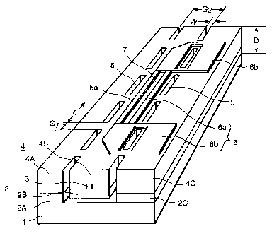
FIG. 1 is a schematic perspective view showing an
embodiment of a glass wave guide element in accordance with
the present invention. Explanation will be made using
numerical values, but it is not limited to the values. An
under cladding 2 (2A, 2B, 2C) is formed on a quartz
substrate 1, and a core 3 having a diffraction grating of a
spatially periodically changing refractive index along a
direction of transmitting light. The core 3 is covered with
an over cladding 4 (4A, 4B, 4C). There is formed a gap
(pit) 5 having a U-shaped cross-section by which the core 3
and a central portion (2B, 2C) of both claddings surrounding
CA 02249670 1998-10-0~
the core are spatially intermittently separated from the
quartz substrate 1 and the surrounding portion (2A, 2C, 4A,
4C) of the both claddings.
The gap 5 having a U-shaped cross-section is
intermittently spaced. However, between the under cladding
2B and the quartz substrate 1 under the core 3 there is a
gap 5 over the total length in the longitudinal direction of
the glass wave guide element. The gap is formed by a method
described hereinbelow.
At a position on the over cladding 4 corresponding to
the core 3, a heater 6 for changing the Bragg wavelength of
the diffraction grating is provided. Between portions 6a,
in the central portion of the heater 6, there is formed an
opening 7 for irradiating ultraviolet light to produce a
spatially periodic change of the refractive index in the
core 3. The reference character 6b indicates a pad zone for
applying voltage to the heater 6. As an example, the width
W of the pit 5 is approximately 20 ~m, the length L is
approximately 3.3 mm, the depth D is approximately 40.5 ~m,
and the gap G1 in the longitudinal direction of the pit 5 is
approximately 0.2 mm, the gap G2 in the longitudinal
direction of the pit 5 is approximately 130 ~m.
The core 3 and the central portion (2B, 4B) of both
claddings are separated from the substrate 1 and the
surrounding portion (2A, 2C, 4A, 4C) of both claddings
through a gap 5, and the gap 5 functions as a heat
insulator. Since dissipation of heat is suppressed by the
gap 5, heat of the heater 6 is effectively used in the
temperature control of the core 3. Therefore, the element
can be made smaller in size and the degree of integration of
the element can be increased.
FIG. 2 is a process diagram, wherein steps (a) to (g),
illustrate a method of manufacturing the glass wave guide
element shown in FIG. 1.
A thin silicon film 8 having a thickness of
approximately 2.5 ~m is formed all over the quartz substrate
1 by a sputtering method (not shown in the figure). The
CA 02249670 1998-10-0~
thin silicon film 8 is patterned by photo-lithography as a
silicon terrace 8 (FIG. 2 (a)). A quartz under cladding 2
having a thickness approximately 8 ~m is formed using plasma
CVD (FIG. 2 (b)).
A germanium containing core film having a thickness of
approximately 6 ~m is formed all over the surface of the
under cladding 2 using the sputtering method (not shown in
the figure), and a core (light path) 3 is formed by
lithography (FIG. 2 (c)). An over cladding 4 is formed
having a thickness of 30 ~m by a frame accumulating method
(FIG. 2 (d)).
A heater 6 comprising three layers, including a
titanium layer having a thickness of approximately 0.1 ~m, a
platinum layer having a thickness of approximately 0.5 ~m
and a gold layer having a thickness of approximately 0.5 ~m
is formed by lithography. However, a heating zone 6a is
formed in a two-layer structure by removing the gold layer
by etching (FIG. 2 (e)). An opening 7 is formed in the
middle portion of the heating zone 6 (between 6a, 6a).
Next, pits 5 are formed in both sides of the heater 6 by
etching. The etching of the pits 5 is performed so as to
reach the silicon terrace 8 (FIG. 2 (f)). By the pits 5,
the claddings 2, 4 are separated into a central portion
(2B, 4B) and surrounding portions (2A, 2C, 4A, 4C). The
claddings 2, 4 continue in the width direction at positions
where the pits 5 are not formed.
Then, all of the silicon terrace 8 is removed over the
total length in the longitudinal direction of the glass wave
guide element by etching (FIG. 2 (g)). That is, an etching
substance for removing the silicon terrace 8 is introduced
through the pits 5 to remove all the silicon terrace 8.
Many glass wave guide elements are formed on a quartz
substrate at a time through the course of the method as
described above, and subsequently diced and separated into
respective elements. Then, the Bragg grating is formed in
the core 3 by an irradiating excimer laser to obtain a glass
wave guide element as shown in FIG. 1.
.
CA 02249670 1998-10-0~
In order to check the characteristics of the element
manufactured by the method according to the present
invention, the Bragg wavelength shift was confirmed by
conducting current to the heater 6. For example, the
wavelength shift was 0.4 nm toward the long wavelength side
at a heater current of 80 mA. This characteristic is
equivalent to that of the conventional element.
Silicon is a preferred material for use as the thin
film as it easily forms a film, has a high heat resistance,
provides a good compatibility with a quartz material as well
as displaying comparatively easy and safe etching
selectivity to quartz in the manufacturing process.
Chromium is generally used as a heater material, however
chromium cannot be used in this case since ultraviolet
light, that is, the excimer laser, is irradiated after the
heater is formed.
Platinum was selected on the basis of being a high
melting-point metal capable of withstanding the laser
irradiation, a less reactive and stable metal, a metal
particularly resistant to oxidizing, and having a electric
resistivity capable of being used as a heater material.
Accordingly, it was confirmed by tests and evaluation that
platinum was the most suitable material. However, since
platinum is weak in adhesiveness to glass, titanium is
inserted between them to increase the adhesiveness.
Therefore, it is necessary to make the heater in a two-layer
structure.
Thus, the present invention can provide a glass wave
guide element and a method of manufacturing the glass wave
guide element which can cope with the increasing
multiplicity of wavelength divisional multiplexing
communications, which has the same characteristics as those
of the conventional element using an optical fiber, and is
small in size, easily integrated and easily mass produced.
Although germanium is used as the additive to the core
in an embodiment of the present invention, this additive is
not limited to germanium and the same effect can be attained
CA 02249670 1998-10-0~
by adding an element producing an induced refractive index
change to ultraviolet light, for example, phosphorus.
Further, other methods may be employed as the method of
film-forming the under cladding, the core and the over
cladding.
In accordance with the glass wave guide element
described above, the core covered with the under cladding
and the over cladding of the glass wave guide and the
central portion of the claddings in the surrounding portion
of the core are formed in a state continuously separated
along the longitudinal direction of the core, from the
substrate through the gap, and the core and the surrounding
portion thereof are formed in a state separated in the width
direction of the core from the surrounding portion of the
claddings through the gap. Therefore, the element can be
easily made in a smaller size and having a high degree of
integration. Further, it is easy to form the gaps and to
remove the thin film using the gaps. Therefore, the present
invention provides a glass wave guide element and a method
of manufacturing the glass wave guide element in a manner
suitable for mass production.