Note : Les descriptions sont présentées dans la langue officielle dans laquelle elles ont été soumises.
SEP. -25' 98(FRI) 08.37 HILL S'fEADMAN
P. 011
FI! ~'. ''~TIlIS Ai~lfi~"BfB
---~ , ~ll~ISLATION
Specification
Circuit arrangement for the regeneratim of an input signal
containing digital data sequences
The invention relates to a circuit arrangement, in particular
for wireless telecommunication apparatuses according to the
DUCT standard, for the regeneration of an input signal
containing characteristic digital. data sequences.
In today's data processing installaticns, communication
apparatuses and communication systems, the transmission,
storing and processing of data or, respectively, items of
information increasingly take place with the aid of digital
Z5 technology. Data or, respectively, i.~lems of information are
thereby stored as sequences of disc.re~te values. This digital
coding is based in most cases on a binary representation, in
which the allowed range of values is :invited to two different
discrete values, designated as a rule as "HTGH," or,
respectively, "1, " and "I:,OW, " or, rest ~ectively, "0 , " The
individual elements ox, respectively, positions in a data
sequence Coded in this way are design~~ted in binary coding as
"bits" (from b~na.ry digit? - I~owever, alongside this digital
representations are also used. with th:ee or more different
discrete values in the allowed value -ange.
zf a sequence of digital values is xe~resEnted as an e.g.
electrical signal, a s~.gnal curve results from a sequence of
signal impulses that respectively refresent a position of the
underlying digital value sequence. 1n the ideal case, all
impulses representing the same dic~it~l value are thereby
identical to one another, and differ clearly, e.g. in form car
level height, from impulses that repoesent other digital
values, nn this way, each digital value is reversibly and
unambiguously allocated to a apoclfi: type of impulse.
1
CA 02250061 1998-09-25
SEP. -25' 98(FRI) 08:34 HILL STEADMAN
P. 002
In digital technology, one very often makes use of a coding In
the form of what axe called "rectangul.ir impulses" that are
equally long among themselves, whereby each ~.mpulse comprises
a signal level that is constant within a range of tolerance
and whose height characterizes it. Fo: 'the signal level, only
discrete values are thereby allowed, whose number is equal to
the number N of different values in the underlyXng digital
range of values, whereby each d~.gital value is reversibly and
unambiguously allocated to one of the signal levels.
In the transmission, storing ox processing of digitally coded
data or, respectively, items of information with the aid of
(general~.y electrical or optical) signals, in practice
disturbances constantly occur that lead to deviations from the
ideal signal curve. If these deviaticns, e.g. due to repeated
transmission of a signal, become too aarge, the underlying
digital value sequence can no longer re recovered
unambiguously from the signal, and ma-functions occur. In
general, this problem is countered by regenexati.ng the
ZO corresponding signals, e.g. after a t:ansmiss~.on via a
transmission path or during the reading out from a memory,
using corresponding means, whereby the original signal curve
is reproduced to the greatest possib~.~ extent.
From EP a 133 067 A1, e.g. such an ap?aratus is known for the
regeneration of a readout signal from optical storage
diskettes, which comprises for the ccrrection of a readout
clock signal. a deformatl.on circuit cc nneCted after a .readout
processor.
The regeneration of digital signal° :s also used in wireless
telecommunication apparatuses operated for examp~.e acCOrd~.ng
to the digital DECT standard, in order to free the signals
transmitted via radio between 'the base station and the mobile
CA 02250061 1998-09-25
__ SEP, -25' 98(FRI) 08.35 HILL STEADMAN
P. 003
part (or, respectively, the mobile pawl and the base station)
from disturbances that occur thereby.
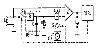
A corresponding circuit arrangement fog ACCT systems -- Figure
1 -- is disclosed in DE 42 36 774 C2. fhe binary-coded signal.
to be regenerated, designated the input, signal Ue in the
following, is thereby supplied to an analog compaxator K,
which compares it with a reference lev~ll UI,, and outputs, at
its output, the signal UA, regenerated in a sequence of equal~.y
long rectangular ~.mpulses with identi.c~l bit structure. The
reference level LTI~ is obtained by means of segment-by-segment
integration of the input signal UE by r.eans of an integration
element IG.
The fact is thereby exploited that, ae~ordi~ng td the DDCT
standard, in each transmission channel the synchronous
~.nit.ializer word, which comprises the First 16 bits of a
transmission frame consisting of. X20 fits and which serves for
synehroniza~ion together with the synchronous acknowledgment
word comprising the subsequently fQllcwing 16 bits, represents
a characteristic data sequence. It ccrlsists of a periodic
alterriatlng bit sequence of HIGH and IOW values, which for the
transmission direction "mobile station - base station" begins
with "1010..." and for the reverse transmission direction
"base station - mob~.le station" begins with "010....." The
i.ntegratian of an input signal U~, -- F'igu~e 3a -- respectively
extends only to this characteristic bit sequence, and is
braked off with the aid of a switch S., driven by a checking
apparatus CTRL, if after 'the synchronous initial~.zer word two
identical bit values follow one another in succession for the
first time. In this way, there resu7is ~~ Figure 3b ~-- a
reference level C7~G, approximately at the height of the average
value U~~ of the HIGH and TOW levels ~ ~f the input signal U~,
which is stable during the regenerat..on of the subsequently
CA 02250061 1998-09-25
SEP, -25' 98(FRI) 08.37 HILL S'fEADMAN P. 012
following signal curve. However, a disadvantage of the
disclosed solution is that the first kiv value identical to
the immediately preceding one ~.s not recognized until
integration has already taken place offer the associated signal
impulse, whereby a reference level TJT~ results that is offset
in relation to its previous value Un~. This undesired offset
Uo~F of the reference level must then subsequently be corrected
by means of an offset compensation un=t OK, connected with a
switch S.~. The magnitude of the offset U,,r,. to be corrected is
thereby dependent on the .level of the input signal UE.
Tf, as is also the case fQr the DECT ~rireless transmissions,
this input signal U~ arises by means cf the demodulation of a
radio signal, the magnitude of the Qf °set Uorr to be
compensated is dependent on the level of the demodulated
signal U~;, and thus, according to the type of the modulation,
depends e.g. on the amplitude range o: the frequency range of
the transmitter. The modulation rang' of a transmitter can
thereby comprise a wide range of variation.
At least in DUCT wireless telecommu.ni~ation apparatuses, there
is a further disadvantage, because, due to the synchronous
irritializer words inverted with respect to one another, the
polarity of the required compsnsatior must be opposed fQr the
two directions of transmission "mobile station - base station"
and "base station - mobile station."
The object of the present invention -s thus to indicate a
circu~.t arrangement, improved in relation thereto, for the
regeneration of an input s~.gnal containing characteristic
digital data sequences, in which the cited disadvantages are
avoided.
This object is solved by means of a ~ircui~t arrangement
Comprising the feature° indicated in patent claim 1.
4
CA 02250061 1998-09-25
i i
CA 02250061 2002-06-12
20365-3918
In accordance with this invention, there is
provided a circuit arrangement for the regeneration of an
input signal consisting of characteristic digital data
sequences with N>1 allowed discrete values per digital
5 position within each digital data sequence, comprising:
- conversion means for producing a regenerated
digital output signal from a comparison of the
input signal with at least N-1 reference levels;
- at least one integration element for obtaining the
at least one N-1 reference level by integrating
the input signal consisting of the characteristic
digital data sequences;
- a drivable switching means for activating and
deactivating the integration of the input signal;
- a checking means that activates the integration
process by driving a switching apparat~zs at the
beginning of a characteristic data sequence in a
signal curve and, when an end of the data sequence
is recognized, deactivates it again in order to
avoid a shifting of the at least N-1 reference
levels; and
- at least one delay element via which the supplying
of the input signal to the at least one
integration element takes place with a delay in
relation to the supplying of the input signal to
the conversion means, wherein a level-falsifying
integration beyond the end of a characteristic
data sequence is prevented.
All the disadvantages connected with an offset
compensation are thereby avoided. Moreover, the invention
i i
0. CA 02250061 2002-06-12
20365-3918
5a
results in, as a rule, a significantly lower outlay of
material and costs in relation to the use of a compensation
unit.
The following advantageous embodiments of the
invention are subject matter of the subclaims.
CA 02250061 2001-12-28
20365-3918
According to a first construction of the inventive
circuit arrangement, the at least one delay element is
fashioned in the form of an RC element.
Alternatively, according to a second construction
of the invention the delay element can also be fashioned in
the form of several RC elements connected in series, whereby
almost any delay times can be set, even using low-cost
commercially available standard components.
According to a further construction of the
invention, the conversion means are fashioned in the form of
at least one analog comparator. Low-cost standard
components can thereby be used, in particular in binary
digital systems.
In an advantageous development of the inventive
circuit arrangement, in the case N>2 at least one of the at
least N-1 reference levels is generated not directly by a
separate integration element, but rather by derivation from
another reference level produced by the at least one
integration element. This can take place e.g. by means of
one or more voltage dividers. There thereby results on the
one hand a savings of material and space, and on the other
hand the loading of the input signal by current-sinking
integration elements can be reduced.
Brief Description of the Drawings
Figure 1 is prior art corresponding to a circuit
arrangement for DECT systems;
Figure 2 is an embodiment according to the
invention of a circuit arrangement for the regeneration of a
6
CA 02250061 2001-12-28
20365-3918
signal containing digital data sequences, in particular for
DECT systems;
Figure 3a shows the chronological curve of an
input signal UE to be regenerated, for the example of a DECT
synchronous initializer word;
Figure 3b shows the reference level produced
therefrom in a circuit arrangement according to the prior
art of Figure 1; and
Figure 3c shows the corresponding reference level
in an embodiment according to the invention.
In the following, the invention is explained in
more detail on the basis of an embodiment relating to a DECT
communication apparatus, with reference to Figures 2 and 3.
Figure 2 shows an inventive circuit arrangement
for the regeneration of a signal containing binary-coded
data, in particular in DECT systems;
Figure 3
6a
t'. 25' 98 (FRf ) 08. 36 Nf LL S'fEADMAN
P. 006
a) shows the chronological curve of an input signal UE tp be
regenerated, for the example o'~ a DECT synchronous initializer
word
b) shows the reference level produced therefrom in a circuit
arrangement according to Figure 1, core-esponding to the prior
art;
c) shows the corresponding reference l~we~. in an inventive
circuit arrangement according to Figur: 2.
Figure 2 shows, as an example, an ad~raltageous embodiment of
the inventive circuit arrangement far she case of binary-coded
data (N=2), e.g. in a DECT system. The input signal UE to be
regenerated is supplied on the one hand direct~.y to the non-
inverting input E1 of an analog comparitor K, and on the other
hand is supplied via a delay element LZ to an integration
element IG, fashioned as an RC elemenfi, as a delayed signal
Uyz,. The rexerence level UT~, produced by integration, is
adjacent to the seGOnd input E~ of the comparator. The
comparator K compares the input signa_ UE with 'the reference
level UT~ and outputs at its output th~~ s~.gnaJ~ Up, which is
regenerated in a sequence of equally :.ong rectangular impulses
with identical bit structure. A, 5ubswquently connected
checking means CTRL recognizes in the curve of this
regenerated signal UA the characterist~.c bit sequences
respectively determined for the ini:eg:ation; thus, in a AECT
system, the syTlchronous initializer wards. The integration of
the input signal U~ fox the production of the reference level
3O UIG is limited to the signal segments containing such
characteristic bit sequences, in that the checking means CTRL
activates or, respectively, deactivates the integration
process by respectively driving a sw_tching means S if the
beginning or, respectively, the end c~f one of these bit
sequences is recognized.
7
CA 02250061 1998-09-25
SEP, -25' 98(FRI) 08.36 HILL STEADMAN
P. 007
The signal curves of an input signal UE to be regenerated and
of the reference level Ut~ respectively produced by means of
integration are shown in Figure 3 for the two circuit
arrangements according to Figures 1 anc 2, for the ex_ampl.e of
a DECT syrichroriaus i.riitializer word. "he bit seauences in
Figure 3 thereby relate to the transmi:lion direction "base
station - mobile station" of a DECT sy:~tem, and the respective
circuit arrangement is used in the rec~:iving mobile station.
At a time t~ at the beginning of the sanchronous initializer
word in the input signal U~,, the switcr S (or, respectively, S1
in Fig. 1) is closed. In contrast to .he circuit in Figure 1,
in which the input signal Ue is integrated directly and already
beginning from time t1, in the inveriti~~e circuit according to
Figure 2 there takes place an integration of the signal U"Z,
delayed by the delay Element VZ by the Lime interval Y in
relation to UE. In the course of the :espective integration
process, the reference level UI~; is then built up in both cases
up to a saturation level C3p~, approximrtely at the height of
the average value of the HIGH and TOW values of the input
signal U~. The end of the synchronous initializer word is
recognized by the checking means CTRL if it receives for the
first time at time t_, a bit that comprises the same value as
the immediavely preceding one. zn thn circuit according to
Figure 1, however, this bit still ent~srs into the integration,
and thereby leads to an undesired offset UoFF in the reference
level UI~ before the integration is broken off at t?. In
contrast, in the inventive circuit according to Figure 2 the
cited bit is still not at all adjacent to the integration
element IG at time tZ, if the checkin~~ means CTRL terminates
the integration by corresponding driving of the switch S. The
desix'ed level height U,x of the referE nce level UI~ is thus
maintained, and an offset correction is superfluous.
a
CA 02250061 1998-09-25