Note : Les descriptions sont présentées dans la langue officielle dans laquelle elles ont été soumises.
CA 022~0817 1998-10-07
W O 97/38441 PCTrUS97/05828
1 --
CURING LIQUID RESIN ENCAPSULANTS OF
MICROELECTRONICS COMPONENTS WITH MICROWAVE ENERGY
Field of the Invention
The present invention relates generally to
micro-electronics components, and more particularly to
packaging for micro-electronics components.
Backqround of the Invention
The continuing trend in the microelectronics
industry is to develop faster, smaller, and cheaper
devices. This trend, known as "downsizing", has
required manufacturers to develop new methods of
connecting integrated circuit (IC) chips to printed
circuit boards (PCBs) and other devices. An IC chip is
a thin wafer of silicon processed to produce active
solid state devices that are connected to form logic
units, memory storage cells, and the like.
Traditionally, IC chips were packaged in
plastic housings that provided an electrical
interconnection between the IC chip and the PCB on
which it was mounted, provided mechanical strength, and
protected the IC chip from moisture and other
environmental hazards. However, to facilitate
downsizing, IC chips have become "package-less" and,
increasingly, are directly mounted to a PCB or other
device. Exemplary package-less mounting techniques
include "flip chip" and "chip on board" (COB). Flip
CA 022~0817 1998-10-07
W O 97/38441 PCTAUS97/05828
--2-
chip and COB mounting of IC chips are used in a variety
of consumer products including watches, computers,
telecommunications devices, and automotive electronics.
Flip chip and COB provide higher packaging density and
increase the speed of the IC chip because of shorter
electrical paths and increased numbers of
interconnects.
Flip chip mounting involves directly
attaching an IC chip to a PCB with the active face of
the IC chip down. The connection points from the
internal circuitry of an IC chip are at the "active"
surface of the silicon wafer in the form of small
conductive (typically aluminum) pads. A structure,
referred to as a bump, is placed over each connection
point. These bumps typically are formed from solder
and are used to conductively secure the IC chip to a
PCB. In some cases, conductive adhesives are used to
secure the IC chip to the PCB, in lieu of solder. COB
mounting involves mounting an IC chip directly onto a
substrate with the active side of the IC chip up.
Wires extending from the active side are connected to
the PCB where necessary.
IC chips directly attached to PCBs via COB
and flip chip are typically mechanically fragile and
require protection from moisture and other
environmental hazards. This protection and increased
strength is obtained through the use of liquid resin
encapsulation techniques. Without proper protection,
most IC chips are exposed, during use, to thermal
stresses that result from the different coefficients of
thermal expansion of the silicon chip and the PCB
material. For flip chip mounting, these thermal
stresses can cause failure of the solder joints
connecting the IC chip to the PCB. These thermal
stresses can also cause failure when conductive
adhesives are used, because conductive adhesives often
do not create as strong of a connection as solder. For
CA 022~0817 1998-10-07
W O 97138441 PCTrUS97105828
COB mounting, these thermal stresses can cause IC chip
warpage and cracking, and can damage the wires
interconnecting the IC chip and PCB.
To overcome these difficulties, a polymeric
encapsulation material, referred to as "underfill~ is
typically added between the PCB and IC chip (and
subsequently cured) for flip chip mountings, and a
polymeric encapsulation material, referred to as "glob
top" is dispensed on top of the IC chip, electrical
connections, and portions of the PCB (and subsequently
cured) for COB mountings. When cured, underfill locks
the high expansion of the PCB (which is typically
formed from some organic-based material) in step with
the low expansion of the silicon chip. As a result,
the solder joints are no longer exposed to thermal
stresses. Underfill also makes conductive adhesives a
viable alternative to solder connections because the
underfill material increase the strength of the
connection of the IC chip to the PCB. Both underfill
and glob top provide protection from environmental
hazards such as moisture ingress and oxidation. Both
glob top and underfill are preferred assembly
techniques for a variety of electronics products
because they allow manufacturers to make relatively
thin devices that are stronger and lower in cost than
traditional plastic packages.
Resins used as glob top and underfill
encapsulants can cure to a hardened state at room
temperature, but the time to cure can be rather long.
Curing these resins by adding heat can reduce, often
dramatically, the time required to cure. In typical
COB and flip chip manufacturing processes, heat is
applied by placing the PCB and IC chip in an oven for
specific periods of time depending on the temperature
within the oven. For example, it may take up to
several hours to properly cure an encapsulant between
130~C and 170~C. Unfortunately, the addition of heat
CA 022~0817 1998-10-07
W O 97/38441 PCT~US97/05828
-4-
from conventional ovens at faster rates may lead to
void generation within the resin due to fast reaction
rates. Fast heating rates may also damage other
components. Furthermore, the exotherm release from the
reaction can damage an IC chip being encapsulated and
the underlying PCB to which the IC chip is attached.
Also, the addition of heat from conventional ovens can
cause stresses to build up in an IC chip being
encapsulated and in the underlying PCB to which the IC
chip is attached, which become "locked-in~ upon curing
of the encapsulating resin. These stresses result
because of the different coefficients of thermal
expansion for the IC chip and PCB. These locked in
stresses can reduce the performance and life of the IC
chip.
Heating techniques utilizing single frequency
microwave energy are known. However, problems such as
arcing and local heating often arise due to the rather
unpredictable nature of conductive materials when
exposed to microwave energy. Furthermore, the time
required to cure resin via single microwave energy can
be too long for many electronic components to withstand
without incurring some damage from non-preferential
localized heating or arcing.
Room temperature techniques, such as those
utilizing W light, are described in Low Stress Aerobic
Urethanes Lower Costs For Microelectronic Encapsulation
(Ed Wienckowski, Dymax Corporation, Torrington, CT).
Unfortunately, the resin must be directly and
completely exposed to the W light to achieve efficient
curing. Because of the various shapes ~nd
configurations of many electrical comporents, shadow
problems can prevent the W light from reaching some
portions of the resin, thereby increasing the time
required to cure the resin.
CA 022~0817 1998-10-07
W097l38441 PCT~S97/05828
-5-
Summarv of the Invention
It is therefore an object of the present
invention to decrease the time required to cure
encapsulating resins used in COB and flip chip mounting
of IC chips to PCBs.
It is another object of the present invention
to facilitate the use of microwave energy to
selectively cure encapsulating resins used in COB and
flip chip mounting techniques without causing damage to
an IC chip or PCB via arcing or non-preferential local
heating.
It is another object of the present invention
to reduce the build up and lock-in of stresses during
the curing of resins encapsulating microelectronics
components assembled using COB and flip chip.
These and other objects are accomplished,
according to the present invention, by systems and
methods of surface mounting microelectronic components
to rapidly produce microelectronic assemblies having
reduced residual stresses therein. The present
invention is particularly applicable to COB surface
mounting wherein an IC chip is secured, with its active
side up, to a PCB and then encapsulated with resin.
The present invention is also particularly applicable
to flip chip surface mounting wherein an IC chip is
secured, with its active side down, to a PCB and
encapsulating resin is applied between the IC chip
active side and the PCB. In both cases, the
encapsulating resin is irradiated with variable
frequency controlled microwave energy to rapidly cure
the resin and to lock the IC chip and PCB into a low
stress structure that is capable of withstanding
repeated thermal shock and thermocycling. Furthermore,
~ the cured encapsulating resin protects the IC chip from
various environmental hazards. The use of variable
frequency microwave radiation decreases the time to
cure compared with conventional heating techniques.
CA 022~0817 1998-10-07
W O 97/38441 PCT~US97/05828
-6
According to one aspect of the present
invention directed to COB mounting techniques, a
microelectronic component is conductively secured to a
substrate surface, and a portion of the component and
the substrate surface adjacent the component is
encapsulated with a curable resin. The curable resin
may be either a thermosetting or thermoplastic resin.
The curable resin may have a coefficient of thermal
expansion less than or equal to the coefficient of
thermal expansion of the microelectronic component and
greater than or equal to the coefficient of thermal
expansion of the substrate. Preferably, the curable
resin has a coefficlent of thermal expansion less than
the coefficient of thermal expansion of the
microelectronic component and greater than the
coefficient of thermal expansion of the substrate.
The curable resin is swept with one or more ranges of
microwave frequencies to selectively cure the resin and
produce a microelectronic assembly having reduced
residual stresses therein. Each range of microwave
frequencies is selected to heat the substrate to a
temperature less than the temperature to which the
curable resin is heated. Also, each range is selected
such that the microwave frequencies within each range
do not cause damage to the microelectronic component or
substrate via local heating or arcing. Typically, the
resin is heated to between about 110~C and about 165~C.
The temperature of the resin is typically between about
twenty percent and fifty percent (20~-50~) greater than
the heated temperature of the substrate. The resulting
COB assembly has reduced ~~esidual stresses compared
with COB assemblies produced using conventional heating
techniques for resin curing.
According to another aspect of the present
invention directed to flip chip mounting techniques, an
integrated circuit chip is conductively secured to a
substrate surface such that the active surface of the
CA 022~0817 1998-10-07
W O97/38441 PCTrUS97/05828
-7-
chip is in opposing spaced apart relation with the
substrate surface. A curable resin is provided between
the integrated circuit chip active surface and the
substrate surface so as to contact both the chip active
surface and the substrate surface. The curable resin
is swept with one or more ranges of microwave
frequencies to selectively cure the resin and produce a
microelectronic assembly having reduced residual
stresses therein. The resulting flip chip assembly has
reduced residual stresses compared with flip chip
assemblies produced using conventional heating
techniques for resin curing.
The present invention is advantageous for
surface mounting techniques such as flip chip and COB
because the time required to cure the encapsulating
resin is decreased. Decreasing time to cure
facilitates increasing overall production rates which
may lead to lower production costs. Furthermore, the
build up and lock-in of stresses caused by conventional
heating techniques is reduced because the encapsulant
can be selectively cured quickly and without causing
the temperature of the PCB to rise as much as the IC
chip and encapsulant.
Brief Description of the Drawings
Fig. 1 illustrates a typical prior art
package for an IC chip.
Fig. 2 is a side view of an IC chip mounted
to a PCB via COB and having a glob top encapsulant
thereon.
Fig. 3 is a side view of an IC chip mounted
- to a PCB via flip chip and having underfill between the
active side of the IC chip and the PCB.
Fig. 4 schematically illustrates a method of
surface mounting a microelectronic component to produce
a microelectronic assembly having reduced residual
stresses therein, according to the present invention.
CA 022~0817 1998-10-07
W O 97/38441 PC~US97/05828
-8
Figs. 5A, 5B, 5C illustrate the dispensing of
underfill between the active side of an IC chip mounted
to a PCB and the PCB.
Fig. 6 illustrates the application of
variable frequency microwave energy to cure a glob top
encapsulant. The glob top encapsulant is illustrated in
an exploded view for clarity.
Fig. 7 illustrates the application of
variable frequency microwave energy to cure an
underfill between the active side of an IC chip and
PCB.
Figs. 8A, 8B illustrate cure data for various
samples processed with variable frequency microwave
energy in accordance with the present invention
Fig. 9 illustrates curing encapsulating
resins with conventional heat furnaces whereupon the
microelectronic component and supporting structure are
exposed to thermal stresses.
Figs. lOA, lOB, lOC illustrate the build up
and loc~ in of stresses during curing using
conventional heat furnaces.
Fig. 11 illustrates the use of variable
frequency controlled microwave energy to cure an
encapsulant and to alleviate stresses in a flip chip
during curing.
Fig. 12 illustrates the temperature
differential between an encapsulating resin and a PCB
during the application of variable frequency controlled
microwave energy to cure the resin.
Detailed Description of Preferred Embodiments
The present invention now is described more
fully hereinafter with reference to the accompanying
drawings, in which preferred embodiments of the
invention are shown. This invention may, however, be
35 embodied in many different forms and should not be
construed as limited to the embodiments set forth
CA 022~0817 1998-10-07
W O97t38441 PCTrUS97/05828
_ g _
herein; rather, these embodiments are provided so that
this disclosure will be thorough and complete, and will
fully convey the scope of the invention to those
skilled in the art.
Referring to Fig. 1, a typical prior art
package for an IC chip is illustrated. As shown, IC
chips typically were secured within plastic housings
having a plurality of legs configured to be inserted
through holes in a PCB and soldered thereto. The
current trend in the microelectronics industry, as
illustrated in Figs. 2 and 3, is to eliminate these
housings and directly bond microelectronic components,
such as IC chips, to the PCB. The present invention
involves placing a microelectronics component, such an
IC chip, on a PCB, applying an encapsulating resin, and
then curing the resin by irradiating it with variable
frequency microwave radiation.
Referring now to Fig. 4, a method, according
to the present invention, of surface mounting a
microelectronic component to produce a microelectronic
assembly having reduced residual stresses therein is
illustrated. Steps include: conductively securing a
microelectronic component to a substrate surface (Block
100); encapsulating a portion of the microelectronic
component and a portion of the substrate surface
adjacent the microelectronic component with a curable
resin (Block 102); and sweeping the curable resin with
at least one range of microwave frequencies to
selectively cure the encapsulating resin (Block 104).
Referring back to Fig. 2, a COB mounting
technique is illustrated. A silicon IC chip 10 is
mounted on a PCB 12 and is encapsulated with a
polymeric resin 14 (referred to as a "glob top"). A
typical IC chip 10 comprises an uncased integrated
silicon substrate 16 and external connectors or wires
18 extending from the active side lOa of the IC chip.
The wires 18 are attached to the PCB 12 at appropriate
CA 022~0817 1998-10-07
WO97/38441 PCT~S97/05828
-10-
connection points, as illustrated. A PCB 12 typically
comprises a flexible or rigid electrically insulating
material, such as, but not limited to, a fiberglass-
reinforced resin or ceramics, upon which a pattern of
electrical conductors (not shown) are formed to
interconnect individual components which will be
mounted upon the PCB. As is known to those with skill
in the art, the electrical conductors are formed on the
PCB via any suitable process such as photo-imaging,
chemical etching, and the like.
In the illustrated embodiment of Fig. 2, the
chip 10 is bonded to the PCB 12 using a suitable
conductive adhesive 20, such as an adhesive filled with
silver. Adhesives, solder and the like, and the
devices used to apply them, may serve as means for
conductively securing a microelectronics component to a
substrate surface. The IC chip 10 is electrically
interconnected to the electrical conductors on the PCB
12 via conductive wires 18 formed of conductive
material, such as gold, aluminum, silver, copper, and
the like. The wires 18 are bonded to the electrical
conductors using any suitable bonding techni~ue, such
as tape automated bonding, or ultrasonic bonding. The
IC chip 10 and the interconnection with the PCB 12 are
mechanically fragile and environmentally sensitive
because of no packaging surrounding the IC chip. The
"packaging" is provided by polymer-based encapsulants
which are used to add mechanical strength, improve
handling, provide environmental protection, and provide
electrical isolation.
Still referring to Fig. 2, once the IC chip
10 and wires 18 are properly bonded to the PCB 12 and
electrical conductors, respectively, a glob-top
encapsulant 14 of resin is dispensed over the bare IC
chip 10 including the wires 18 extending therefrom, and
over a portion of the PCB 12 to form a bubble-like
encapsulant structure. Automated dispensers are well
CA 022~0817 1998-10-07
W O 97/38441 PCTrUS97/05828
known by those having skill in the art. An exemplary
automated dispenser is an Asymtek system which is
programmed to dispense an appropriate adhesive
encapsulant in the desired location, either as a glob
top encapsulant or an underfill encapsulant. An
adhesive dispenser serves as means for encapsulating a
portion of a microelectronic component and a portion of
a substrate surface adjacent the microelectronic
component with a curable resin. The encapsulant 14 is
dispensed while in a viscous state and flows to cover
the desired areas. The encapsulant 14 can comprise any
curable material which exhibits qualities suitable for
encapsulating electronic components, such as being
electrically insulating, moisture resistant, and
adhesive to the PCB. Preferably, encapsulants have a
coefficient of thermal expansion less than the
coefficient of thermal expansion of the microelectronic
components and greater than the coefficient of thermal
expansion of the PCBS. As is known to those having
skill in the art, other techniques and devices may
serve as means for applying encapsulating resin to the
IC chip and PCB, such as screen printing. In addition,
the shape of the glob top can be changed by utilizing
dams surrounding the IC chip, as is known by those
skilled in the art.
Referring now to Fig. 3, the flip chip
mounting technique is illustrated. An IC chip 30 is
mounted to a PCB 32 with the active side 30a of the IC
chip facing downwards toward the PCB. Solder bumps 34
extending from the various connection points on the
active side 30a of the IC chip 30, are shown securing
the IC chip to the PCB 32. Encapsulating resin 36
(referred to as "underfill") is provided between the
active side 30a of the IC chip and the PCB 32,
preferably by capillary action. However, the resin 36
may be provided between the active side 30a of the IC
chip 30 and the PCB 32 using other techniques known to
CA 022~0817 1998-10-07
W O 97/38441 PCTAJS97/05828
-12-
those with skill in the art. As is known to those
having skill in the art, additional resin material can
be applied around the periphery of the IC chip 30 to
form fillets before the application of a glob top.
The underfill 36 protects the active side 30a
of the IC chip 30 as well as the interconnection of the
IC chip and PCB 32. The underfill 36 is especially
useful in preventing moisture ingress into the
interconnection of the IC chip 30 and PCB 32. This
feature is important when IC chips are adhesively
mounted to a PCB. Silver-based epoxy adhesives are
common and can form dendrites in the presence of
moisture. Furthermore, the underfill 36 produces a
very strong bond of the IC chip 30 to the PCB 32 when
cured so that the typically lower mechanical strength
of adhesives, as compared with solder, is overcome.
Referring now to Figs. 5A, 5B, and 5C, the
providing or dispensing of underfill 36 between the
active side 30a of an IC chip 30 and a PCB 32 is
illustrated. In the illustrated embodiment, underfill
36 is needle-dispensed in liquid form along one or two
sides of the IC chip 30, which is soldered to the PCB
(Fig. 5A). Capillary action pulls the underfill 36
under the entire IC chip 30 (Fig. 5B). Fillets 38 may
be added as shown in Fig. 5C, and the underfill 36 is
ready for curing. A syringe-like needle may serve as
means for applying resin. Other techniques and devices
may serve as means for applying encapsulating resin to
the IC chip 30 and PCB 32 such as screen printing.
Screen printing techniques are described in Advances in
Packaging & Assembly Polymers (Dr. Ken Gilleo, Alpha
Metals, Cranston, RI), which is incorporated herein by
reference in its entirety.
A particularly suitable class of
encapsulating resins, for both COB and flip chip
mounting techniques, are thermosetting resins. By the
term, "thermosetting", it is meant that the resin
CA 022~0817 1998-10-07
W O 97/38441 PCTrUS97/05828
-13-
irreversibly solidifies or "sets" when completely cured
by activating the curing agents, such as by heating
using microwave irradiation. A particularly suitable
class of thermosetting resins are epoxies. In
addition, thermoplastic resins may serve as suitable
encapsulating resins for both glob top and underfill.
Suitable resins include unsaturated polyesters,
phenolics, acrylics, silicones, polyurethanes,
polyamides and the like, and mixtures and blends
thereof. Resins can include various additives commonly
employed with thermosetting and thermoplastic resins
such as fillers, curing agents, colorants, pigments,
thickening agents, and the like.
For flip chip mounting, the encapsulating
resin preferably has good adhesion to both the IC chip
and the PCB. Preferably, encapsulating resins for both
flip chip and COB have high glass transition
temperatures, good adhesive properties to various
materials, good chemical resistance, low moisture
absorption, good mechanical strength, high modulus, and
high ionic purity. As is known to those having skill
in the art, modulus is a measure of stiffness and is
related to the chain length or the cross-link density,
chemical composition and molecular structure. A high
modulus polymer is stiff and resists deflection. Ionic
purity is important because polymers with high ionic
content can accelerate corrosion of circuitry and chip
metallization. Preferable material characteristics of
an encapsulating resin for underfill are described in
Advances in Flip-Chip Underfill Flow and Cure Rates and
their ~nhancement of Manufacturing Processes and
Component Reliability (Daqing M. Shi and James W.
Carbin, Thermoset Plastics, Inc., Indianapolis, IN),
which is incorporated herein by reference in its
entirety. Preferably, encapsulating resins for
underfill have a coefficient of thermal expansion less
than the coefficient of thermal expansion of the IC
CA 022~08l7 l998-l0-07
W O 97/38441 PCT~US97/05828
-14-
chip and greater than the coefficient of thermal
expansion of the PCB.
According to the present invention, after an
encapsulant is dispensed over an IC chip (COB) or is
applied as underfill (flip chip), it is cured rapidly
to a solid form by irradiating it with microwave
energy. Preferably, variable frequency microwave
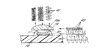
energy 40 is applied to cure the encapsulant as shown
in Fig. 6 for COB and Fig. 7 for flip chip. In Fig. 6,
the gloh top encapsulant 14 is shown in exploded view
for clarityi however, it shall be understood that the
glob top encapsulant, prior to curing with microwave
energy 40, is dispensed on top of the microelectronics
component 10 and the underlying PCB or substrate 12.
Variable frequency microwaves can rapidly and
uniformly cure the encapsulating resin for a variety of
surface mounting techniques including COB and flip
chip, without adversely affecting the IC chip,
electrical conductors, wires, or PCB encapsulated
therewithin. Single frequency microwave energy and RF
energy may be used in combination with variable
frequency microwave energy in certain applications, as
long as the selected single frequency does not cause
damage to the various components.
The use of variable frequency microwave
energy may be combined with other curing techniques
such as applying hot air to the encapsulating resin.
The present invention is advantageous over slower prior
art curing methods wherein the IC chip and PCB assembly
are typically moved to an oven and heated to high
temperatures (typically between 130~C and 170~C) from
about thirty (30) minutes up to about several hours in
some cases.
Referring now to Fig. 8A, the time to cure
various samples with variable frequency controlled
microwave energy, in accordance with the present
invention, as compared with conventional methods is
CA 022~08l7 l998-l0-07
W O 97/38441 PCT~US97/05828
-15-
tabulated. Various PCBs having various circuit
configurations thereon with IC chips mounted via flip
chip and COB were placed within a variable frequency
microwave oven. The dimensions of the PCBs were
generally about six inches by four inches (6" x 4~
Degree of cure was measured using Differential Scanning
Calorimetry (DSC) techniques, which are known to those
having skill in the art. DSC also enables the
measurement of the glass transition temperature by
measuring the change in the heat flow rate accompanying
any changes in the material. After heating with
variable frequency controlled microwave energy, the
samples were frozen until the degree of cure was
measured. As shown in Fig. 8A, the samples processed
with variable frequency controlled microwave energy, in
accordance with the present invention, reached cure in
significantly less time than comparable samples
processed with conventional heat, and at a lower
temperature. Fig. 8B illustrates the results obtained
for a variable frequency controlled microwave processed
sample at 165~C for two minutes. The temperature of
the IC chip on each PCB was monitored throughout the
cure cycle. As illustrated by the thermal profile, a
high heating rate on the IC chip occurs leading to
generally defect-free curing of the underfill
encapsulant.
Conventional curing using heat causes
stresses to build up within an IC chip, as a result of
the different coefficients of thermal expansion of the
IC chip and PCB. These stresses become locked-in upon
curing of the encapsulant. Typically, a PCB has a
higher coefficient of thermal expansion than that of an
IC chip or other microelectronics component mounted
thereto. As shown in Fig. 9, the IC chip 30, PCB 32
and encapsulant 36 are all heated to the same
temperature within conventional heat furnaces. The IC
chip temperature (Tc) and PCB temperature (Tb) are the
CA 022~0817 1998-10-07
W O 97/38441 PCT~US97/05828
-16-
same as the temperature within the furnace (Tf ) during
heating and cooling (Tc = Tb = Tf) . Conventional heat
furnaces do not have the capability to selectively heat
components or materials.
Referring now to Figs. lOA, lOB, lOC, the
build up and lock-in of stresses using conventional
heat furnaces is illustrated. The IC chip 50 has a low
coefficient of thermal expansion and the PCB 52 has a
high coefficient of thermal expansion. During heating
and cooling, the IC chip 50 and PCB 52 expand and
contract by different amounts causing stresses (Figs.
lOA, lOB). As shown in Fig. lOC, a result of this
differential expansion and contraction is that the IC
chip 50 may warp or bend. When the encapsulating resin
(not shown), either glob top or underfill, cures, this
warpage and the associated stresses are locked-in
within the IC chip 50 and substrate 52.
The use of variable frequency microwave
energy to cure an encapsulating resin helps alleviate
stresses during curing. This is because the frequency
or range(s) of frequencies can be selected so that the
encapsulant and IC chip are selectively heated without
heating the PCB to the same temperature. This is shown
in Fi~. 11, wherein the PCB 52 has a lower temperature
(Tb) during curing than either the temperature (Tc) of
the IC chip 50 or the temperature (Tu) of the
encapsulant. Because the temperature (Tb) of the PCB 52
is not as high as the temperature (Tu) of the
encapsulant and the temperature (Tc) of the IC chip 50,
the expansion and contraction of the PCB 52 is not as
great as when the entire IC chip and PCB assembly is
heated. When variable frequency microwave energy is
applied, according to the present invention, the
encapsulant temperature (Tu) is generally equivalent to
the IC chip temperature (Tc). Both the encapsulant
temperature (Tu) and the IC chip temperature (Tc) are
greater than he PCB temperature (Tb) and the
CA 022~0817 1998-10-07
W O97/38441 PCTrUS97/05828
-17-
temperature (Tf) within the furnace (Tu = Tc ~ Tb > T~).
As a result, stresses imparted upon the IC chip 50 and
interface with the PCB 52 are minimal. Upon curing of
the encapsulant 54, minimal stresses are locked into
the interface of the flip chip and IC chip 50.
The stresses generated within an IC chip
during curing can be correlated to the radius of
curvature of the IC chip after cooling has taken place.
Optical interferometry can be used to measure the
radius of curvature exhibited by an IC chip. The
radius of curvature measured on IC chips processed with
variable frequency controlled microwave energy, in
accordance with the present invention, has been
observed to be on average 918 millimeters (mm) with a
standard deviation of 25.13. This is an improvement of
50~ over similar samples processed using conventional
heating.
In addition, the cure rate of encapsulating
resin has significant effects on the properties of the
end product. Warpage of an IC chip can result from
exposure to the high temperatures required to cure the
resin. Furthermore, it is necessary to keep cure
temperatures below the reflow temperature of solder.
The use of variable frequency controlled microwave
irradiation allows the appropriate frequency or
range(s) of frequencies to be selected to rapidly cure
the encapsulating resin without causing the IC chip to
warp and without reaching the reflow temperature of
solder.
When heated via variable frequency microwave
energy, the temperature of a PCB containing IC chips is
high in the area of the IC chips and the encapsulating
resin, and low in areas not containing IC chips.
Typically, when using variable frequency microwave
energy to cure underfill encapsulating resins for flip
chip mounting, the temperature of the encapsulating
resin and IC chip may be elevated to 160~C and higher.
CA 022~0817 1998-10-07
W O 97/38441 PCT~US97/05828
-18-
The remainder of the PCB typically remains at a lower
temperature in the range of about 100~C to 140~C. Fig.
12 illustrates this. The top curve 75 represents the
temperature of an encapsulating resin during variable
frequency microwave processing. The bottom curve 77
represent the temperature of the PCB upon which an IC
chip is encapsulated via the resin. Time in seconds is
plotted along the X axis 80 and temperature in degrees
Centigrade is plotted along the Y axis 82.
The variation of the temperature of a PCB may
depend on various factors including the thickness of
the PCB, thermal conductivity of the PCB material, and
the printed circuit geometry on the PCB. The variation
of the temperature of the PCB when compared to that of
the IC chip/encapsulating resin area during a cure
process carried out at about 160~C is in the range of
about forty percent to eighty percent (40~ - 80~) of
the encapsulating resin cure temperature.
A variable frequency microwave furnace may
serve as means for sweeping resins with at least one
range of microwave frequencies to cure the resin. A
particularly preferred variable frequency microwave
furnace is described in U.S. Patent No. 5,321,222, to
Bible et al., the disclosure of which is incorporated
herein by reference in its entirety. A variable
frequency microwave furnace typically includes a
microwave signal generator or microwave voltage-
controlled oscillator for generating a low-power
microwave signal for input to the microwave furnace. A
first amplifier may be provided to amplify the
magnitude of the signal output from the microwave
signal generator or the microwave voltage-controlled
oscillator. A second amplifier is provided for
processing the signal output by the first amplifier. A
power supply is provided for operation of the second
amplifier. A directional coupler is provided for
detecting the direction of a signal and further
CA 022~0817 1998-10-07
W O 97/38441 PCTrUS97/05828
-19-
directing the signal depending on the detected
direction. Preferably a high-power broadband
amplifier, such as, but not limited to, a traveling
wave tube (TWT), tunable magnetron, tunable klystron,
tunable twystron, and a tunable gyrotron, is used to
sweep a range of frequencies of up to an octave in
bandwidth spanning the 300 MHz to 300 GHz frequency
range.
Appropriate use of variable frequency
microwave curing, as disclosed herein, enhances uniform
curing from one group of microelectronic components to
the next because placement within the microwave furnace
is not critical. By contrast, with single frequency
microwave curing, each group of encapsulated components
typically must be oriented precisely the same way to
achieve identical curing time and quality. Another
advantage of using variable frequency microwave curing,
as disclosed herein, is a reduction of the effects of
thermal stresses. By selecting frequencies that cure a
particular encapsulant without causing excessive
heating of the encapsulated component and underlying
substrate, damage from thermal stresses may be reduced
or avoided. The present invention facilitates short
curing times and selective heating of an encapsulant
without substantial heating of the PCB. Using the
present invention, materials adjacent to a surface
mounted microelectronics component having coefficients
of thermal expansion different from that of the
microelectronics component, do not have enough heat or
time to excessively expand or contract. As such,
thermal stresses do not become locked-in upon curing of
the encapsulating resin.
The practical range of frequencies within the
electromagnetic spectrum from which microwave
frequencies may be chosen is about 0.90 GHz to 40 GHz.
Every group of encapsulated components irradiated with
microwave energy typically has at least one range or
CA 022~0817 1998-10-07
W O 97/38441 PCT~US97/05828
-20-
window of frequencies, within this overall range that
will cure the encapsulant without causing damage to
other components. The term "window", as used herein,
refers to a range of microwave frequencies bounded on
one end by a specific frequency and bounded on the
opposite end by a different specific frequency. Above
or below a particular window of damage-free
frequencies, damage may occur to the encapsulated
component, substrate, or adjacent components. A window
may vary depending on component configuration,
geometry, and material composition. A window may also
vary depending on the nature and configuration of sub-
components within a component other than an IC chip
being encapsulated. Sub-components may have different
windows of damage-free frequencies, as well. An
encapsulated IC chip or component may have a sub-
component therein requiring a narrow window of
frequencies, and a sub-component therein requiring a
wide window of frequencies. The selection of a damage-
free window for a particular IC chip or component istypically obtained either empirically through trial and
error, or theoretically using power reflection curves
and the like.
Within a window of damage-free frequencies
for a particular encapsulated microelectronics
component, it is generally desirable to select the
frequencies that result in the shortest time to cure.
Preferably, a group is processed with a subset of
frequencies from the upper end of each window.
Typically, more modes can be excited with higher
frequencies than with lower frequencies which means
better uniformity in curing is typically achieved.
Additionally, more microwave energy absorption and less
microwave penetration depth, results in shorter cure
times. However, any subset of frequencies within a
window of damage-free frequencies may be used.
CA 022~0817 1998-10-07
WO97/38441 PCT~S97/05828
-21-
Many components that are irradiated with
microwave energy have multiple windows of frequencies
within which an encapsulant will cure without causing
damage to the component or underlying substrate. For
example, an encapsulated IC chip or microelectronics
component (either COB or flip chip) may be irradiated
with microwave energy without damage between 3.50 GHz
and 6.0 GHz, and may also be irradiated without damage
between 7.0 GHz and 10.0 GHz. The availability of
additional windows provides additional flexibility for
achieving rapid, yet damage-free curing. Often times,
complex geometrical configurations and material
combinations are encountered which may actually shrink
or close a particular window of frequencies available
for processing. The availability of alternative
windows permits encapsulants to be irradiated with
microwave energy without having to resort to other
curing methods.
Preferably, the step of curing is performed
by "sweeping" the encapsulant with variable frequencies
from within a particular window of damage-free
frequencies. The term "sweeping~, as used herein,
refers to irradiating the encapsulant with many of the
frequencies within a particular window. Frequency
sweeping results in uniformity of heating because many
more complementary cavity modes can be excited.
Sweeping may be accomplished by launching the different
frequencies within a window either simultaneously, or
sequentially. For example, assume the window of
damage-free frequencies for a particular encapsulated
component is 2.60 GHz to 7.0 GHz. Frequency sweeping
would involve continuously and/or selectively launching
frequencies within this range in any desirable
increments, (e.g., sweeping between 2.6 and 3.3 GHz)
such as 2.6001 GHz, 2.6002 GHz, 2.6003 GHz ... 3.30
GHz, etc. Virtually any incremental launching pattern
may be used.
CA 022~0817 1998-10-07
W O 97/38441 PCTrUS97/05828
-22-
The rate at which the different frequencies
are launched is referred to as the sweeping rate. This
rate may be any value, including, but not limited to,
milliseconds, seconds, and minutes. Preferably, the
sweep rate is as rapid as practical for a particular
resin. The uniformity in processing afforded by
frequency sweeping, provides flexibility in how
encapsulated IC chips or components are oriented within
the microwave furnace Maintaining each encapsulated
component in precisely the same orientation is not
required to achieve uniform processing.
The foregoing is illustrative of the present
invention and is not to be construed as limiting
thereof. Although a few exemplary embodiments of this
invention have been described, those skilled in the art
will readily appreciate that many modifications are
possible in the exemplary embodiments without
materially departing from the novel teachings and
advantages of this invention. Accordingly, all such
modifications are intended to be included within the
scope of this invention as defined in the claims. In
the claims, means-plus-function clause are intended to
cover the structures descri~ed herein as performing the
recited function and not only structural equivalents
but also equivalent structures. Therefore, it is to be
understood that the foregoing is illustrative of the
present invention and is not to be construed as limited
to the specific embodiments disclosed, and that
modifications to the disclosed embodiments, as well as
other embodiments, are intended to be included within
the scope of the appended claims. The invention is
defined by the following claims, with equivalents of
the claims to be included therein.