Note : Les descriptions sont présentées dans la langue officielle dans laquelle elles ont été soumises.
CA 02251504 1998-10-26
-1-
TITLE OF THE INVENTION
FEEDFORWARD AMPLIFIER WITH IMPROVED CHARACTERISTICS
WITHOUT USING PILOT SIGNAL
S
BACKGROUND OF THE INVENTION
Field of the Invention
The present invention relates to a feedforward
amplifier with linear, low distortion characteristics,
which is used for satellite communications, terrestrial
microwave communications, mobile communications and the
like.
Description of Related Art
Fig. 12 is a block diagram showing a basic
configuration of a first conventional feedforward amplifier
disclosed in Japanese patent application laid-open No. 1-
198809/1989. In Fig. 12, the reference numeral 1
designates a distortion detector, and 2 designates a
distortion eliminator. The feedforward amplifier is mainly
composed of the distortion detector 1 and distortion
eliminator 2.
In the distortion detector 1, the reference numeral 3
designates a main amplifier signal path, 4 designates a
first linear signal path, and 8 designates a directional
coupler. In the main amplifier signal path 3, the
reference numeral 9 designates a variable attenuator, 10
designates a variable phase shifter, 11 designates a main
amplifier, and 12 designates a second pilot signal
injector. In the first linear signal path 4, the reference
numeral 17 designates a delay circuit.
CA 02251504 1998-10-26
-2- -
In the distortion eliminator 2, the reference numeral 5
designates a main amplifier output path, 6 designates a
distortion injection path, and 15 designates a directional
coupler. In the main amplifier output path 5, the
reference numeral 14 designates a delay circuit, and in the
distortion injection path 6, the reference numeral 19
designates a directional coupler, 20 designates a variable
attenuator, 21 designates a variable phase shifter and 22
designates a sub-amplifier.
The reference numeral 23 designates an input terminal
of the feedforward amplifier, 24 designates an output
terminal, and 16 designates a directional coupler connected
between the distortion eliminator 2 and the output terminal
24.
The reference numeral 7 designates a first pilot signal
injector for injecting to an input path a first pilot
signal of a particular frequency, which is generated by a
signal source 25; and 26 designates a signal source for
injecting to the second pilot signal injector 12 a second
pilot signal of a particular frequency. The reference
numeral 27 designates a level detector that detects the
level of the first pilot signal by observing the output
level of the directional coupler 19 interposed in the
distortion injection path 6; and 28 designates another
level detector that detects the level of the second pilot
signal by observing the output level of the directional
coupler 16.
The reference numeral 29 designates a controller that
controls the electrically controllable variable attenuator
9 and variable phase shifter 10 such that the output level
CA 02251504 1998-10-26
-3- -
of the level detector 27 becomes minimum, and controls the
electrically controllable variable attenuator 20 and
variable phase shifter 21 such that the output level of the
level detector 28 becomes minimum.
$ Next, the operation of the first conventional
feedforward amplifier will be described.
In the distortion detector 1, the input signal applied
to the input terminal 23 and the first pilot signal of the
particular frequency, which is generated by the signal
source 25 and injected through the first pilot signal
injector 7, are delivered to the main amplifier signal path
3 and the first linear signal path 4 by the directional
coupler 8. The signal supplied to the main amplifier
signal path 3 passes through the variable attenuator 9 and
variable phase shifter 10, and is amplified by the main
amplifier 11. The signal supplied to the first linear
signal path 4 passes through the delay circuit 17 with a
delay time identical to that of the main amplifier signal
path 3.
The two signals passing through the two signal paths
are supplied through the directional couplers 13 and 18 to
the distortion injection path 6 of the distortion
eliminator 2. Thus, the directional coupler 19 in the
distortion injection path 6 and the level detector 27
detect the first pilot signal, and the controller 29
controls the variable attenuator 9 and variable phase
shifter 10 such that the output level of the level detector
27 is kept minimum. This means that the variable
attenuator 9 and variable phase shifter 10 are controlled
such that the two signals are combined in the same
CA 02251504 1998-10-26
-4-
amplitude and opposite phases in the distortion injection
path 6 of the distortion eliminator 2 through the
directional couplers 13 and 18.
Since the signal from the main amplifier signal path 3
consists of a linearly amplified signal plus nonlinear
distortion components of the main amplifier 11, and the
signal from the first linear signal path 4 consists of only
a linear signal, and the two signals are combined in the
same amplitude and opposite phases, the distortion
injection path 6 detects only the nonlinear distortion
components due to the main amplifier 11.
In the distortion eliminator 2, the signal supplied to
the main amplifier output path 5 is the sum of the linearly
amplified signal through the main amplifier 11, the
nonlinear distortion components, and the second pilot
signal of the particular frequency injected by the second
pilot signal injector 12, whereas the signal supplied to
the distortion injection path 6 is the sum of the nonlinear
distortion components of the main amplifier 11 and the
second pilot signal.
The delay amount of the delay circuit 14 is set equal
to the delay amount of the distortion injection path 6 in
advance. The directional coupler 15 combines the two
signals passing through the two paths 5 and 6, and the
directional coupler 16 and the level detector 28 detect the
level of the second pilot signal.
In this case, the controller 29 controls the variable
attenuator 20 and variable phase shifter 21 such that the
output level of the level detector 28 is kept minimum.
This means that the variable attenuator 20 and variable
CA 02251504 1998-10-26
-5-
phase shifter 21 are controlled such that the two signals
are combined by the directional coupler 15 in the same
amplitude and opposite phases. Thus, the nonlinear
distortion components added through the main amplifier
output path 5 and the nonlinear distortion components added
through the distortion injection path 6 are cancelled out
at the output terminal 24, so that only the linearly
amplified signal by the main amplifier 11 is produced from
the output terminal 24.
As a result, controlling the variable attenuators 9 and
20, and the variable phase shifters 10 and 21 makes it
possible to limit the degradation in the distortion
characteristics of the feedforward amplifier mainly due to
the characteristic changes in the main amplifier 11 and
sub-amplifier 22 by variations in temperature and a supply
voltage.
Fig. 13 is a block diagram showing a fundamental
configuration of a second conventional feedforward
amplifier disclosed in Japanese patent application laid-
open No. 5-235790/1993. The feedforward amplifier employs,
instead of the first pilot signal in the distortion
detector 1 of the first conventional feedforward amplifier,
one carrier selected from the input signal consisting a
plurality of modulation signals.
In the mobile communications, mobile stations search
for a carrier of a control channel called a perch channel,
which is sent from a base station in order to locate their
own zone and communicate with the base station that
provides a maximum receiving field. Since the base station
normally transmits at a fixed maximum transmission power
CA 02251504 1998-10-26
-6-
through the control channel, and hence its level does not
change as the carriers of other communication channels.
In Fig. 13, reference numerals 301-30n each designate a
modulator producing one of modulation signals F1-Fn
obtained by modulating carriers of different frequencies
fl-fn. Here, it is assumed that the modulation signal Fm
output from the m-th modulator 30m is assigned to the
control channel described above.
The reference numeral 31 designates a modulation signal
combiner that combines the modulation signals F1-Fn, and
supplies the combined signal to the feedforward amplifier,
in which the directional coupler 19 detects the modulation
signal Fm of the control channel, and the controller 29
controls the variable attenuator 9 and variable phase
shifter 10 such that the output level of the level detector
27 is kept minimum.
Thus, the second conventional feedforward amplifier can
achieve the same effect as the first conventional
feedforward amplifier by utilizing one of the carries in
the input signal consisting of the plurality of the
modulation signals instead of the first pilot signal in the
distortion detector 1 in the first conventional feedforward
amplifier.
Fig. 14 is a block diagram showing a basic
configuration of a third conventional feedforward amplifier
disclosed in Japanese patent application laid-open No. 4-
364602/1992.
Generally speaking, the feedforward amplifier consists
of two interference circuits for signal cancellation and
distortion cancellation, each of which can be represented
CA 02251504 1998-10-26
-7- _
by a model of a feedforward interference circuit as shown
in Fig. 14. The feedforward interference circuit
represents the distortion detector 1 or distortion
eliminator 2 in the first conventional feedforward
amplifier as shown in Fig. 12.
It comprises the directional coupler 8 for splitting
the input signal supplied through the input terminal 23
into two power signals; two signal transfer paths 53 and 54
to which the two distributed signals are supplied; and the
directional coupler 15 that combines power signals from the
signal transfer paths 53 and 54 to be output through the
output terminal 24. The signal transfer paths 53 includes
the variable attenuator 9, the variable phase shifter 10
and an amplifier 55, and the signal transfer path 54
includes the delay circuit 17 and a phase inverter 40.
Here, the amplifier 55 corresponds to the main amplifier 11
in the distortion detector 1, or to the sub-amplifier 22 in
the distortion eliminator 2.
The first pilot signal fed from the signal source 25 is
spectrum spread by a modulator 41 and is supplied to the
first pilot signal injector 7. The modulator 41 comprises
a phase modulator 43 and a band-pass filter 44. A
demodulator 42 comprises a band-pass filter 45, a local
oscillator 46, a phase modulator 47, a mixer 48 and a pilot
band-pass filter 49. In addition, a pseudorandom (PN)
generator 51 supplies the modulator 41 and demodulator 42
with PN signals, respectively, which are synchronized by a
phase modulator 52.
Next, the operation of the third conventional
feedforward amplifier will be described. The first pilot
CA 02251504 1998-10-26
_g_
signal of a single frequency from the signal source 25 is
phase modulated and spectrum spread by the phase modulator
43 using the PN code supplied from the pseudorandom (PN)
generator 51, and the spread signal is injected to the
input signal by the first pilot signal injector 7. The
output of the first pilot signal injector 7 is supplied
through the directional coupler 8 to the signal transfer
paths 53 and 54 whose outputs are combined by the
directional coupler 15. The directional coupler 16
extracts part of the output of the directional coupler 15.
The first pilot signal is demodulated by the
demodulator 42 using the output of the phase modulator 47
that phase modulates and spectrum spreads the output of the
local oscillator 46 using the PN code supplied from the
pseudorandom (PN) generator 51. The level detector 28
detects the level of the demodulated first pilot signal.
The controller 29 controls the variable attenuator 9 and
variable phase shifter 10 such that the detection level of
the first pilot signal is kept minimum.
With the foregoing arrangements, the conventional
feedforward amplifiers use pilot signals for controlling
the variable attenuator 9 or 20, and the variable phase
shifter 10 or 21 in the distortion detector 1 or distortion
eliminator 2.
The arrangements, however, have a problem of degrading
the communication quality because the detection level of
the pilot signals is minimum at the optimum operation
point, and hence the power level of the pilot signal to be
injected must be increased to heighten the detection
sensitivity. In particular., when using the pilot signal in
CA 02251504 2001-O1-12
-9-
the distortion detector 1, the distortion eliminator 2
cannot remove the first pilot signal completely, leaving
part of it in the output signal. ThLls, a new circuit must
be added to eliminate the first pilot signal, which presents
a problem of increasing the circuit scale.
SUMMARY OF THE INVENTION
The present invention is implemented to solve the
foregoing problems. It is therefore an object of the present
1.0 invention to provide a feedforward amplifier capable of
providing a high quality amplified signal with a small
circuit scale.
In accordance with one aspect of the present invention
there is provided a feedforward amplifier comprising: a
1.5 distortion detector that includes a main amplifier signal
path containing a main amplifier, and a first linear signal
path containing a first delay circuit and a directional
coupler, coupled to an output of said first delay circuit; a
distortion eliminator that includes a main amplifier output
~!0 path containing a second delay circuit, and a distortion
injection path containing a first variable attenuator, first
variable phase shifter and a sub-amplifier, and that cancels
out nonlinear distortion components, which are generated by
said main amplifier and detected by said distortion
~!5 detector, by injecting into an output. of said main amplifier
an output of said sub-amplifier which amplifies the
nonlinear distortion components; an error power extractor
for extracting output error power due to variations in said
distortion eliminator by combining in opposite phases an
..0 output signal of said distortion eliminator with a signal
CA 02251504 2001-O1-12
-10-
from said first linear signal path in said distortion
detector; a first level detector for detecting the output
error power extracted by said error power extractor; a first
controller for controlling said first variable attenuator
and said first variable phase shifter in said distortion
eliminator such that the output error power detected by said
first level detector is maintained at a minimum; wherein
said main amplifier signal path further includes a third
variable attenuator and a third variable phase shifter; and
wherein said feedforward amplifier further comprises a third
level detector for detecting, when an input signal to said
feedforward amplifier includes a control channel signal and
a main signal consisting of multiple carriers of different
frequencies, the control channel signal from said distortion
injection circuit; and a third contrc>ller for controlling
said third variable attenuator and said third variable phase
shifter in said main amplifier signal path such that the
control signal detected by said third level detector is
maintained at a minimum.
a!0 In accordance with another aspect of the present
invention there is provided a feedforward amplifier
comprising: a distortion detector that includes a main
amplifier signal path containing a main amplifier, and a
first linear signal path containing a first delay circuit
~!5 and a directional coupler, coupled tc> an output of said
first delay circuit; a distortion eliminator that includes a
main amplifier output path containing a second delay
circuit, and a distortion injection path containing a first
variable attenuator, first variable phase shifter and a sub-
_~0 amplifier, and that cancels out nonlinear distortion
CA 02251504 2001-O1-12
-11-
components, which are generated by said main amplifier and
detected by said distortion detector, by injecting into an
output of said main amplifier an output of said sub-
amplifier which amplifies the nonlinear distortion
components; an error power extractor for extracting output
error power due to variations in said distortion eliminator
by combining in opposite phases an output signal of said
distortion eliminator with a signal from said first linear
signal path in said distortion detector; a first level
detector for detecting the output error power extracted by
said error power extractor; a first controller for
controlling said first variable attenuator and said first
variable phase shifter in said distortion eliminator such
that the output error power detected by said first level
l5 detector is maintained at a minimum; wherein said main
amplifier signal path of said distortion detector further
includes a third variable attenuator and a third variable
phase shifter; and said error power extractor includes a
second linear signal path that is connected to said first
linear signal path and includes a second linear signal path
containing a second attenuator and a second variable phase
shifter; and wherein said feedforward amplifier further
comprises: a switching circuit for selecting, when using as
an input signal a CDMA modulation signal including a control
~!5 channel signal and a main signal containing multiple channel
signals, a CDMA modulation signal corresponding to the
control channel signal from one of said distortion injection
path and said error power extractor; a fourth demodulator
for demodulating the CDMA modulation signal selected by said
switching circuit; a fourth level detector for detecting the
CA 02251504 2001-O1-12
-12-
CDMA modulation signal demodulated by said fourth
demodulator; and a fourth controller for controlling, when
said switching circuit selects the CDMA modulation signal
from said error power extractor, said second variable
attenuator and said second variable phase shifter which are
interposed in said second linear signal path such that the
CDMA modulation signal detected by said fourth level
detector is kept minimum, and for controlling, when said
switching circuit selects the CDMA modulation signal from
1.0 said distortion injection path, said third variable
attenuator and said third variable phase shifter which are
interposed in said main amplifier signal path such that the
CDMA modulation signal detected by said fourth level
detector is kept minimum.
In accordance with yet another aspect of the present
invention there is provided a feedforward amplifier
comprising: a distortion detector that includes a main
amplifier signal path containing a main amplifier, and a
first linear signal path containing a first delay circuit
~'.0 and a directional coupler, coupled to an output of said
first delay circuit; a distortion eliminator that includes a
main amplifier output path containing a second delay
circuit, and a distortion injection path containing a first
variable attenuator, first variable phase shifter and a sub-
~'.5 amplifier, and that cancels out nonlinear distortion
components, which are generated by said main amplifier and
detected by said distortion detector, by injecting into an
output of said main amplifier an output of said sub-
amplifier which amplifies the nonlinear distortion
;SO components; an error power extractor for extracting output
CA 02251504 2001-O1-12
-13-
error power due to variations in said distortion eliminator
by combining in opposite phases an output signal of said
distortion eliminator with a signal from said first linear
signal path in said distortion detector; a first level
detector for detecting the output error power extracted by
said error power extractor; a first controller for
controlling said first variable attenuator and said first
variable phase shifter in said distortion eliminator such
that the output error power detected by said first level
l0 detector is maintained at a minimum; and wherein said error
power extractor comprises a second linear signal path that
includes a second variable attenuator and a second variable
phase shifter and is connected to said first linear signal
path, and extracts, when an input signal to said feedforward
amplifier includes a control channel signal and a main
signal consisting of multiple carriers of different
frequencies, the control channel signal, and wherein said
feedforward amplifier further comprises a second level
detector for detecting the control channel signal extracted
by said error power extractor; and a second controller for
controlling said second variable attenuator and said second
variable phase shifter in said error power extractor such
that the control channel signal detected by said second
level detector is maintained at a minimum; wherein said main
~!5 amplifier signal path in said distortion detector further
includes a third variable attenuator; and said first linear
signal path in said distortion detector further includes a
fourth variable attenuator and a fourth variable phase
shifter; and wherein said feedforward amplifier further
..0 comprises: a fifth level detector for detecting said
CA 02251504 2001-O1-12
-14-
control channel signal from said distortion injection path;
a fifth controller for controlling said fourth variable
attenuator and said fourth variable phase shifter which are
interposed in said first linear signal path such that the
control channel signal detected by said fifth level detector
is maintained at a minimum; a sixth level detector for
detecting an output signal of said distortion eliminator;
and a sixth controller for controlling said third variable
attenuator which is interposed in said main amplifier signal
path such that the output signal detected by said sixth
level detector is maintained at a fixed value.
BRIEF DESCRIPTION OF THE DRAWINGS
Fig. 1 is a block diagram showing an embodiment 1 of a
l5 feedforward amplifier in accordance with the present
invention;
Fig. 2 is a block diagram showing an embodiment 2 of
the feedforward amplifier in accordance with the present
invention;
Fig. 3 is a block diagram showing an embodiment 3 of
the feedforward amplifier in accordance with the present
invention;
Fig. 4 is a block diagram showing an embodiment 4 of
the feedforward amplifier in accordance with the present
a!5 invention;
Fig. 5 is a block diagram showing an embodiment 5 of
the feedforward amplifier in accordance with the present
invention;
CA 02251504 1998-10-26
-15
Fig. 6 is a block diagram showing an embodiment 6 of
the feedforward amplifier in accordance with the present
invention;
Fig. 7 is a block diagram showing an embodiment 7 of
the feedforward amplifier in accordance with the present
invention;
Fig. 8 is a block diagram showing an embodiment 8 of
the feedforward amplifier in accordance with the present
invention;
Fig. 9 is a block diagram showing an embodiment 9 of
the feedforward amplifier in accordance with the present
invention;
Fig. 10 is a block diagram showing an embodiment 10 of
the feedforward amplifier in accordance with the present
invention;
Fig. 11 is a block diagram showing an embodiment 11 of
the feedforward amplifier in accordance with the present
invention;
Fig. 12 is a block diagram showing a basic
configuration of a first conventional feedforward
amplifier;
Fig. 13 is a block diagram showing a basic
configuration of a second conventional feedforward
amplifier; and
Fig. 14 is a block diagram showing a basic
configuration of a third conventional feedforward
amplifier.
DETAILED DESCRIPTION OF THE PREFERRED EMBODIMENTS
The invention will now be described with reference to
CA 02251504 1998-10-26
-16-
the accompanying drawings.
EMBODIMENT 1
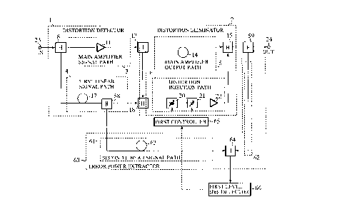
Fig. 1 is a block diagram showing a configuration of an
embodiment 1 of a feedforward amplifier in accordance with
the present invention. In Fig. 1, the reference numeral 1
designates a distortion detector, 2 designates a distortion
eliminator, and 60 designates an error power extractor.
The feedforward amplifier is mainly composed of the
distortion detector 1, distortion eliminator 2 and error
power extractor 60.
In the distortion detector 1, the reference numeral 8
designates a directional coupler, 3 designates a main
amplifier signal path, and 4 designates a first linear
signal path, in which the main amplifier signal path 3
consists of the main amplifier 11 and the first linear
signal path 4 consists of the delay circuit 17 and a
directional coupler 58.
In the distortion eliminator 2, the reference numeral 5
designates a main amplifier output path, 6 designates a
distortion injection path, and 15 designates a directional
coupler for injecting the output signal of the distortion
injection path 6 into the output signal of the main
amplifier output path 5. The reference numerals 13 and 18
each designate a directional coupler interposed between the
distortion detector 1 and distortion eliminator 2. The
main amplifier output path 5 consists of the delay circuit
14, and the distortion injection path 6 consists of the
first variable attenuator 20, first variable phase shifter
21 and sub-amplifier 22.
In the error power extractor 60, the reference numeral
CA 02251504 1998-10-26
-17-
61 designates a second linear signal path, 62 designates an
output reference path, and 64 designates a directional
coupler for combining the output of the second linear
signal path 61 with that of the output reference path 62 in
the same amplitude and opposite phases. The second linear
signal path 61 consists of a delay circuit 63.
The reference numeral 66 designates a first level (Pe)
detector for detecting the combined output from the
directional coupler 64, and 65 designates a first
controller for controlling the electrically controllable
first variable attenuator 20 and first variable phase
shifter 21 such that the detection value output from the
first level (Pe) detector 66 is kept minimum.
The reference numeral 23 designates an input terminal
of the feedforward amplifier, 24 designates an output
terminal, and 59 designates a directional coupler connected
between the distortion eliminator 2 and the output terminal
24.
Next, the operation of the present embodiment 1 will be
described.
In the distortion detector 1, the input signal applied
to the input terminal 23 is delivered to the main amplifier
signal path 3 and first linear signal path 4 through the
directional coupler 8. The signal supplied to the main
amplifier signal path 3 is amplified by the main amplifier
11. The signal supplied to the first linear signal path 4
passes through the delay circuit 17 with the same delay
time as that of the main amplifier signal path 3.
The two signals passing through the two signal paths
are combined through the directional couplers 13 and 18 in
CA 02251504 1998-10-26
_18_ _
the same amplitude and opposite phases, and supplied to the
distortion injection path 6 of the distortion eliminator 2.
Since the signal from the main amplifier signal path 3
consists of a linearly amplified signal plus nonlinear
distortion components of the main amplifier 11, and the
signal from the first linear signal path 4 consists of only
a linear signal, and the two signals are combined in the
same amplitude and opposite phases, the distortion
injection path 6 detects only the nonlinear distortion
components added by the main amplifier 11.
In the distortion eliminator 2, the signal supplied to
the main amplifier output path 5 is the signal amplified by
the main amplifier 11, whereas the signal supplied to the
distortion injection path 6 is the nonlinear distortion
components of the main amplifier 11.
The delay amount of the delay circuit 14 is set equal
to the delay amount of the distortion injection path 6 in
advance. The values of the first variable attenuator 20
and first variable phase shifter 21 are initially set such
that the directional coupler 15 combines the two signals
passing through the two paths 5 and 6 in the same amplitude
and opposite phases.
In this initial state, the delay amount of the delay
circuit 63 in the error power extractor 60 is set equal to
that of the distortion injection path 6, and the output of
the output reference path 62 is combined with that of the
second linear signal path 61 by the directional coupler 64
in the same amplitude and opposite phases. The combined
power (Pe) is supplied to the first level (Pe) detector 66,
and the first controller 65 controls the first variable
CA 02251504 1998-10-26
-19-
attenuator 20 and first variable phase shifter 21 such that
the detection value of the first level (Pe) detector 66 is
maintained at a minimum.
According to the present embodiment 1, since the pilot
S signals are removed, the signal sources for generating the
pilot signals can be obviated, which serves to reduce the
size of the device.
Furthermore, the distortion characteristics of the
feedforward amplifier can be maintained at the initial
state level against the changes in the characteristics of
the sub-amplifier 22 due to the variations in the
temperature, supply voltage and the like. In other words,
the present embodiment 1 can maintain the feedforward
amplifier at its optimum distortion state.
EMBODIMENT 2
Fig. 2 is a block diagram showing a configuration of an
embodiment 2 of the feedforward amplifier in accordance
with the present invention, in which the second linear
signal path 61 in the error power extractor 60 includes a
second variable attenuator 69 and a second variable phase
shifter 70 besides the delay circuit 63.
The reference numeral 67 designates a second level (Vc)
detector that detects, when the input signal is composed of
a control channel signal (Vc) and a main signal (Vs)
consisting of multiple carriers of different frequencies,
the control channel signal (Vc) included in the combined
output from the directional coupler 64; and 68 designates a
second controller for controlling the electrically
controllable second variable attenuator 69 and second
CA 02251504 1998-10-26
-20- -
variable phase shifter 70 such that the detection value of
the second level (Vc) detector 67 is kept minimum. Since
the remaining configuration is the same as that of the
embodiment 1, the duplicate description is avoided here.
Next, the operation of the present embodiment 2 will be
described.
In the present embodiment 2, it is assumed that the
input signal includes the control channel signal (Vc) and
the main signal (Vs) consisting of the multiple carriers of
different frequencies. Thus, the second level (Vc)
detector 67 detects the control channel signal (Vs)
contained in the combined output from the directional
coupler 64 in the error power extractor 60. Then, the
second controller 68 controls the second variable
attenuator 69 and second variable phase shifter 70 such
that the detection output of the second level (Vc) detector
67 is maintained at a minimum.
According to the present embodiment 2, the directional
coupler 64 can always combine the output of the output
reference path 62 with that of the second linear signal
path 61 in the same amplitude and opposite phases, and
hence the accuracy of the first level (Pe) detector 66 can
be maintained at a fixed value independently of the
amplitude and phase errors due to the variations in
characteristics of the output reference path 62 and second
linear signal path 61 in the error power extractor 60.
This makes possible maintaining the distortion
characteristics of the feedforward amplifier at an optimum
state. The other advantages are similar to those of the
foregoing embodiment 1.
CA 02251504 1998-10-26
-21-
EMBODIMENT 3
Fig. 3 is a block diagram showing a configuration of an
embodiment 3 of the feedforward amplifier in accordance
with the present invention, in which the main amplifier
signal path 3 in the distortion detector 1 includes a third
variable attenuator 9 and a third variable phase shifter
10, and the distortion injection path 6 in the distortion
eliminator 2 comprises a directional coupler 57.
In addition, the reference numeral 71 designates a
third level (Vc) detector for detecting, when the input
signal is employed which includes the control channel
signal (Vc) and the main signal (Vs) consisting of the
multiple carriers of different frequencies, the control
channel signal contained in a signal extracted by the
directional coupler 57; and 72 designates a third
controller for controlling the electrically controllable
third variable attenuator 9 and third variable phase
shifter 10 such that the detection value of the third level
(Vc) detector 71 is maintained at a minimum.
Since the remaining configuration is the same as that
of the foregoing embodiment 1, the duplicate description is
avoided here.
Next, the operation of the present embodiment 3 will be
described.
In the present embodiment 3, the input signal includes
the control channel signal (Vc) and the main signal (Vs)
consisting of the multiple carriers of different
frequencies, and the directional coupler 57 extract part of
the input signal. The third level (Vc) detector 71 detects
the control channel signal (Vs) contained in the signal
CA 02251504 1998-10-26
-22-
extracted by the directional coupler 57. Then, the third
controller 72 controls the third variable attenuator 9 and
third variable phase shifter 10 such that the detection
value of the third level (Vc) detector 71 is maintained at
S a minimum.
Thus, the present embodiment 3 can always combine the
output of the main amplifier signal path 3 with that of the
first linear signal path 4 in the same amplitude and
opposite phases before they are supplied to the distortion
injection path 6 in the distortion eliminator 2. The other
advantages are similar to those of the foregoing embodiment
1.
EMBODIMENT 4
Fig. 4 is a block diagram showing a configuration of an
embodiment 4 of the feedforward amplifier in accordance
with the present invention, which is a combination of the
arrangements of the embodiments 2 and 3. More
specifically, the second level (Vc) detector 67, second
controller 68, second variable attenuator 69 and second
variable phase shifter 70 of the embodiment 2 is combined
with the directional coupler 57, third level (Vc) detector
71, third controller 72, third variable attenuator 9 and
third variable phase shifter 10 of the embodiment 3. Since
the remaining configuration is the same as that of the
embodiment 1, the duplicate description is avoided here.
According to the present embodiment 4, the directional
coupler 64 can always combine the output of the output
reference path 62 with that of the second linear signal
path 61 in the same amplitude and opposite phases, and
CA 02251504 1998-10-26
-23-
hence the accuracy of the first level (Pe) detector 66 can
be maintained at a fixed value independently of the
amplitude and phase errors due to the variations in
characteristics of the output reference path 62 and second
linear signal path 61 in the error power extractor 60.
This makes possible maintaining the distortion
characteristics of the feedforward amplifier at an optimum
state.
In addition, the output of the main amplifier signal
path 3 can be always combined with that of the first linear
signal path 4 in the same amplitude and opposite phases
before they are supplied to the distortion injection path 6
in the distortion eliminator 2.
The other advantages are similar to those of the
foregoing embodiment 1.
EMBODIMENT 5
Fig. 5 is a block diagram showing a configuration of an
embodiment 5 of the feedforward amplifier in accordance
with the present invention. In Fig. 5, the reference
numeral 73 designates a first demodulator that is provided
when a CDMA (code division multiple access) modulation
signal, which includes the control channel signal (Vc) and
the main signal (Vs) consisting of multiple channel
signals, is used as the input signal, and that demodulates
a part of the CDMA modulation signal which is extracted by
the directional coupler 57 in the distortion injection path
6 and corresponds to the control channel signal (Vc).
Since the remaining configuration is the same as that of
the embodiment 3, the duplicate description thereof is
CA 02251504 1998-10-26
-24-
avoided here.
Next, the operation of the present embodiment 5 will be
described.
In the present embodiment 5, the first demodulator 73
demodulates the CDMA modulation signal corresponding to the
control channel signal (Vc), when the CDMA modulation
signal, which includes the control channel signal (Vc) and
the main signal (Vs) consisting of the multiple channel
signals, is used as the input signal. Subsequently, the
third level (Vc) detector 71 detects the level of the
demodulated CDMA modulation signal, and the third
controller 72 controls the third variable attenuator 9 and
third variable phase shifter 10 such that the detection
value of the third level (Vc) detector 71 is kept minimum.
According to the present embodiment 5, applying the
CDMA modulation signal corresponding to the control channel
signal (Vc) can make the feedforward amplifier
insusceptible to interference such as noise, and heighten
the detection sensitivity of the control channel signal
(Vc). The other advantages are similar to those of the
foregoing embodiment 3.
EMBODIMENT 6
Fig. 6 is a block diagram showing a configuration of an
embodiment 6 of the feedforward amplifier in accordance
with the present invention. In Fig. 6, the reference
numeral 74 designates a second demodulator that is provided
when the CDMA modulation signal, which includes the control
channel signal (Vc) and the main signal (Vs) consisting of
multiple channel signals, is used as the input signal, and
CA 02251504 1998-10-26
-25-
that demodulates the combined output of the directional
coupler 64 in the error power extractor 60. Since the
remaining configuration is the same as that of the
embodiment 4 plus the first demodulator 73, the duplicate
description thereof is avoided here.
Next, the operation of the present embodiment 6 will be
described.
In the present embodiment 6, the second demodulator 74
demodulates the CDMA modulation signal corresponding to the
control channel signal (Vc), when the CDMA modulation
signal, which includes the control channel signal (Vc) and
the main signal (Vs) consisting of the multiple channel
signals, is used as the input signal. Subsequently, the
second level (Vc) detector 67 detects the level of the
demodulated CDMA modulation signal, and the second
controller 68 controls the second variable attenuator 69
and second variable phase shifter 70 such that the output
value of the second level (Vc) detector 67 is kept minimum.
According to the present embodiment 6, applying the
CDMA modulation signal corresponding to the control channel
signal (Vc) can make the feedforward amplifier
insusceptible to interference such as noise, and heighten
the detection sensitivity of the control channel signal
(Vc). The other advantages are similar to those of the
foregoing embodiment 4.
EMBODIMENT 7
Fig. 7 is a block diagram showing a configuration of an
embodiment 7 of the feedforward amplifier in accordance
with the present invention.. In Fig. 7, the reference
CA 02251504 1998-10-26
-26-
numeral 75 designates a switching circuit that is provided
when the CDMA modulation signal, which includes the control
channel signal (Vc) and the main signal (Vs) consisting of
multiple channel signals, is used as the input signal, and
S that temporally selects one of the CDMA modulation signals
included in the combined output from the directional
coupler 64 and in the signal extracted by the directional
coupler 57.
The reference numeral 76 designates a fourth
demodulator for demodulating the CDMA modulation signal
corresponding to the control channel signal (Vc) selected
by the switching circuit 75; and 77 designates a fourth
level (Vc) detector for detecting the CDMA modulation
signal demodulated by the fourth demodulator 76.
The reference numeral 78 designates a fourth controller
that controls, when the switching circuit 75 selects the
CDMA modulation signal output from the directional coupler
64, the second variable attenuator 69 and second variable
phase shifter 70 such that the detection value of the
fourth level (Vc) detector 77 is kept minimum, and that
controls, when the switching circuit 75 selects the CDMA
modulation signal output from the directional coupler 57,
the third variable attenuator 9 and third variable phase
shifter 10 such that the detection value of the fourth
level (Vc) detector 77 is kept minimum. Since the
remaining configuration is analogous to the configurations
of the embodiments 5 and 6, the duplicate description
thereof is avoided here.
Next, the operation of the present embodiment 7 will be
described.
CA 02251504 1998-10-26
-27-
In the present embodiment 7, the fourth demodulator 76
demodulates the CDMA modulation signal corresponding to the
control channel signal (Vc) supplied from the directional
coupler 57 or 64 through the switching circuit 75.
Subsequently, the fourth level (Vc) detector 77 detects the
level of the demodulated CDMA modulation signal. Then, the
fourth controller 78 controls, when the switching circuit
75 connects the output of the directional coupler 64 with
the fourth demodulator 76, the second variable attenuator
69 and second variable phase shifter 70 such that the
detection value of the fourth level (Vc) detector 77 is
maintained at a minimum, and controls, when the switching
circuit 75 connects the output of the directional coupler
57 with the fourth demodulator 76, the third variable
attenuator 9 and third variable phase shifter 10 such that
the detection value of the fourth level (Vc) detector 77 is
maintained at a minimum.
According to the present embodiment 7, the output of
the main amplifier signal path 3 can be combined with the
output of the first linear signal path 4 in the same
amplitude and opposite phases before they are supplied to
the distortion injection path 6 in the distortion
eliminator 2. Likewise, the output of the output reference
path 62 can be combined with the output of the second
linear signal path 61 by the directional coupler 64 in the
same amplitude and opposite phases.
In addition, the accuracy of the first level (Pe)
detector 66 can be maintained at a fixed value
independently of the amplitude and phase errors due to the
variations in characteristics of the output reference path
CA 02251504 1998-10-26
-28-
62 and second linear signal path 61 in the error power
extractor 60. This makes possible maintaining the
distortion characteristics of the feedforward amplifier at
an optimum state.
Moreover, using the switching circuit 75 enables the
first demodulator 73 and second demodulator 74, the third
level (Vc) detector 71 and second level (Vc) detector 67,
and the third controller 72 and second controller 68, each
pair of which is provided separately in the foregoing
embodiment 6, to be incorporated into the fourth
demodulator 76, fourth level (Vc) detector 77 and fourth
controller 78, respectively, in the present embodiment 7.
This can reduce the size of the device. The remaining
advantages are similar to those of the embodiment 1.
EMBODIMENT 8
Fig. 8 is a block diagram showing a configuration of an
embodiment 8 of the feedforward amplifier in accordance
with the present invention, in which the first linear
signal path 4 includes a fourth variable attenuator 80 and
a fourth variable phase shifter 81. The reference numeral
82 designates a fifth level (Pt) detector for detecting,
when the control channel signal (Vc) and the main signal
consisting of the multiple carriers of different
frequencies are used as the input signal, the control
channel signal (Vc) contained in the signal extracted by
the directional coupler 57; and 83 designates a fifth
controller for controlling the electrically controllable
fourth variable attenuator 80 and fourth variable phase
shifter 81 such that the detection level of the fifth level
CA 02251504 1998-10-26
-29-
(Pt) detector 82 is maintained at a minimum.
The reference numeral 84 designates a directional
coupler provided between the distortion eliminator 2 and
the output terminal 24; 85 designates a sixth level (Pout)
detector for detecting from the directional coupler 84 the
output power (Pout) of the feedforward amplifier; and 86
designates a sixth controller for controlling the third
variable attenuator 9 provided in the main amplifier signal
path 3 of the distortion detector 1 such that the detection
value of the sixth level (Pout) detector 85 is maintained
at a fixed value. Since remaining configuration is the
same as that of Fig. 2, the duplicate description thereof
is omitted here.
Next, the operation of the present embodiment 8 will be
described.
In the present embodiment 8, the directional coupler 57
extracts part of the input signal containing the control
channel signal (Vc) and the main signal consisting of the
multiple carriers of different frequencies, and the fifth
level (Pt) detector 82 detects the control channel signal
(Vc) included in that extracted signal. Then, the fifth
controller 83 controls the fourth variable attenuator 80
and fourth variable phase shifter 81 such that the
detection level of the fifth level (Pt) detector 82 is
maintained at a minimum.
Furthermore, the sixth level (Pout) detector 85 detects
the output power (Pout) of the feedforward amplifier fed
from the directional coupler 84 immediately previous to the
output terminal 24, and the sixth controller 86 controls
the third variable attenuator 9 interposed in the main
CA 02251504 1998-10-26
-30-
amplifier signal path 3 of the distortion detector 1 such
that the detection level of the sixth level (Pout) detector
85 is maintained at a fixed value.
According to the present embodiment 8, the output of
the main amplifier signal path 3 can be always combined
with the output of the first linear signal path 4 in the
same amplitude and opposite phases before they are supplied
to the distortion injection path 6 of the distortion
eliminator 2. In addition, the output power of the
feedforward amplifier can be maintained at a fixed level by
keeping the detection value of the sixth level (Pout)
detector 85 at a fixed level. The other advantages are
similar to those of the embodiment 2.
EMBODIMENT 9
Fig. 9 is a block diagram showing a configuration of an
embodiment 9 of the feedforward amplifier in accordance
with the present invention, which comprises the second
demodulator 74 as shown in the embodiment 6 in addition to
the configuration of the embodiment 8.
Next, the operation of the present embodiment 9 will be
described.
In the present embodiment 9, the second demodulator 74
demodulates the CDMA modulation signal corresponding to the
control channel signal (Vc), when the CDMA modulation
signal, which includes the control channel signal (Vc) and
the main signal (Vs) consisting of the multiple channel
signals, is used as the input signal. Thus, the second
level (Vc) detector 67 detects the level of the demodulated
CDMA modulation signal, and-the second controller 68
CA 02251504 1998-10-26
-31-
controls the second variable attenuator 69 and second
variable phase shifter 70 such that the output value of the
second level (Vc) detector 67 is kept minimum.
According to the present embodiment 9, applying the
CDMA modulation signal corresponding to the control channel
signal (Vc) can make the feedforward amplifier
insusceptible to interference such as noise, and heighten
the detection sensitivity of the control channel signal
(Vc). The other advantages are similar to those of the
foregoing embodiment 8.
EMBODIMENT 10
Fig. 10 is a block diagram showing a configuration of
an embodiment 10 of the feedforward amplifier in accordance
with the present invention, in which the reference numeral
90 designates a first linearizer that is provided in the
main amplifier signal path 3 in the distortion detector 1
to compensates for the distortion characteristics of the
main amplifier 11. Since the remaining configuration is
the same as that of the embodiment 1, the duplicate
description is avoided here.
Next, the operation of the present embodiment 10 will
be described.
In the present embodiment 10, the signal which is
supplied to the main amplifier signal path 3 in the
distortion detector 1 passes through the first linearizer
90, and is amplified by the main amplifier 11. In the
course of this, the distortion characteristics of the main
amplifier 11 are compensated by the first linearizer 90
because of the amplitude and phase characteristics of the
CA 02251504 1998-10-26
-32-
first linearizer 90 reversal to those of the main amplifier
11.
According to the present embodiment 10, the distortion
characteristics of the main amplifier 11 can be compensated
by the first linearizer 90. This enables the distortion,
characteristics of the feedforward amplifier to be
improved. The other advantages are similar to those of the
embodiment 1.
EMBODIMENT 11
Fig. 11 is a block diagram showing a configuration of
an embodiment 11 of the feedforward amplifier in accordance
with the present invention, in which the reference numeral
91 designates a second linearizer that is provided in the
distortion injection path 6 of the distortion eliminator 2
to compensate for the distortion characteristics of the
sub-amplifier 22. Since the remaining configuration is the
same as that of the embodiment 10, the duplicate
description is avoided here.
Next, the operation of the present embodiment 11 will
be described.
In the present embodiment 11, the signal which is
supplied to the distortion injection path 6 in the
distortion eliminator 2 passes through the second
linearizer 91, and is amplified by the sub-amplifier 22.
In the course of this, the distortion characteristics of
the sub-amplifier 22 are compensated by the second
linearizer 91 because of the amplitude and phase
characteristics of the second linearizer 91 reversal to
those of the sub-amplifier 22.
CA 02251504 1998-10-26
-33-
According to the present embodiment 11, the distortion
characteristics of the sub-amplifier 22 can be compensated
by the second linearizer 91. This enables the distortion
characteristics of the feedforward amplifier to be
improved. The other advantages are similar to those of the
embodiment 2.