Note : Les descriptions sont présentées dans la langue officielle dans laquelle elles ont été soumises.
CA 02252875 2001-12-28
SEMICONDUCTOR DEVICE AND FABRICATION METHOD THEREOF
BACKGROUND OF THE INVEl''TION
1. Field of the Tnvention
The present invention relates to a gallium-arsenide integrated circuit for use
in a
micro wave circuit and, particularly, to a technique for integrating a large
capacitor formed
of high dielectric constant material and a small capacitor formed of a
dielectric material
having relatively low dielectric constant.
2. Description of Related Art
In a gallium-arsenide (GaAs) integrated circuit for use in a micro wave
circuit, a field
effect transistor (FET), a large capacitor used for a power source or used as
a coupling
capacitor and a small capacitor necessary in matching circuits have been
integrated. As a
dielectric material between electrodes of a large capacitor, a thin film of
SrTi03(STO),
BaTiO~, [BaXSrI_,;]TiO~(BST), PbTi03 or [PbZr]Ti03(PZT), etc., whose relative
dielectric
constant is 100 or more is used. SiNX having relative dielectric constant as
low as about 7 is
used as a dielectric material betu-een electrodes of a small capacitor.
Japanese Patent Application Laid-open No. Hei 6-120425 discloses an
integration of
FET and capacitors. According to the disclosed technique, the FET is formed
first and,
then, the large capacitor is formed by using high dielectric constant
material.
However, since, in the disclosed technique, the FET and the capacitor are
formed
~0 separately, the number of manufacturing steps is increased. Further, in
order to form the
CA 02252875 2001-12-28
-2-
capacitor having different capacity, other manufacturing steps are required.
SUMMARY OF THE INVENTION
An object of the present invention is to provide a semiconductor device which
is an
integrated circuit including capacitors having substantially different
capacitances and a
manufacturing method for manufacturing the semiconductor device with a smaller
number of
manufacturing steps.
According to a first aspect of the present invention, an upper electrode of a
capacitor
having small capacitance (referred to as "small capacitor", hereinafter) and a
lower electrode of
a capacitor having large capacitance (referred to as "large capacitor",
hereinafter) are formed
simultaneously. That is, after a film of low dielectric constant material is
formed on a lower
electrode of the small capacitor, the upper electrode of the small capacitor
and the lower
electrode of the large capacitor are formed simultaneously and a film of high
dielectric constant
material and the upper electrode are laminated on the lower electrode of the
large capacitor.
Thus, a semiconductor device in which the upper electrode of the small
capacitor and the lower
electrode of the large capacitor are formed as different regions of the same
conductive film. It
is enough that dielectric constant of the film of low dielectric constant
material is lower than
dielectric constant of the film of high dielectric constant material formed on
the lower electrode
of the large capacitor. The conductive film may be of a metal material or a
conductive oxide
material.
According to a further aspect of the present invention, there is provided a
method for
manufacturing a semiconductor device having a first capacitor having a small
capacitance and
a second capacitor having a large capacitance , the first and second
capacitors being formed on
a single substrate, comprising the steps of forming a first dielectric film
having a low dielectric
CA 02252875 2001-12-28
-2a-
constant on a lower electrode of said first capacitor and simultaneously
forming an upper
electrode of said first capacitor and a lower electrode of said second
capacitor on said first
dielectric film; and forming a second dielectric film having a high dielectric
constant on said
lower electrode of said second capacitor and forming an upper electrode of
said second capacitor
on said second dielectric film.
According to another aspect of the present invention, there is provided a
semiconductor
device comprising a first capacitor having a small capacitance and a second
capacitor having a
large capacitance, said first and second capacitors being formed on a single
substrate, wherein
an upper electrode of said first capacitor and a lower electrode of said
second capacitor are
formed on different regions of a conductive film.
It is preferable to form active elements on a substrate and form the lower
electrode of the
small capacitor simultaneously with the formation of electrodes of the active
elements.
In detail, at the time of formation of the electrode, for example, a gate
electrode of the
CA 02252875 1998-11-OS
3
active element, the metal film is left on a portion of the substrate. The
active element and
the metal film are covered by an inter-layer film. An opening is formed in the
inter-layer
film such that a portion of the metal film is exposed. On the wafer, a
dielectric film of a
dielectric material having low dielectric constant (referred to as "low
dielectric constant
film", hereinafter), a first conductive film, a dielectric film of a
dielectric material having
high dielectric constant (referred to as "high dielectric constant film",
hereinafter) and a
second conductive film are formed in the order. The large capacitor is formed
by processing
the second conductive film, the high dielectric constant film and the first
conductive film
and the small capacitor is formed by removing the second conductive film and
the high
dielectric constant film correspondingly to the position of the metal film and
processing the
first conductive film.
According to a second aspect of the present invention, the dielectric material
between the electrodes of the small capacitor has a double layer structure
composed of a
high dielectric constant film and a low dielectric constant film, the low
dielectric constant
film of the large capacitor is removed and the lower electrodes of the small
and large
capacitors are formed simultaneously and the upper electrodes of the small and
large
capacitor are formed simultaneously. That is, the lower electrode of the small
capacitor and
the lower electrode of the large capacitor are formed simultaneously and the
high dielectric
constant film and the low dielectric film are formed on these lower electrodes
in the order.
The low dielectric constant film in a region in which the large capacitor is
to be formed is
removed and the upper electrodes of the small and large capacitors are
simultaneously
formed on the low dielectric constant film in a region in which the small
capacitor is to be
formed and on the high dielectric constant film in the region in which the
large capacitor is
CA 02252875 2001-12-28
-4-
to be formed. Thus, the semiconductor device including the small and large
capacitors having
the simultaneously formed lower electrodes, the high dielectric constant film
simultaneously
formed as the inter-electrode dielectric layer, the low dielectric constant
film formed in the inter-
electrode layer of only the small capacitor and the upper electrodes formed
simultaneously as the
same conductive film.
According to another aspect of the present invention, there is provided a
method for
manufacturing a semiconductor device having a first capacitor having a small
capacitance and
a second capacitor having a large capacitance, the first and second capacitors
being formed on
a single substrate, comprising the steps of forming lower electrodes of said
second capacitor and
said first capacitor; forming a first dielectric film having a low dielectric
constant and a second
dielectric film having a high dielectric constant on said lower electrodes;
removing said first
dielectric film from a region in which said second capacitor is to be formed;
and simultaneously
forming upper electrodes on said first dielectric film in a region in which
said first capacitor is
to be formed and on said second dielectric film in the region in which said
second capacitor is
to be formed, respectively.
It is preferable to form at least one active element and to form the lower
electrodes of
the small and large capacitors simultaneously with a formation of an electrode
of the active
element.
In detail, the active element is formed on the substrate, a metal film used to
form the
electrode ofthe active element is left on at least two portions of said
substrate, the active element
and the metal film are covered by an inter-layer film, openings are formed in
the two regions of
the inter-layer film to expose portions of the metal film, a second dielectric
film having a high
dielectric constant and a first dielectric film having a low dielectric
constant are laminated, the
CA 02252875 2001-12-28
-4a-
first dielectric film is removed from one of the two regions, in which the
large capacitor is to be
formed, and the small capacitor and the large capacitors are formed in the
region in which the
low dielectric constant film exists and the large capacitor is formed in the
region from which the
low dielectric constant film is removed, by processing the conductive film.
According to a still further aspect of the present invention, there is
provided a
semiconductor device comprising a first capacitor having a small capacitance
and a second
capacitor having a large capacitance, said first capacitor and said second
capacitor being formed
on a single substrate, wherein lower electrodes of said first and second
capacitors are formed on
different regions of a conductive film; said first and second capacitors have
a high dielectric
constant film formed simultaneously as an inter-electrode dielectric layer;
said inter-electrode
dielectric layer of said first capacitor also includes a low dielectric
constant film; and upper
electrodes of said first and second capacitors are formed by a conductive film
of the same
material.
BRIEF DESCRIPTION OF THE DRAWLNGS
The above and other objects, features and advantages of the present invention
will
become more apparent by reference to the following detailed description of the
invention taken
in conjunction with the accompanying drawings, in which:
Figs. 1 a to I a are cross sections of a semiconductor device, showing
manufacturing
CA 02252875 1998-11-OS
steps according to a first embodiment of the present invention;
Figs. 2a and 2b are cross sections of a semiconductor device, showing
manufacturing
steps according to a second embodiment; and
Figs. 3a to 3e are cross sections of a semiconductor device, showing
manufacturing
5 steps according to a third embodiment of the present invention.
DETAILED DESCRIPTION OF THE PREFERRED EMBODIMENTS
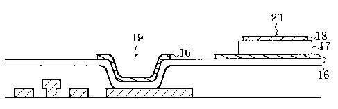
Figs. la to 1e are cross sections of a semiconductor device composed of a GaAs
substrate and an FET, a small capacitor and a large capacitor formed on the
substrate,
showing manufacturing steps according to a first embodiment of the present
invention.
According to the first embodiment of the present invention, the FET 12 having
a gate
electrode 12a and an ohmic electrode 12b is formed on the GaAs substrate 11
and, in
forming the gate electrode 12a of the FET 12, a metal film 13 is left on a
portion of the
GaAs substrate 11, as shown in Fig. la. In this embodiment, the gate electrode
12a and the
metal film 13 are sputtered Au/WSi films.
Then, as shown in Fig. 1b, the FET 12 and the metal film 13 are covered by a
Si02
inter-layer film 14, an opening is formed in the Si02 inter-layer film 14 to
expose a portion
of the metal film 13 and a low dielectric constant film 15 is formed on the
whole wafer. In
this embodiment, the low dielectric constant film 15 is a SiNX film formed by
plasma CVD.
Then, as shown in Fig. 1 c, a first conductive film 16, a high dielectric
constant film
17 and a second conductive film 18 are formed in lamination. The first
conductive film 16
has a double layer structure having an upper Ti layer portion 20 nm thick and
a lower Pt
layer portion 70 nm thick and the high dielectric constant film 17 is of STO.
The close
adhesion between Ti and SiNx is high and the reaction of Pt to STO is small.
In this
CA 02252875 1998-11-OS
6
embodiment, the second conductive film 18 is a Pt of TiN film 100 nm thick.
Thereafter, as shown in Fig. 1 d, the second conductive film 18, a large
capacitor 20 is
formed by processing the high dielectric constant film 17 and the first
conductive film 16.
Simultaneously, the second conductive film 18 and the high dielectric constant
film 17 are
removed correspondingly to the metal film 13 and a small capacitor 19 is
formed by further
processing the first conductive film 16. In this case, the first conductive
film 16 forms an
upper electrode of the small capacitor 19 and a lower electrode of the large
capacitor 20.
Then, as shown in Fig. 1e, the large capacitor 20 is buried by an inter-layer
film 21.
Then, through-holes are formed in respective portions of the inter-layer film
21 on the
lower electrode (first conductive film 16) of the small capacitor 19 and the
upper electrode
(second conductive film 18) of the large capacitor 20 and through-holes are
formed in the
low dielectric constant film 15 and the inter-layer film, respectively, such
that the gate
electrode 12a of the FET and the lower electrode (metal film 13) of the small
capacitor 19,
resulting in a wiring 22. In the shown example, one of electrodes of the FET
12 is
connected to the upper electrode of the small capacitor 19, the lower
electrode of the small
capacitor 19 is connected to the lower electrode of the large capacitor 20 and
the upper
electrode of the large capacitor 20 is connected to other elements mounted on
the same
substrate.
Figs. 2a and 2b are cross sections of a semiconductor device according to a
second
embodiment of the present invention, showing manufacturing steps subsequent to
the
manufacturing step shown in Fig. 1 d. In this embodiment, after the small
capacitor and the
large capacitor are formed, the wafer surface is flattened by burying them by
an inter-layer
film 23 as shown in Fig. 2a and, then, the wiring 22 is formed by forming
through-holes in
CA 02252875 1998-11-OS
7
the positions of the respective electrodes of the FET, the small capacitor and
the large
capacitor, as shown in Fig. 2b.
Figs. 3a to 3e are cross sections of a semiconductor device having an FET, a
small
capacitor and a large capacitor, showing manufacturing steps according to a
third
embodiment of the present invention.
In this embodiment, the FET 32 having a gate electrode 32a and an ohmic
electrode
32b is formed on the substrate 31 and, in forming the gate electrode 32a of
the FET 32, a
metal film 33 is left on at least two regions of the substrate 31 for use as
lower electrodes
of the small and large capacitors, as shown in Fig. 3a.
Then, as shown in Fig. 3b, the FET 32 and the metal film 33 are covered by an
inter-
layer film 34, an opening is formed in the inter-layer film 34 to expose a
portion of the
metal film 33.
Then, as shown in Fig. 3c, a high dielectric constant film 35 and a low
dielectric
constant capacitor 36 are laminated and the low dielectric constant film 36 in
a region in
which the large capacitor is to be formed is removed by dry-etching using a
photo resist 37
as a mask. After the low dielectric constant film 36 is removed, the photo
resist 37 is
removed and a first conductive film 38 having thickness of 100 nm is formed as
shown in
Fig. 3 d.
Then, as shown in Fig. 3e, the first conductive film 38, the low dielectric
constant
film 36 and the high dielectric constant film 35 on other regions than the
region in which the
small and large capacitors are to be formed. Thus, a small capacitor 39 having
the high
dielectric constant film 35 and the low dielectric constant film 36 as a
dielectric layer
provided between the upper and lower electrodes and a large capacitor 40
having the high
CA 02252875 1998-11-OS
g
dielectric constant film 35 provided between the upper and lower electrodes
are obtained.
Finally, a wiring is formed in a similar manner to the steps shown in Fig. 1e
or 2b.
As described hereinbefore, according to the present invention in which at
least one of
electrodes of a first capacitor and at least one of electrodes of a second
capacitor having
dielectric constant different from that of the first capacitor are formed
simultaneously, the
manufacturing process can be simplified compared with the case where these
capacitors are
formed separately. Particularly, when a lower electrode of a capacitor and an
upper
electrode of another capacitor are formed simultaneously, the manufacturing
process can be
substantially simplified compared with the conventional manufacturing process.