Note : Les descriptions sont présentées dans la langue officielle dans laquelle elles ont été soumises.
CA 022~3~83 1998-11-04
t
PHASE LOCKED LOOP
The present invention relates to a phase locked loop (PLL) circuit according to
the preamble of claim 1.
PLL's have been originally devised to solve the problem of locking the phase
of the carrier in a receiver and they have subsequently found employ in the mostdiverse sectors, such as frequency synthesis, in its various applications, or automatic
controls.
The present invention was developed by paying particular attention to the need
to obtain a PLL characterised by a low jitter value and suited to find application in fast
clock distribution within integrated circuits or printed circuit boards, or, more in
general, in applications that require frequency synthesis.
Specifically, the invention arose from activities aimed at obtaining a PLL
destined to accomplish phase locking and/or frequency locking and multiplication on a
clock signal, for instance for SDH (Synchronous Digital Hierarchy) applications, and
having the following characteristics:
- output frequency: 19 - 622 MHz,
- input frequency: 19 - 155 MHz,
- low jitter value (for instance in accordance with the ITU-T recommendation G.783
which, for SDH applications, prescribes a jitter value lower than 0.01 rms
information units, which corresponds to a value of 16 ps at 622 MHz frequency).
It is wholly evident that the values mentioned above have the sole purpose of
allowing the person skilled in the art to have a more precise idea of the magnitudes
involved in the context under consideration: therefore they must in no way be taken to
limit the scope of the invention.
CA 022~3~83 l998-ll-04
Conventionally, PLL's include an input phase (and possibly frequency)
comparator stage, followed by a so-called loop filter (usually a low-pass filter) and
then by an oscillator (usually a Voltage Controlled Oscillator or VCO).
The output signal deduced or derived from the output of the oscillator is fed
5 back to the input of the input comparator stage through a feedback loop. The
presence of frequency divider circuits, for instance, in the feedback loop allows
making the circuit operate as a frequency multiplier circuit. The presence of divider
circuits upstream of the comparator allows extending the frequency multiplication
function to output frequency/input frequency ratios other than a whole number. These
10 concepts are well known to the person skilled in the art and therefore do not require
illustration in greater detail.
It is also known that, if a PLL is to be obtained in the form of an integrated
circuit or of a circuit suitable for being integrated, it is necessary to take into account
several limiting factors.
For the oscillator a loop structure usually needs to be used, since it is not
practically possible to use an LC oscillator due to the well known limitations inherent to
the manufacture of inductors at the integrated circuit level, particularly for CMOS
technology which is commonly used in the applications envisioned for the invention.
The need to construct the loop filter as a part of the integrated circuit also
20 compels, for construction reasons, to use small capacitance values with respect to the
values that are suited for its manufacture as a circuit with discrete components.
Another difficulty is that the integration process may give rise to variations in
the behaviour of the components, and hence of the circuits, with respect to the ideal
parameters expected, and these variations add to the variability factors inherent in the
25 variations of the power supply voltage and of the operating temperature. Such factors
take on particular importance in the case of CMOS technology.
Another possibly critical factor stems from the need to make a judicious choice
of the cut-off frequency in the jitter transfer function, which ideally should be chosen
as low as possible in order to boost the jitter reduction effect by the filter. The latter
30 need in fact is in contrast with the impossibility of obtaining high capacitance values of
the filter.
The problem tackled by the invention therefore is that of obtaining a PLL that is
capable of meeting the operating requirements described above whilst still taking into
account the intrinsic limitations recalled.
In accordance with the present invention, this object is attained thanks to a
phase locked loop having the characteristics specifically disclosed in the claims that
follow.
CA 022~3~83 1998-11-04
In particular, the solution according to the invention offers the possibility ofchoosing the operating characteristic of the oscillator, with the consequent possibility
of lowering the value of the sensitivity (Ko) of the oscillator itself, and of maintaining
such sensitivity essentially constant with variations in quantities such as, for instance,
S temperature, power supply voltage and the parameters of the integration process.
This results in the possibility of keeping the characteristic frequency of the loop at a
reduced value, without excessively penalising the sensitivity (Kd) of the input
comparator, even in the presence of values of the capacitance of the loop filters which
are necess~rily kept limited as an effect of the integration process.
Though the introductory part of the present description and the subsequent
detailed description of an embodiment of the invention refer to a PLL destined to be
realised in the form of an integrated circuit, the scope of the invention should in no
way be taken to be limited to this specific context. In practice, the invention finds
application in all situations wherein the problems stated above arise, individually or in
15 combination. This applies in particular with respect to the manufacture of the
oscillator.
The invention shall now be described, purely by way of non limiting example,
with reference to the accompanying drawings, wherein:
- Fig. 1 shows, in the form of a general block diagram, the structure of a circuit
20 according to the invention,
- Fig. 2 shows a possible structure of a first element of the circuit shown in Fig. 1,
- Figs. 3A to 3C are diagrams showing the operating characteristics of the element
shown in Fig. 2,
- Fig. 4 shows in greater detail a second element of the circuit shown in Fig. 1,
25 - Figs. 5A and 5B show the operation of a hysteresis module appearing in the
element shown in Fig. 4,
- Fig. 6 shows, also in the form of a block diagram, the inner structure of one of the
parts shown in Fig. 4,
- Fig. 7 shows, in the form of a state diagram, the operation of the part shown in Fig.
30 6, and
- Fig. 8 shows in detail the operation of the part of circuit, to which Figs. 4 through 7
refer.
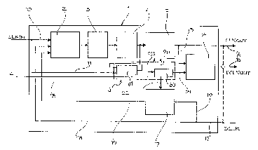
In the block diagram in Fig. 1, reference 1 indicates in its entirety a PLL circuit
which, according to a configuration known in itself, comprises the following elements
35 or modules:
- a phase/frequency comparator 2 having associated, as output circuit, a circuit 3 of
the type commonly called "current pump",
CA 022~3~83 l998-ll-04
. ,
- a loop filter 4 which receives the output signal of the current pump 3,
- an osci~lator 5, configured as VCO (voltage-controlled oscillator) and driven by the
output signal of the loop filter 4,
- a first frequency divider 6 which acts on the output signal of the oscillator 5,
5 - a second frequency divider 7 inserted, in the way that shall be better described
hereafter, in the feedback loop of the circuit, and
- a general control module 8 destined to allow the reconfiguration of the circuit in the
way better described hereafter.
In particular control module 8 has been shown here as being ideally subdivided
10 into two parts, indicated as 80 and 81 respectively. Hereafter, for the sake of
simplicity, the term "control module" will also be used to indicate each of the two parts.
Of such two parts, the part 80 performs the normal function of controlling the
operation of the PLL, in particular by intervening on the oscillator 5 as well as on
dividers 6 and 7 according to a configuration signal Cl coming from outside through a
15 line 13. The references 20, 21 and 22 show three lines through which the control
module 80 acts, respectively, on the oscillator 5, on the first divider 6 and on the
second divider 7. The part 81 instead is specifically dedicated to controlling the
operation of the oscillator 5, through a line 200.
The clock signal for which the phase lock and/or frequency lock and
20 multiplication functions are to be performed accorcli"g to the embodiment described
herein has been denoted CLKIN. This signal is carried through a line 10 to the input of
the comparator 2 and, through a line 11, to one of the inputs of the control module 81.
The latter also receives, through a second line 12, a driving signal related with the
output of the comparator 2, in particular the output signal of the loop filter 4. This
25 choice is anyway not to be taken as mandatory: an essentially similar function could
be performed, for instance, by the output of the current pump 3. In any case, driving
the control module 81 starting from the output of the loop filter 4 is found
advantageous because this allows taking advantage of the filtering action of the filter
4 itself.
The output signal CLKOUT of the oscillator 5 constitutes the output signal of
the circuit, present on a line 14. The same signal is also sent, through a line 15, to the
divider 6 which derives therefrom a frequency-divided output signal DCLKOUT,
present on a line 16.
A feedback signal FBLCK, present on a line 17, is fed back towards the
35 comparator 2 both through a direct line 18 and through a secondary line 19 which
passes through the second divider 7. As is easily understood by the person skilled in
the art, the accessibility of the line 17 from outside the circuit 1 is destined to allow a
CA 022~3~83 1998-11-04
greater flexibility in closing the feedback loop.
The feedback action towards comparator 2 can therefore be effected both
starting from the output signal CLKOUT present on the line 14 and starting from the
frequency-divided signal DCLKOUT present on the line 16, as well as from any other
element positioned downstream of the lines 14 and 16. This choice can be found
advantageous to take into account, for instance, additional phase displacements that
may be induced by those downstream elements. In any case this is a preferential and
not mandatory choice and, in the remainder of the present description, it may ideally
be imagined that the feedback line 17 is simply closed on the output line 14 as
10 schematically shown in Fig. 1 with a dashed line.
Similarly optional is the presence of two dividers 6, 7 whose function is to
generate a frequency divided output signal DCLKOUT and, respectively, to allow the
frequency multiplication.
The splitting of the feedback path into the two lines 18, 19 is destined to
15 account for the fact that, in essential analogy with what has been stated above in
regard to the output of the circuit 1, the divider 7 may introduce in the feedback loop
delays that cannot be exactly determined. Hence one can provide, according to
known criteria, for the circuit 1 to be activated initially by making the comparator 2
exploit, as feedback line, the "direct" line 18, thereby allowing the desired locking
20 conditions to be reached in the circuit. When this condition is attained, the comparator
2 can then take into account the signal present on the line 19 wherein the divider 7 is
inserted. This allows the latter to perform its function (in practice, in the form of a
"decimation" of order N of the pulses comprising its input signal) without modifying the
lock conditions set by using the direct line 18.
A preferred characteristic of the circuit 1 (characteristic which is not shown for
the sake of simplicity in the general diagram in Fig. 1, but which can be seen, for
instance, in Figs 2 and 4, relating to the individual elements) is the use of a differential
structure at least for the current pump 3, the loop filter 4 and the oscillator 5. The term
differential structure is meant to indicate in general a structure wherein the signal
30 transferred from one element to another actually comprises the difference between
the signal values (typically voltage values) present on two complementary lines,respectively positive and negative (or inverting). This choice offers, among other
factors, the advantage of offering a lesser sensitivity to noise, in particular to noise on
the power supply, also giving rise to a lesser generation of disturbances (for it is
35 possible to work with smaller and complementary signals, with circuits that operate in
linear zone).
The diagram in Fig. 2 shows in greater detail the structure of the oscillator 5,
CA 022~3~83 1998-11-04
constructed, as stated above, according to the typical configuration of a Voltage
Controlled Oscillator or VCO. The structure is known in itself, but it is shown to ease
understanding of the invention.
In the embodiment shown, the oscillator 5 comprises three delay elements or
5 stages 23 connected in cascade: The drawing clearly shows the complementary
structure of the respective connecting lines 24 as well as of the feedback line 25
which connects (in an inverting manner, i.e. by creating a negative feedback) the
output of the delay element 23 farthest downstream with the input of the elementlocated farthest upstream.
10The reference 26 indicates an output buffer circuit which acts on the output
signal of the element 23 farthest downstream thereby making it suitable for being sent
on the line 14 (and on the line 15, if present).
The reference 27 indicales a control circuit that receives at its input (preferably
in complementary configuration, through two lines indicated respectively as 40 and
1541) the output signal of the loop filter 4. The circuit 27 further requires, as
configuration control signals, the signals incoming on the lines 20 and 200.
The oscillator diagram shown in Fig. 2 provides for frequency control to be
effected by varying the output impedance of the individual stage (or element) 23, aiso
aiming at obtaining a constant voltage range at the output of the individual stage. The
20 related control procedures starting from module 27 essentially correspond to those
described for instance in the work "Fully Integrated CMOS Phase-Locked Loop with15 to 240 MHz Locking Range and + 50 ps jitter" by llya Novof et al., in ISSCC Dig.
Tech. Papers, February 1995, pages 112-113.
The control module 80 acts on the module 27 through the input 20 in the way
25 described in the aforementioned work by Novof et al., in particular with reference to
Fig. 7, thereby allowing constructing the filter 4 as an essentially capacitive
component, and also controlling the damping of the circuit according to the division
factors of the dividers 6 and 7.
The control module 81 acts on the module 27 through the input 200 in such a
30 way that the VCO operates according to one among several frequency/voltage
characteristics as shown schematically in the diagrams of Figs. 3A - 3C.
These Figures correspond to the behaviour of the frequency/voltage
characteristic of the oscillator 5 measured under three different conditions, and in
particular under three different temperature levels and three different results of the
35 technological process, namely:
- very high ambient temperature (for instance 80~C) and slow process parameters
(Fig. 3A),
CA 022~3~83 1998-11-04
- normal ambient conditions (25~C) and typical process parameters (Fig. 3B),
- rather cold ambient conditions, such as those which may occur as an effect of
exposing the circuit to the action of a refrigerating device, and fast process
parameters (Fig. 3C).
The terms "fast parameters" and "slow parameters" have been used since the
variability of the results of the technological process translates in practice into a higher
or lower operating speed of the conlponent.
For each condition, there is a family of characteristics (eight in the embodiment
shown). The various characteristics in each family correspond to a different
10 configuration whereby the oscillator 5 is driven by the circuit 27, i.e. to a number of
different behaviours of the output frequency versus the input voltage for different
values of the logic combination applied on the line 200.
By way of example it can be imagined that the lowermost characteristic in Figs.
3A - 3C corresponds to an input logic combination "000" on the line 200, whereas the
15 uppermost characteristic corresponds to a different combination, such as "111". Of
course, while retaining the principle unchanged, the described embodiment may beimplemented by using a greater or smaller number of characteristics or yet again, at
least theoretically, with the possibility of choosing the individual characteristic adopted
within a range that is no longer discrete (as in the case of the embodiment shown) but
20 continuous or essentially continuous.
It should further be observed that, whilst the present detailed description refers
specifically to temperature as the parameter determining the variation of the
characteristics, a behaviour of the same nature can be noted - mutatis mutandis - as a
function of other parameters such as power supply voltage or other variables of the
25 integration process.
The parameters represented by the characteristics highlighted above may be
critical for the correct operation of the device.
For example, it is possible to demonstrate that the pulsatance corresponding to
the cut-off frequency of the transfer function of the phase of the PLL can be
30 expressed with the following relation
~12Kd Ko (I)
where ci)n iS the pulsatance in question, N is the division factor of the divider 7 (if
present; should that divider not be present, then N=1), C is the capacitance value
corresponding to the behaviour of the filter 4 whilst Kd and Ko are the sensitivities of
35 the comparator 2 and of the oscillator 5.
Specifically, the (current) signal 4 generated by the set of comparator 2 and
CA 022~3~83 1998-11-04
current pump 3 can be expressed as
id = Kd~3e (Il)
where ~e iS the phase deviation present at the input of the comparator 2.
The pulsatance ~O at the output of the oscillator 5 can instead be expressed by
the relation
oo = K~Vc (111)
where Vc represents the signal (in voltage, usually differential) at the input of the
oscillator.
Formula (I) allows understanding that the impossibility of synthesising high
10 values of capacitance C compels to keep low the value of the product Kd Ko in order
to keep the value of the pulsatance ~n limited. In practice, for the frequency values
indicated in the introductory part of the specification, it is preferred for that pulsatance
to remain at values corresponding to frequencies in the order of 1 - 2 MHz. Value Kd,
indicative of the sensitivity of the comparator 2, cannot decrease below a certain
15 value because of the need to prevent the signal itself from being excessivelypenalised by noise. Hence the need arises to try to limit as far as possible the value
Ko, representative of the frequency/voltage gain of the oscillator; this also prevents
the oscillator itself from excessively amplifying the noise present at the output of the
filter 4.
Thus, for instance, a PLL essentially similar to circuit 1 described here, wherein
however the VCO 5 presents a single operating characteristic, for instance the
uppermost characteristic in the three diagrams in Figs. 3A - 3C, could be overall
acceptable in the case of operation at 80~C (Fig. 3A). However, it would be wholly
unacceptable (because it would correspond to an excessively high value of gain) in
the case of operation at 0~C (observe the uppermost curve in the diagram in Fig. 3C).
The provision, according to the invention, of an oscillator 5 with variable
characteristic, in particular with the possibility of being made to operate according to a
frequency/voltage characteristic selectively identified within a range of available
characteristics, allows optimising the operation of the circuit by adapting the behaviour
of the oscillator 5 to the specific conditions (temperature, power supply voltage,
process parameters).
For instance, it is possible, when operating at a temperature in the order of
25~C and under typical process conditions, to make the control module 81 intervene
on the oscillator 5 to make it operate with the characteristic corresponding to the third
curve from the bottom in the diagram in Fig. 3B. When the circuit 1 operates, for
instance, at about 80~C, the same module 81 can intervene on the oscillator 5 in such
a way as to make it operate according to a characteristic corresponding to the sixth
CA 022~3~83 1998-11-04
curve starting from the bottom in the diagram in Fig. 3A. Lastly, when operating, for
instance, at about 0~C, the same module 81 can intervene on the oscillator 5 in such
a way as to make it operate according to the characteristic 1, i.e. the lowest one in the
diagram in Fig. 3C.
By comparing the various diagrams in Figs. 3A - 3C one can see that the
practical effect of the adaptation function just described is that of keeping limited and
essentially constant the sensitivity of the oscillator 5 as the parameters vary.The adaptdLion of the operation of the oscillator 5 can be effected, as a
function of the working frequency, as a veritable calibration action effected on the
10 circuit. Once the circuit manufactured, (for instance in the form of an integrated
circuit), its operation can be adjusted according to the conditions of use in such a way
as to optimise its behaviour, for instance, as a function of the process parameters
(generally not controllable a prion).
Figs. 4 and 7 refer to a preferred embodiment where such adjustment
lS becomes an automatic adaptation function. The circuit can thus be configured in such
a way that, upon activation, it is able to place itself automatically on the operating
characteristic of the oscillator 5 that corresponds to the desired optimal conditions,
with the possibility of subsequently choosing another characteristic when the one
adopted previously is no longer to be considered optimal.
In this regard one should however take into account that, especially in
applications to the synchronisation of complex circuits, the transition of the oscillator 5
from one operating characteristic to another may constitute an undesired
phenomenon, as it may give rise, for instance, to a "jump" of one period in the clock
signal. In those applications it seems therefore preferable, once a given characteristic
25 is adopted upon circuit activation, for the oscillator 5 to be maintained on that
operating characteristic even when it has become sub-optimal, except in presence of
sizeable phenomena (for instance a strong variation in the input frequency of the
device), such as to make the adopted characteristic so unsatisfactory that the onset of
a negative phenomenon like the jump of one synchronisation period is nevertheless
30 preferable to continuing operation on a characteristic that has become sub-optimal.
The diagrams in Figs. 4 and 6 show, together with Fig. 8, the possible
embodiment of such a function of automatic tracking of the optimal characteristic
followed by a function of permanence on such characteristics so as to prevent, or in
any case to make very improbable (except in case of a radical change in the operating
35 conditions of the device), further characteristic changes. As shown previously in Fig.
1, the aforesaid function is driven by the output signal of the loop filter 4 (line 12 of
Fig. 1, shown in the diagram in Fig. 4 in its differential configuration).
CA 022~3~83 l998-ll-04
In Figure 4, the reference 30 indicates a configuration control circuit whose
output essentially corresponds to the line 200. In other words, the circuit 30 allows
making the VCO 5 operate according to a characteristic selectively determined.
The circuit 30 operates when enabled by the input clock CLKIN present on the
5line 11 and under the control of two signals, respectively defined as rising (UP) signal
and falling (DOWN) signal: the sense of "up" and "down" is taken here as the onecorresponding to the order according to which the characteristics are presented in the
various diagrams in the Figures 3A- 3C. In practice, the UP signal determines such
an intervention of the configuration control circuit 30 as to lead the oscillator 5 to
l0operate on a higher characteristic than the one where it is currently located. The
DOWN signal determines an intervention in the opposite direction.
The DOWN and UP signals are produced by a comparator circuit 31
essentially consisting in a double comparator with hysteresis having the
characteristics shown in Figs. 5A and 5B. In these Figures the values of the
15differential input signal Vc present on the lines 12 are plotted in the x-axes. The y-
axes correspond instead to the UP signal (in Fig. 5A) and to the DOWN signal (in Fig.
5B). For the sake of clarity, the "high" value corresponds, in both Figures, to the active
state of the related signal, with consequent change in the operating characteristic of
the oscillator 5. The "low" value corresponds instead to the absence of output signal.
20In practice, when both output signals are at the "low" value, the operating
characteristic of the oscillator 5 is retained unaltered.
Once the desired operating characteristics are known, the realisation of a
circuit of this kind constitutes, for the person skilled in the art, a normal design task.
For this reason, in order not to overburden the presentation of the invention, a25detailed description of the structure of the circuit 31 is not provided herein.
As better shown in Fig. 6, the circuit 30 essentially consists in a state machine
301 which reads the UP and DOWN signals at the instants identified by a clock signa!
generated internally, by means of a divider 302, starting from the signal CLKIN
present on the line 11, and in a decoder 303 that converts the states of the machine
30301 into logic signals suitable for driving the block 27. The state diagram of state
machine 301 and the related transitions are shown in Fig. 7.
Fig. 8 refers, for the sake of simplicity and clarity of illustration, to the family of
operating characteristics shown in Fig. 3B and shows the two pairs of threshold
values V1, V2 and -V1', -V2' of the comparator 31.
35Still with reference to Fig. 8, let it now be supposed that, upon its activation,
the circuit 1 is operating in the point indicated as to ("entry" state). In this state, the
oscillator 5 operates at minimum frequency, regardless of the control voltage Vc. This
CA 022~3~83 1998-11-04
11
frequency is far lower than the desired one, chosen herein by way of example to
correspond to 622 MHz and represented in the figure by a horizontal dashed line.Jhe general feedback function of the circuit leads then to a voltage increase atthe input of the oscillator 5. However, such an input voltage increase is not
S immediately translated into an increase in the operating frequency of the oscillator 5
which continues operating at the frequency corresponding to point to until the input
voltage of the oscillator 5 reaches the threshold V2 of the circuit 31.
Once this threshold is reached, the circuit 31 emits the UP signal and, in
co~ por)dence with the suhsequent rising front of CLKIN, the state machine passes to
10 state 1, thereby selecting the first ch~,~~ri~Lic. Under those conditions, the operating
frequency of the oscillator 5 increases rapidly as is illustrated schematically by the arrow t1
Upon reaching the cross-over point between the voltage value V2 and the first
characteristic, the operating frequency of the oscillator is still lower than the desired
value of 622 MHz and consequently the UP signal is still active. As a result thereof,
although it has performed its function of tracking the desired frequency on the first
characteristic, the comparator 31 intervenes (UP signal) on the configuration control
element 30 thereby causing the osci"~tor to operate on the second characteristic, as
shown in t2 at the right-hand side of Fig. 8 (passage to state 2).
All this translates, depending on the voltage value present at that moment at
the input of the oscillator, into the recognition of the fact that the frequency generated
by the VCO 5 exceeds the desired one. The oscillator 5 thus starts to track the
aforesaid frequency by descending backwards along the second characteristic,
thereby returning at this point within the upper band V1, V2 of the comparator with
hysteresis 31 and becoming stabilised at the working frequency. Although the circuit
operates correctly, the working point is not satisfactory because it is at the limits of the
characteristic and there is little margin to track variations in the operating conditions.
As a result, the comparator continues to present an UP command, which in t3 causes
circuit 30 to change state, thus leading the oscillator 5 to operate on the third
characteristic (state 3).
At this point, performing the backward tracking function on the third
characteristic, the oscillator 5 moves to the desired operating point (arrow t4), which
as shown corresponds to an input voltage lower than V1 and to an output frequency
equal to the desired frequency of 622 MHz. Now the UP signal is at a low level and
the circuit becomes stabilised in the aforesaid operating condition, remaining there
even in the presence of rather marked changes in the behaviour of the VCO 5, duefor instance to temperature variations, provided - however - that such changes do not
cause the oscillator 5 to depart from the central band comprised between the extreme
CA 022~3~83 1998-11-04
12
switching levels (V2, - V2') of the comparator with hysteresis 31.
In the presence of a very marked change in the operating conditions, for
instance in the input frequency, the control voltage exceeds V2 or drops below V2'
and a new characteristic is chosen as described above. The result is the generation,
S by the circuit 31, of the UP or DOWN signal so as to cause, through the configuration
control module 30, the oscillator 5, to move to the desired characteristic.
Of course, while the principle of the invention remains unchanged, the
construction details and the embodiments may be widely varied with respect to what is
described and illustrated herein, without thereby departing from the scope of the
10 present invention. For example, one could think of directly controlling the stages 23 of
the oscillator 5 with the signal 200.