Note : Les descriptions sont présentées dans la langue officielle dans laquelle elles ont été soumises.
CA 02254132 1998-11-05
WO 97/44805 PCT/US97/08727
MULTI-STAGE ELECI'RON GUN HAV~NG AN ELECrROSTAllC CAVITY
FIE~ D OF THE INVENTION
The present inveMion is related to electron ~uns. More specincailv, the present invention
is related to an electron gun that uses an elec-rostatic field to radially focus and a~iallv accelerate
a DC e'ectron bearn.
BACKGF~OUND OF THE INVENTION
The development of reliable~ non-cont~min~ting and long-life (robust) hign-c~nrre:lt
e!ec~ron beam sources for injec.ion into ki~strons and related devices has bee:l a challenginE
problem for many years. High-c.nrrent beams are widelv used in injee:or syste.ns for electron
accelerators, both for industrial linear accelerators (linacs) and hi_n-enern accelerators.
High-current electron be~ns are also used for microwave generatioA (in ~l~strons and related
devices), for research on advanced methods or particle acceleratio~ and for inje~ors used for
free-electron laser (FEI,) drivers. Durin~ the last fe v years considerabie e~rort has been applied
to the development of high power linac injectors [J. L. ~mc~; et al., IEEE Trans. ~-ucl. Sci.
~iS-32. 3397 (1985); T.F. Godlove, et al, Part. Accel. 3~, 169 (l9ao)] and particularly to
laser-inili~ted photocathode injectors [J. S. Fraser and R. L. Sheffie!d. IEEE J. Quantum Elec.
QE-23, 1489 (1987); P. Schoessow. E. Chojnaclci, W. Gai, C. Ho, R. Konecny, S. Mtingwa, J.
~'orem, M. Rosing, and J. Simpson, Proc. of the 2nd Euro. Part. Accel. Conf. p 606 (1990)~
rhe best of the laser injectors have relatively high bearn quality, but their reliabiii~ depends on
the choice of photocathode material, with the more reliable materials requirine intense laser
illllmin~tion.
The high-density electron gun invention to be described here is called a Robust Pierce
Gun (RPG). [See "Theory and Design of Electron Beams", J. R Pierce, D. ~an Nostrand
Company, Inc. (1954)]. The RPG avoids the difficulties associated with plasma cathodes,
CA 022~4132 1998-11-0~
WO 97/44805 PCT/US97/08727
thermionic emitters. and ie d emission c~thodes. Plasma ealhodes canncl be ~oe ated ~t hi_
repetition rate, nor can ;hey suslain ve.~v long pulses without volta~e c~llapse. The rn onic
emitters are only good for low c.lrrent densities (~0 .~rnps~c n-), and are easii~ com~rnin~ted.
Field emission cathodes require a huge field (- 109 ~Vim) for reasonable emission.
Laser-initiated photocathodes require an e~cpensive laser system and suffer from reliabilitv issues
in high e!ectric fields.
High current-density beam generation me~hods used to date are rather comple~
cumbersome, e~cpensive, and have very definite limits on pe.torrnance. The RPG described he e
is promisin_ in large part because of the natural current amplificafion process inne ent in
secondary electron emission. This natural amplincation process m2~;es possible asimply-designed gun wnich could provide a cold c~thode al high-current dens.ties operating a.
modest duty factors and rela~ive!y high-qualiry pulsed electron beams suilabie for mam
applications.
SUMnAARY OF THE INVENTION
The present invenfion reiies upon amplifying, by means of secondary electron ernission, a
beam of electrons produced by a reliable low-current-densitl, electron emitter. The invention is
based on the ph~omP~nn of l,~ "~ ed secondary electron production from surfaces or
ne~ative-electron-affinit,v (~EA) materials [R. U. Martinelli and D. G. Fisher, Proc. of the EEE
62, 1339 (1974); H. Bruining, Physics and Applications of Secondary E ectron Emission
(Pergamon Press, London, 1954), incorporated bv reference herein]. ~ beam of electrons
(primary beam) is accelerated in a cathode/anode configuration to impinge on a film elec~rode
(which has a thiclcness to allow the tr~nsmiccion mode of operation) of an ~EA material.
Depending on the range of the electrons in the film e!ectrode, secondary e'~ectrons are then
created prefelellLially on the bac~side of the thin film electrode, that is. in the direcro~r of
propaganon of the primary beam. Current amplification through one stage or a ~A material
like di~ml~n~l could be over 50 times. To accomplish amplification of the electron current
CA 02254132 1998-11-05
WO 97/44805 PCT/US97/08727
density. one or more stages of secondar emilter films are utiiized alon~ ~~ith one pr;.mary
emitter. The pr mary ernitter is a low-current-density robust emitter (e.g, thoriated tungslen).
E~camples of NE.~ materials are GaAs, GaP, Si, diamond, and malerials used as photoernitters,
secondary electron emitters, and cold-cathode ernitters.
The first col,lpone~-L of the present invention pertains to the elec ron gun. The electron
gun comprises an electrostatic cavity havine a first stage with emitting faces and multiple staees
with emitting sec ions. The gun is also comprised of a mPch~nicm for producin_ an electrostatic
force which encompasses the ernitting faces and the multiple emitting sections so elec~.rons are
direc.ed from the ~m;tting faces toward the ernitting sections to contact the emitting sec ions and
generate additional electrons and to further contact other ~nnittin~ sections to generate additional
electrons and so on~ then finally to escape the end of the cavity.
The e.mitting sections preferably provide the cavity with an acce!e ating ~or.e for
electrons inside the cavity. The multiple sections preferablv include for-~,ard ernitting suraces.
The forward emitting surfaces can be o~ an annular shape, or of a circular snape. or of a
rhombohedron shape.
The mech~ni~m preferably intl~ldes a mech~nicm for producing an electrostatic electric
field that provides the force and which has a radial component that prevents the e!ectrons from
straying out of the reg~on between the first stage with ~mitting faces and the multipie ~~mirting
sections. Additionally, the gun in~lltdes a mech~nism for producin_ a magnefic field to contain
the electrons anywhere from the first sta~e with emitting faces or any emittin_ section and to the
end of the ca~ity.
The first component of the present invention pertains to a method for producing a flow of
electrons. The method coll,p,;ses the steps of moving at least a first electron in a first direction at
one location. Ne~t there is the step of striking a first area with the first electron. Then there is the
step of producing additional electrons at the first area due to the first electron. Ne~t there is the
step of moving electrons from the first area to a second area and ~r~ g electrons through
CA 02254132 1998-11-05
WO 9714480S PCTIUS97/08727
the second area and crea~ing more electrons due to electrons from the firsl ~rea striic;ng the
second area. These newly created electrons from the second area move in the firs; direc.ion then
strike the third area, fourth area, etc. Each area creates eYen more elec;rons in a repeatin_
manner by the e'ectrons moving in the first direction to multiple are~s. This process is also
repealed al di~e~e,.~ Iocations.
The mer~nism preferably inrludes a me~h~nism for accelerating the ele~.rons inside the
cavity to allow the electron multiplication to continue.
The electron preferably includes a comrol grid for interruptinr the flo-~ of elec:rons and
thus to create bunching ofthe e!ectrons.
The present inveMiOn pertains to an electron gun. The electron g~n comprises an
electrostatic cavitv having a first stage with eleclron ~mitting faces and mui~ipie slages with
electron emittin~ sections. The electron ~un also comprises a mechanism for producing an
electrostatic force which encompasses the e!ectron emittin~ faces and the multiple e!ectron
emitting sections so electrons from the e!ectron ~mirting faces and sections are cireF.ed from the
emitting faces toward the ~mitting sections to contact the Pmjtting sec;ions and generate
additlonal electrons on the opposite sides of the ernitting sections and to further contact other
emlthn~ secnons.
The present invention pertains to a method for producing electrons. The method
comprises the steps of moving at least a first electron in a first direction from a first location.
Then, there is the step of striking a first are~ with the first electron. Next, there is the slep of
producing additional electrons at the first area due to the first electrons on the opposite side of
the first area which was struck by the first electron. Next, there is the step of moving e}ectrons
from the first area to a second area. Then, there is the step of ~ c~ )g electrons to the
second area and creating more electrons due to electrons from the first area s~riking the second
area.
CA 02254132 1998-11-05
WO 97/4480~; PCT/US97/08727
BRIEF DESCRIPTION OF THE DRAWINGS
In the acco,.,l~r,~ing drawings, the preferred embodimen~ of the invemion and plt:.re.,ed
methods of practicing the invention are illustrated in which:
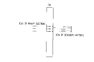
Figure 1. Sch~m~tic drawing of the current m-lltiplir~inn process. .~ low-curreM electron
beam from a robust primary cathode is made to enter a material with a negalive-elec~.ron-a~nity
(NE.~) surface. The layer thickness is chosen so that the range OI the primarv electrons is less
than the film thickness. The bulk of the primary beam ener~ is de?osited in the negative
e!ectron affinity (NEA) material where the secondary e!ectrons e~l in the dow-nstream direction.
Figure 2. Schematic drawing of a two-stage robust Pierce gun (RPG). ~ lo~-current e!ectron
be~m from a rugged and long-life cathode (- 0.0145 Amp/cm') impin~es on a ne_afive e!ectron
affinity (NEA) surface. A high-current density beam is achieved bv meqns of secondary electron
emission (typically producing several te~s of secondaries for eac:l primarv). There is a second
arnplification stage to further increase the current density to say 30 ~ mps,'c;r.~.
Figure 3. Illustration of tr~ncmission and reflection modes or secondarv electron emission.
Secondary ernission gain curve for a 2.~ rnicron thiclc Si dynode [R U. ~IarTinelli and D. G.
Fisher, Proc. of the lkkE 62, 1339 (1974)]. Shown are data for re~ected (top curve) and
tr~ncmitted (bottom culve) secondary electrons. The described invention utilizes secondary
electron emission in the tr~ncmic~cion mode.
Table L Summary of some known NE.~ materials with the corresponding adsorbates. In
practice, the adsorbates are not denoted in the literature when referring to a parlicular material.
Figure 4. Secondary electron coef~icient vs. primary electron energy for CVD diamond in the
reflection mode. The data represented by the filled-in spades (upper curve) represent CVD
~i~mnn~ a~er depos;~ion of a 10 nm thick CsI surface layer. The open triangles (lower curve)
CA 02254132 1998-11-05
WO 97/44805 PCT/US97108727
re?resent that obtained from CVD diamond wlithout an applied surface layer [G. T \~e rini, I. L.
Krainsl~y, J. A. Davton, Jr., Y. Wang, C. .~. Zorman, J. C. ~ngus, R. W. Hoffiman, D. F.
Anderson, Appl. Phys. Lett. 66, 242 (Ig95)~.
Figure 5. Electron charge density profile as a function of posifion in diamond film. This result
is for S keV electrons normally incident on a 1 ,um thiclc ~i~mond fiim. 5 keV primary electrons
are optirnum for the production of seCon~l~ry electrons.
T~ble IL Ernission characteristics of se!ected cathode materials as a fimction of temperature.
Figure 6. The steady-state temperature distribution for the case of two stages of secondary
emission after the primarv cathode. This is the temperature distriDulion in the first and second
diarnond emitter films due to e!ectron beam bombardment and radiam heatin_ from the primarv
cathode and secondary emitter films. The fiim is a~s-~med to be al room temperature at its
peripheral boundary.
Figure 7. SchPm~tic cross-section drawing of a robust Pierce gun (RPG). In this case. the
primary cathode is of a thermionic type and is made of thoriated mnosten Shown are two stages
of secondary electron ~mplifir~tion. The dimensions are accurate for building an RPG.
Figure 8. Schematic replr~ t~ on ofthe robust pierce gun.
DES~RIPTION OF THE PREFERRED EMBODIMENT
Referring now to the drawings wherein like reference numerals refer to similar or
identical parts throughout the several views, and more specifically to figure 8 thereof, there is
shown an electron gun 10. The electron gun 10 comprises an electrostatic cav~ty 12 having a
first stage 14 with electron P~ faces 16 and multiple stages 18 with electron emi~ing
sections 18. The electron gun 10 also comprises a mech~nicm 15 for producin_ an electrostatic
CA 02254132 1998-11-05
WO 97/44805 PCT/US97/08727
force which encompasses the e!ectron emitting faces 16 and the multiple elec~ron emitting
sections 18 so elec~.rons from ~he electron l mi~ting faces 16 and sec~ions 18 are direc-ed from the
emitting faces 16 toward the emi~ing sections 1~ to contact the emir~inY sections 1~ and
generate ~ditiorl~l e!ectrons on the opposite sides OI the ernitting sections 18 and tO further
contact other çmirtinY sections 18.
The emitting sectionc 1~ preferably provide the cavity 12 with an accelerating force for
electrons inside the cavity 1~. The multiple sections 18 preferably inc!ude forward e.nitting
surfaces. Preferablv, the forward emittino surfaces are of an annular shape. .~lternativelv, the
forward emitting services can be of a circular or a rhombohedron shape. Preferabi~, the
~mi1tinsJ sections 18 provide the cavitv 12 with a force to acce!erate electrons to a higher energv.
The mech~nism 15 for producing an e!ectrostatic force prer~rably inc'udes a me~h.~ni~m
17 for producing an electrostatic electric field that provides the force and which has a radial
component that prevents the electrons from straying out of the re~on between the first stage 14
with çnnittinF faces 16 and the multiple emitting sections 1~. The e!ectrostatic force producin_
merh~nicm 15 preferably inr!ud~s a merh~ni5m 19 for producing a flow of electrons from a first
stage 14 with k,.,;~ Q faces 16 or any emitting section 1~ and to the end of the cavirv 12. The
producing mPrh~nicm 15 preferably in~lnde5 a me~h~ni~m 2J for producing a magnetic field to
confine the electrons to contain the electrons anywhere from the first stage 14 wilh ernit~ing
faces 16 or any ~ g section and the end of the cavity 12. Preferably, the ~un 10 inclllde5 a
grid 25 for bunching electrons. The gun 10 can be used, for instance, for RF sources of energy
and for injectors.
The present invention pertains to a method for producing electrons. The method
comprises the steps of moving at least a first electron in a first direction from a first location 21.
~ Then, there is the step of striking a first area 20 with the first electron. Ne~t, there is the step of
producing ad~ition~l electrons at the first area 20 due to the first electrons on the opposite side of
the first area 20 which was struclc by the first electron. Next, there is the step of moving
electrons from the first area 20 to a second area 22. Then, there is the step of tr~n~ g
.... . .
CA 02254132 1998-11-05
WO 97/44805 PCT/US97/08727
elec.rons to the second area ~ and c.eafin~ more elec~.rons due to e!ec-rons from the first area ~0
striking the second are~".
The RPG inveMion emplovs the emission of secondary elec2rons in a tr~n~mi~ion mode
as opposed to the conve~tional mode of reflec ion, i.e., electrons e~cit from the bac~; face of a
negative electron affinity (NEA) materialt and in the sarne direction as the incident be rn Figure
1 shows the basic idea of a primary electron beam being deposiled into a foil or film of a
secondary emitter and the emergence of a seCon~ry bearn in the same direction as the primary
beam. Figure 2 shows the overall idea where electron current amplification is accomplished in
two stages of secondary ernitters. The primary emitter is a low curreM densitv robust emitter
(e.g, thoriated tllng~ten). The secondary ernitters are ~EA electrodes which emil secondary
electrons in the same direc ion as the inc dent beam. Specir~c app}ication is targe~ed for
klystron guns in the curreM densitv range of up lo seve. al tens of amps/cm-, pulse lenvr.hs in the
multi- nicroseconds, and repetition rates up to several hundred pulseslsecond.
Figure 3 illustrates the tr~n~mic~ion and reflection secondary emission properlies of an
~A material, in particular cesiated silicon. The secondary electron ernission yield in the
tr~n~mi~sion mode for this parlicular NEA material is very large. For e~cample, the secondary
emission coef~icieM for the tr~nsmitted eleclron current (i.e., the secondaries which leave the
bac~ surface of the material and travel awav from the cathode) is 100 (for primarv electron
energies of 10 keV) to 1000 (for enervies of ~0 keV). The yield for the reflected electron current
(i.e., the usual case in which secondaries are ernitted off the,t~ont surface of the material and
travel baclc towards the primary cathode) is 1000 for energies iO-~O keV. However, because
cesiated silicon is sensitive to co~ "il~tion, a better material is cesiated diamond as the
secondary ernitter. The NEA electrode materials of choice are chemical vapor deposited (CVD)
diamond films. This new terhnology has shown great promise in developing high yield robust
secondary emission materials.
A negative electron affinity surface is a material for which the difference betvveen the
bulk conduction band miniml~m and the Fermi level is greater than the work function. If this
CA 02254132 1998-11-05
WO 97/44805 PCT/US97/08727
condition holds, an electron ~vi~h enerFY greater than or equal to the conduc:ion band minimnn
energy encounters no worK func~ion barner at the serniconduc or surface. To acnieve this
condition, the worlc function of a semi-conductor is reduced by the adsorption of elec~roposi~ive
elements (and som~t-m~s bv a combinalion of elec~ropositive and ele~rone2ative e!ements) tO
atomically clean surfaces of the material. Cesium (Cs) and Oxygen (O) are the most popular
adsorbales used. Comrnon ~A mare:ials are made from GaAs (Cs and Cs-O used as
adsorbates), Si (Cs-O and Rb-O used as adsorbates), and s~milar tvpes of materials. A summarv
of some knourn NEA surfaces wi~h the corresponding adsorbates is given in Table I.
Materis~ dsorbate
GaAs Cs. Cs-O. Cs-F
GaP Cs
(IIL Ga)As Cs-O
InP Cs-O
GaSb Cs-O
Si Cs-O. Rb-O
AlAs Cs-O
Diamond CsI (KCI. NaCI)
Table L
Most of these marerials are not robust, or not u~r ~riate for use as an amplificarion
stage. Chemical vapor deposited (cr~J films of diamond exhibit a stable ,~E~ condition wirh
high secondary electron emission (yields up tO ~ 50 at ~7 energy of 3 ke r7. These results were
done for primary dc current densities up to 50 mAlcm-, and the targets were coated with CsI
from 10 to 100 nm thick. The emission was activated by electron beam-induced iodine depletion
after short beam exposures. The resultin~ diamond surface is Cs termin~te~l and independent of
the initial CsI thickness; it e~hibits stability in air and baclc to vacuum again [G. T. Mearini, I. L.
CA 02254132 1998-11-05
WO 97/44805 PCT/US97108727
Krains~, J. A. Davton, Jr., Y. WanP, C. .~. Zorman, J. C. .~ngus R. ~V. Hoffinan. D. F.
Anderson, Appl. Phys. Lett. 66, 242 (1995), incorpora~ed by reference herein].
Figure 4 shows the secondary electron yield vs. primary energy for CVD diamond in the
reflection mode. The lower curve (described by the open triangles) is for uncoated diamond.
The upper curve is for C~TD diamond with a 10 nm thick CsI surface layer which converts the
surface into an NEA emitter.
The range of the primar,v electrons in the NE.~ material must be siighllv less than the
material thickness. Otherwise, the bulk of the beam energy will be deposited ne~r the front
surface of the eleclrode. Secondary e!ectrons will then be prefere,lliailv produced at this for vard
surface with a velocity back towards the cathode (i.e., con~entional secondar~ e!ectron
emission). If the range of the primary elec-rons is too large, the primarv electrons could tra~e-se
the layer completely. Either case will reduce the secondary emission yield of the device. In
addition. the primaIv electrons that make it through the NEA surface will ha~e a hi8her avera(Je
trans~erse velocity than the secondaries (which are emitted primariiv in the forihard direction).
The optimum ran8e for the primaries is a distance a little iess than a secondarv e!ectron di~ilsion
length.
Optimally, the thickness of the NEA amplification material should be equal to an e!ectron
diffusion length. The diffusion length of an NEA emitter is equal to the escape deplh, and is
determined by the peak in the secondary electron emission yield curve. For electron energies
larger than the peak some seCon~ries born dee? into the material will not ha~e enough energy
to escape. For electron energies smaller than the peak the m~imllm amouM of se~ondaries will
not be produced. It is only at the peak in the yield that the range of the primarv e!ectrons is equal
to an electron diffusion length in the material. The thiclcness of the NEA material should be a
little larger than an electron diffusion length.
CA 02254132 1998-11-05
WO 97/44805 PCT/US97/08727
11
~n electron diffusion length L is well known to be taken to be
L = (~kT~.le)m
where T is the temperature, k is the Blllt7m~nn constant, ~L is the ele~ron mobility, e is the
elec~tron charge, and ~ is the eleclron life~ime In eeneral, the diffusion len~ L is dependent on
the doping corln~ntration, the erowth melhod, and other factors. Opsimai NEA material
thit-l~n~o~c~s are 3-10 llm for Si, 3 to 5 ~m for GaAs, and 0.2 llm for GaP.
The diffusion length L is essenti~llv the distance over which a seconcar electron born in
the bulk of the material can travel before recombining across the band g ? In contrast, the
escape depth is the depth in the matenzl from which a secondarv elec:ron .an diffilse to the
surface of the maserial and escape. ~hen a secondary e!ectron is born in the ~ui~ of the material
and begins to migrate toward the materiai surface, it loses energy to the lattice ;hrou~h coilisions
at a rate of about 50 meV per collision with mean free paths between cnilisions of 25 to 50
anestroms. Typically, a seCon~ry electron produced in the material trave!s oniv a few hundred
an_stroms before its energy decays to the bottom of the conduction band, al which point it is in
thermal equilibrium with the lattice. Such a so-called therrnalized minoritv e'e~ron can survive
for a relatively long time before recombinin~. However, if there is a polemial barrier at the
material surface then such an electron does not have sufficient energv to esca?e into the vacuum.
In a conventional esnitter or a non-NEA ernitter just such a potential barrier e.Yisss so that unless
the secondary electron is bom within a few hundred angstroms of the surace, it will not have
sufficient energy to escape. This is why the escape depth in a conventional emitter is only of the
order of a few hundred al~LIulllS, a ~list~nce from one order to several orders of ma~nitude
smaller than the diff~ on length of the secondary electrons in the material. rne ~reat advantage
of NEA emitters is that this potential barrier is removed by treating the mase ial surface so that
the escape depth for seCon~y electrons in an NEA material is equal to the diltusion lenPsh, a
distance ûfthe order of microns.
CA 022 4132 1998 - 1 1 - 0 .
WO 97144805 PCTIUS97/08727
The lower curve in Fig. ~ shows the secondary elec,ron e.~.~ssion cur~,e n Ihe re~leclion
mode for uncoated diarnond fiim which is a conventional ernilte .~iln an escape de?th OI ~ few
hundred angstroms. At lower energies the secondary yield rises because the number of generated
secondary electrons increases with increasing primary energy and because at lower energies all
of the plhn~y electrons are stopped within a few hundred angstroms of the surrace so that all of
the secondary electrons produced c~n reach the surface with su~icient energy, to escape. For
incident energies greater than 1 keV the primary electrons pene~rate the malerial to a depth
greater than a few hundred angstroms so that not all of the secondary electrons produced can
now escape and the secon~r~ yield curve reaches a maximum and begins to fall off wilh
incident energy. In coMrast, the upper curve in Fig. 4 for the CsI-coated diamond. which is a
NEA ernitter, continues to rise with incident enerny suggesting an escape de?th comparable to
the diffusion length for electrons in the material. The diffi~sion ien~h can be ~ctim~ted from the
secondary yield for CsI-coated diarnond in Fig. ~ By using t..e universai ~ie!d curve [B.K.
Agarwal, Proc. Roy. Soc. 71, 851 (195~)].
;~ = .na:: ( 2 E /E max )
[iT (~/~ ) 1.3_(2_ii)]
the m~imllm of the secon~ty yield curYe is a~p~ ately ~ = 5~ at a maximum primary
energy of em," = S keV. Hence, the diffilsion length is just the range in this material for 5 keV
electrons which is calculated as follows.
Figure 5 shows the charge deposition profile for 5 keV electrons norrnally incident from
the left side on a one-rnicron thiclc layer of diamond film. It is e~ident that at these very low
electron energies PccPnti~lly all of the primary electrons are sto~ped within 0.3 micron of the
incident surface. Because S keV corresponds to the peak in the secondary ernission curve in Fig.
4, then from Fig. 5 the diffusion length is approximately 0.3 ~u. Hence, the thickness of the
NEA material should be a little larger than 0.3 ~Lm.
CA 02254l32 l998-ll-05
WO 97/44805 PCT/US97/08727
The ideal primary cathode should be chemically inert, and the rate of e~aporation of the
active material should be low. We have decided to employ thoriated tl~ngcten for the primalv
cathode because of its robust properties. Its advantage over pure tl~nPct~n is the fact that it emits
at lower temperatures (Table II). Operation at lower temperatures is important in issues such as
reliability and long life. Thoriated tllng~ten is also much more robust and less susceptible to
poisoning than coln~ g cathodes such as LaB6.
Thoriated
T Tungsten Molybdenum Tantalum
Tun~sten
(-K) (ampslcm-) (amps/cm-) (amps/cm-) v
(amps/cm-)
16009.27 x 10-' 2.39 x 10~ 9.1 ~ 10~ 4.06 ~ 10
18004.47 x 10 5 1.05 X 10~ 3.32 x 10 ' 0.43
2000 1.00 x10³ 2.15 x 10³ 6.21 x 10³ 2.86
2400 0.12 0.22 0.51
2600 0.72 1.29 2.~5
2800 3.54 6.04 12.53
Table II
Energr deposition by the primary electron beam causes heating of the thin diamond films
used as amplification stages. Also, radiation from the primary cathode of thoriated tun_sten
radiatively heats the amplification stages. The maximum yield of seconda~ emission for
ce~i~ted diarnond is 5~ at 5 keV. For two stages of amplification for the RPG, a primary beam
from the thoriated~ ngctPn cathode at 0.0145 A/cm2 will produce a secondary beam of 0.8
, . ~
CA 02254132 1998-11-05
WO 97/44805 PCT/US97/08727
14
Alcm' at the first NEA electrode, which in turn will generate 41 ~cm at the second
electrode. The NEA ~ mon~ films are used in the trancmission mode.
The peak power density on target is given by
P= jp(A/c.l~,-) xEp (eV) W/cm2
where jp and ~ are the current density and energy of the plimary electron beam respectivelv.
For 5 keV primary electrons, the peak power density on target in the first diamond film is N73
W/cm2 (for a 0.0145 A/cm beam) and for the second stage is 4 kUT/crn (for a 0.8 A/crn beam).
The total beam energy deposited by a 2 lls pulse in the first and second stages are 0.145 mJ/cm'
and 8 mJ/cm2, respectively. Since diamond film is used as a secondar~y emitter in the
tr~ncmission mode, its thi~nl~ss is determined by the range of the 5 keV prima~ electrons. It is
0.3 mm, a thickness that poses no problem for the diamond film fabricators. The temperature
rise in the film due to a single pulse can be calculated from
mcp~lT=Q
where m is the mass, cp = 0.42 J/~-~C is the specific heat capacity of diamond, ~T is the
temperature rise and Q is the enerEy deposited. For the thickness used in this case, the deposited
energy by one single pulse will raise the te.l,~eldture of the diamond film by 3.6 ~C in the first
stage and l 8 l ~C in the second stage.
During operation, the di~montl secondary cathode in the RPG is substantially hotter
because of repetitive pulses and radiant heating from the thoriated-tl-ng~ten cathode. However,
heat loss from the di~mond films via radiation and conduction to the rest of the system ~ill bring
about an equilibrium te,n?el~L,lre. For a 5 keV, 2 us pulse at a repetition rate of 200 Hz and
beam densities of 0.0145 A/cm2 at the first stage and 0.~ A/crm at the second staoe, the steady
state tem~ L-Ire is achieved in a~ u~ Ply 20 ms. For a 1 cm diameter diarnond film with
thickness 0.3 llm and with the beam heating the central region 6 mm in ~ met~r. The first film
CA 02254132 1998-11-o5
WO 97/4480S PCT/US97/08727
is heated bv the primar~. beam from the thoriated-tungste:l as well as ts biac.; uod~ r_diaT;cn a
-1600 -K with an e,missi-itv of 0.1. It is assumed all the radiated heql is ~scrbed b~ the ~rst
diamond fiim. The second fiim is also he~ted by both beqm and radiation ene-gy, but in this
case, the blaclc bodv radiation is comin~ from the first di~mond fiim. In this case the ernissi~,ity
is 0.9. The only coolinL is via radiation from the film faces and conduction to the edge of the
disc, which is conne~ted to the svstern and held at room temperature (~5 ~C). The sleadv-,tate
temperature distributions in the diamond are as shown in Ficn 6. The hottest ternperature. wnich
is at the ceMer of the second disc, is about ~0 ~C. This is much lo-ver than .he grapnitiation
temperature (~ 1200 ~C) of ~ rron~i
For the large area secondarv ernitte. of the RPG, conduc.ion is not as import~nt ~s
radialive losses. At equilibrium, the inpul power on targe~ equals ~he powe ._ciated ~rom the
two surfaces of the diamond.
P= ~ ~ror
where a, the Stefan-Boltznann constam is 5.6 / x 10-8 W m~ ~ K J, T is the te.rnperature on the
surface and ~, is the emissi~ity. The factor of two takes into account Ihe radiation losses on both
sides of the diarnond fiim. The tirne-average power deposited on the diamond is 1.39 ~/c;n for
the first stage, and ~.18 W/cm~ for the second stage. For ~, = 0.9 (since the diamond fiim loo~s
as dark as carbon), we _et a temperature of 383 ~C and 407 ~C for the first and second stage
These te~ LIlres do not present any problem to diamond.
The last emission stage operates at a much lower temperature than a conventionalthermionic cathode. This fact allows a conventional control grid to be utilized without the
conventional problems of therrnal distortion and "self" emission. Thus, the electron beam fiow
can be switched on or off or bunched.
- The actual current that can ~ow bet veen t vo electrodes in a good vacuum is limited
either by temperature saturation or space charge. The temperature-saturated current can be
CA 02254132 1998-11-05
WO 97/44805 PCT/US97/08727
16
calculated ~om the well known e:~pression for the elec-ron e~ission per unit area for a neated
cathode:
.i =A m ~
where J is the emission per unit are~ (in amps/cm-) at T degrees (Kelvinj. The quantities .~ and
bo are constants. The c.nrrent is also limiled by space-char~e entec s since the space-;harge
depression ne~r the cathode cannol be so large so as to cancel the appiied e!ec,fic field. The
m~cimllm current density in ampslcm~ that can be drawn in a diode :)I spacing d cm at a ~,olta~e
V (in volts) is _iven by the well kno-vn Child's la~v.
J 2 . ~ 2 _x 7 0 V~i -
The required gap spacing between the primary cathode and the 0.3 um fiim of CsI-coated
diamond NEA emitter can be determined from this equation by taking J= 1 amps,'cmt and V= ~
keV. Hence, the gap spacing d is derived to be 9 mm for l amp/cm' and 6.3 rnm for 2 amps,'cm:.
ForJ= 0.0145 arnps/cm~, d- 7.5 cm, and forJ= O.g amps/cm', d - 1 cm.
Note that the 5kV is the voltage dif~e ence between stages. not the voltage to ground.
th the thoriated tlln~t~n cathode at -310 kV, the first ~i~A ernitter will be at -30~ kV, the
second emitter will be at -300 kV and the anode at zero volts.
Both radial electric (Pierce shaping on the electrodes) and conventional pierce ma_netic
focussing are required in the RPG. The last ~i~A film cathode, acce!eratin~ tens of arnperes to
several hundred th~l5~n~ volts, requires a ma_netic field with this cathode being irnrnersed or
non~ laed in the m~tiC field as needed by the application.
CA 022F,4132 1998 - 1 1 - o.,
WO 97/44805 PCT/US97/08727
Figure 7 shows a side view of a fabrication dra-~in~ for a RPG. .r.~S gU;I can operate up
to 300 kV, about 40 Alcm-, up to ~ msec long pulses ar.d for repe~ ion ra es UD .0 "00 pulses per
second.
Fabrication of the diarnond emitter can be accomplished bv a nur,.~,er or me~hods. One of
the simplest is to CVD coat 0.3 ~Lm of diarnond on either a thin mol~ccenum foil (10-~0 mm
thick) or silicon wafer (250-500 mm thicl~ ~ote that the silicon wafer or mol~bdenum foil are
attractive surfaces for growing diarnond. The molybdenum foil can then be ion beam or laser
beam drilled down to the surface of the diamond film to form a mer~nic~llv ,upporting grid
pattern of molvbdenum. The silicon can be etched bv standard m~ inc ar.d litho_raphv
techniques. The grid pattern forms a support for the diamond fiim. ~llo~ s for e~ectrons to pass
through the holes of the suppor~ and provides a conduc.ion path ~;or ch---~e. In crder to have a
reasonabiv high secondary production of > ~0 ~,'0 and provide suppor~ ;~r t~.e diamond fiim the
following grid pattern shall be used. The grid will have a wire size of 0.i rnm thic~ and consist
of 8 wires/cm of material. The CsI surface is activated bv rernoval of the iodine by electron
bombardment, le~in_ a Cs-terminated ~EA surface. Thic.kness of the ~ilial CsI will be about
10-100 nrn. The thi~knP~s of the CsI coating is relative!v unimpor~ant"~ace aîte activation the
Cs thiclcness is independem of initial thickness [ G. T. Mearini, I. L. Kr~ ns~, J. ~. Davton, Jr.,
Y. Wang, C. ~ Zorman, J. C. Angus, R. W. Hoffman, D. F. ~nde-son, ~-ol. Phys. Lett. 66, 242
(1995), incorporated by reference herein].
AlthouQh the invention has been described in detail in the foregoir.g ernbodiments for the
purpose of illustration, it is to be understood that such detail is solelv for tha~ purpose and that
variations can be made therein by those si~illed in the art without de?a. n_ ~om the spirit and
scope of the invention e~ccept as it may be described by the followin~ claims.
. _ . . . . . ..