Note : Les descriptions sont présentées dans la langue officielle dans laquelle elles ont été soumises.
CA 022~4373 1998-11-23
426-6
Electro-optical device, notably for optical distribution
The invention relates to devices suitable for use in
optoelectronics, particularly those capable of distributing
a propagating mode for a light wave between a plurality of
pathways.
Devices of this kind are used particularly in the field
of telecommlln;cations where it is fréquently necessary to
transfer a light wave carrying data from one pathway (wave-
guide) to one or more other pathways. The term transfer here
refers to switching in which the light wave is integrally
switched from one pathway to another, or an operation
comprising distributing the light wave between at least two
pathways. Optoelectronic components are particularly well
adapted to this type of function as there is little space
available and moreover the electricity consumption is
limited.
Optical devices are already known, generally based on
semiconductors, which operate by switching either by adiaba-
tic transformation of modes of the light wave (known by the
acronyms DOS or COSTA), or by total internal reflection
(known by the English acronym TIR), or again by mode coupling
(known by the English acronym EODC).
The invention relates more specifically to devices of
the latter type (EODC), more particularly those which have a
multilayer structure surmounted by two at least partially
parallel primary lines arranged to define, in two regions,
straight with the primary lines, two waveguides operating
according to a first propagation mode, as well as electro-
optical control means placed at a chosen location to vary the
coupling between the two waveguides.
~ A device of this kind is described notably in the
publication by M. Schienle, G. Wenger, S. Eichinger, J.
Muller, L. Stoll and G. Muller, ~One by eight InP/InGaAsP
optical matrix switch with low insertion and high cross-talk
suppression", IEEE Journal of Lightwave technology, vol 14
No. 5, May 1995. It comprises more precisely a first line
segment defining a first wave guide the "exit~ end of which
CA 022~4373 1998-11-23
is enclosed by the "entry" ends of two other line segments,
also defining waveguides and covered with a metallised
portion forming the current supply electrode. The three line
segments are parallel to one another. To transfer a wave
from the first guide to one of the entrances of the other two
guides at least one of the two electrodes has to be supplied
with current.
Owing to its lx2-type architecture, a device of this
kind rapidly becomes a larg~ consumer of current when the
number of waveguides becomes substantial. Moreover, this
device does not allow the wave to be distributed over two
guides until the two electrodes placed at the end of the
waveguide through which the lightwave arrives are supplied
with current, thereby increasing the current consumption
still further. Moreover, the wave initially circulating in
the first waveguide cannot remain in it given that the line
which defines it is broken off substantially level with the
entrances of the two guides which frame it. As a result the
device becomes bulky as it requires a "lx2"-type architecture
for each waveguide through which a given wave arrives. Thus,
in order to produce a switch of the lx16 type, 4 levels of
waveguide have to be used.
- - The invention therefore proposes to overcome all or some
Qf the abovementioned disadvantages.
To do this, it proposes an electro-optical device of the
type comprising, in known manner, a multilayer structure
surmounted by two at least partially parallel primary lines,
and arranged to define in two regions two waveguides opera-
ting according to a first mode of propagation, and electro-
optical control means placed at a location selected to vary
the coupling between the two guides, the device being notable
in that the electro-optical control means are placed between
the two primary lines and arranged, on the one hand, to
authorise locally a second propagation mode affecting the two
regions together and, on the other hand, to control the
transfer of the first mode between the two guides which
enclose it, by acting principally on this second mode.
The term "multilayer structure" here denotes a stack
comprising at least one so-called lower "confining~ layer and
CA 022~4373 1998-11-23
a so-called upper "confining" layer placed on either side of
a layer known as the "lightwave guiding" layer, the primary
lines being placed on the upper confining layer, opposite the
guide layer, and the materials and dimensions of the primary
layers and lines being selected so as to define, substantial-
ly straight with the primary lines, two waveguides operating
according to a first propagation mode.
From now on, a single electro-optical control means will
be sufficient to pass a light wave from a first guide to a
second nearby guide without the need to switch off said first
guide. This makes it possible to produce a so-called
cascade" structure in which the electricity consumption and
bulk are reduced.
Preferably, the first and second propagation modes of
the light wave are of the symmetrical and antisymmetrical
types, respectively, coupling between these two modes taking
place when their total gives a non-zero contribution.
According to another feature of the invention, each
electro-optical control means comprises an element which
extends locally parallel to each of the primary lines which
enclose it, in a region where they are parallel to each
other, over a coupling length selected as a function of at
- least the wavelength of the lightwave and the actual optical
indices of the structure in the regions of the waveguides,
viewed by the first and second modes of this light wave, the
indices being a function at least of the materials forming
the structure and geometric characteristics of this structu-
re.
More preferably, this coupling length is proportional to
the ratio between the wavelength of the lightwave and a
multiple of the difference between the effective optical
indices of the structure in the regions of the waveguide,
viewed respectively by the first mode and second mode of the
lightwave.
According to yet another feature of the invention, each
electro-optical control means is arranged to act on the
second mode by reducing the effective optical indices of the
structure, in the region which extends between the wavegui-
des.
CA 022~4373 1998-11-23
Thus, by adjusting the effective optical indices, it is
possible to control the proportion of the lightwave which one
wishes to transfer to an adjacent waveguide, or in other
words the coupling between these two modes. This transfer or
coupling may be partial or total.
Preferably, this reduction in the effective optical
indices is achieved by injecting electric current (or in
other words by "injection of carriers") into the electro-
optical control means. ,
10Even more preferably, in the event of exceeding a
current intensity threshold, the transfer of the first mode
of a waveguide towards the adjacent waveguide is prevented,
whereas in the event of zero current intensity, the transfer
of the first mode of a waveguide to the adjacent waveguide is
automatic and virtually integral. Between these two current
values, there will be a distribution of the lightwave between
the waveguide through which the wave arrives and the adjacent
waveguide in question, the distribution in each of the two
waveguides naturally being a function of the intensity of the
current injected.
In an embodiment in which the intensity of the electric
control current can only assume the value zero and a value
- substantially greater than or equal to the threshold, the
device acts as an "all or nothing" switch.
25With the aim of avoiding crosstalk problems, the element
of the electro-optical control means is advantageously formed
in the selected location at distances from the two primary
lines surrounding it which are selected so that this element
finds itself placed closer to the primary line below which
the part of the first mode is to be at lea-st partially
transferred than to the primary line below which the part of
the first mode is at least partially extracted.
In a preferred embodiment of the element of the electro-
optical control means, the latter is formed by a secondary
line which extends parallel to each primary line surrounding
it over the associated coupling length and surmounted by a
metallised portion connected to electrical supply means
adapted to control the intensity of the current injected into
this element. Here, the element is thus produced using the
CA 022~4373 1998-11-23
same technology as the primary lines, so that this element
itself locally defines a waveguide, in the region located
below it.
According to another feature of the invention, all the
lines, be they primary or secondary, are formed of a material
substantially identical to the material forming the upper
confining layer, thus substantially simplifying the process
for manufacturing the device.
According to yet another feature of the invention, all
the confining and guide layers and the primary and secondary
lines are formed of semiconductor materials.
In this case, the confining layers are preferably made
from a binary semiconductor material, particularly of the
intrinsic InP type, the guide layer is preferably made from
a quaternary semiconductor material lattice-matched to the
binary material forming the confining layers, particularly of
the intrinsic InGaAsP type, and the primary and secondary
lines are preferably formed from binary semiconductor
materials, particularly of the p doped InP type.
Moreover, in the case of a choice of semiconductor
materials, the primary and secondary lines are preferably
made using a technique selected from selective vapour- or
~ gas-phase epitaxy, selective chemical attack and etching.
In the description which follows, provided by way of
example, reference is made to the accompanying drawings,
wherein:
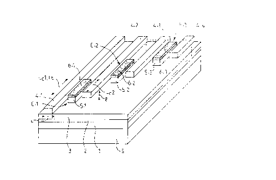
Figure 1 diagrammatically shows a device according to
the invention used in a first application for switching/dis-
tribution of type lx4; and
Figure 2 is a sectional view of the part of the device
in Figure 1 surrounded by dotted lines.
Figures 1 and 2 diagrammatically show an electro-optical
device according to the invention in a first, non-restrictive
embodiment. Here, the electro-optical device forms a
switch/distributor of the ~lx4~ type which enables at least
one output of four outputs to be supplied from one input.
In the following description, the device is constructed
on the basis of a structure formed from a stack of layers
which are preferably made from semi-conductor materials. In
CA 022~4373 1998-11-23
fact, any multilayer structure which makes it possible to
define waveguides which are substantially parallel to one
another, at least in parts, and substantially in the same
plane, may be envisaged provided that electro-optical control
means according to the invention make it possible to control
the transfer of a light wave from one waveguide to another
waveguide.
In the example shown in Figures 1 and 2
the structure compri~es a first confining layer 1,
preferably made from a binary material of the (non-doped)
intrinsic InP type above which is placed a guide layer 2,
preferably made from a quaternary material of the InGaAsP
type lattice-matched to the guide material (in this case
InP), and a second confining layer 3, also preferably made
from a binary material of the intrinsic InP type. A struc-
ture of this kind would not of itself make it possible to
define local (longitudinal) waveguides. To obtain such a
result, the structure comprises, at selected points, here
placed periodically above the second confining layer 3 of
intrinsic InP, "primary" lines 4-i parallel to one another
and preferably made from a binary material of the type used
for the confining layers, namely InP, but in this case p+
doped.
In fact, as is well known to those skilled in the art,
by the local addition of a suitable material (in this case
the primary lines 4-i) above a stack of two confining layers
enclosing a guide layer, the effective optical index is
modified in the region located below the suitable added
material. A lightwave of selected wavelength A may thus be
confined in this region, substantially centred on the guide
layer 2. Thus, straight with each primary line, a waveguide
- _ is defined wherein a lightwave and, more precisely, at least
one first propagation mode thereof is able to propagate.
It is clear that the proportions used for the materials
which constitute the layers and the primary lines, in this
case indium, phosphorus, gallium and arsenic, as well as the
respective thicknesses of the layers and the dimensions of
the primary lines, are selected so as to enable local guiding
of the light wave of selected wavelength A.
CA 022~4373 1998-11-23
As a non-restrictive example, within the scope of
guiding a lightwave of wavelength A equal to 1.55 ~m, the
following thicknesses will be chosen for each layer of the
structure:
- first confining layer 1 of intrinsic InP: 0.6 microns;
- guide layer 2 of InGaAsP (with a gap of 1.15 ym): 0.2 ~m;
- second confining layer 3 of intrinsic InP: 1.5 ~m;
- primary lines 4-i (i = 1 to 4) of p+ doped InP: 0.6 ~m~
Above the primary lines~ 4-i, with a view to optimising
the injection of carriers into the structure and hence
improving ohmic contact, a terminal layer, preferably of a
ternary material of the p+ doped InGaAs type may be provided.
In such a case, and in the example described, this layer is
preferably 0.3 ~m thick.
Moreover, in this example, the width L and height 1 of
each primary line will be substantially equal to 4 ~m and 1.8
~m, respectively, these primary lines 4-i being periodically
spaced from one another by a distance of about 7 ~m.
Preferably, again, in this example, the doping of the
material forming the primary lines 4-i is of the order of
1018, whilst the doping of the material of the terminal layer
of InGaAs is about 1019. The structure described previously
is, again preferably, placed on a substrate S of n+ doped InP.
Preferably, the different layers forming the structure,
namely the confining layers 1 and 3, the guide layer 2 and
the layer from which the primary lines 4-i are formed, are
obtained by growth on a substrate A of InP using an epitaxy
technique, e.g. molecular beam epitaxy (MBE) and more
preferably gas source molecular beam epitaxy (GSMBE).
Of course, other types of growth may be envisaged, such
as for example that obtained by metal-organic chemical vapour
deposition (MOCVD).
It has already been pointed out that it was preferable
for the primary lines to be formed from a "complete" layer
using, for example, a technique of reactive ion etching (RIE)
under oxygen plasma, or by selective chemical attack.
However, it is clear that other techniques may be used such
as for example selective epitaxy. In this case, it is
CA 022~4373 1998-11-23
obviously not appropriate to provide a complete layer for the
primary lines.
The Applicants have noticed that by judiciously placing
an electro-optical control element E-j (j = 1 to 3 in Figure
1) of predetermined dimensions at a location selected between
two adjacent primary lines 4-i and 4-(i+1), it was possible
to transfer a lightwave between the two waveguides defined by
the primary lines 4-i and 4-(i+1). In other words, it is
possible to control the co~plete transfer of the -wave by
providing an all-or-nothing switch, or to control partial
transfer of this wave by providing an energy distributor.
In order to do this, the electro-optical element
E-j must permit local propagation, i.e. propagation in the
region above which it is located, of a second propagation
mode of the lightwave affecting the two adjacent waveguides
together. In fact, as is known to those skilled in the art,
when two modes of propagation of a lightwave coexist in the
same region, coupling of these modes may occur under certain
conditions, inducing physical displacement of the first mode.
20The electro-optical control element E-j must therefore
define, like the primary lines 4-i, but under control, a
local waveguide known as the "transfer" waveguide in the
~ region located below it.
In the embodiment shown in the drawings, the electro-
optical control element E-j is formed from a secondary line
5-j adapted to define a waveguide, like all the primary lines
4-i, at right angles thereto. Preferably, secondary lines 5-
j of this kind are produced at the same time as the primary
lines 4-i and hence using the same technique (etching,
chemical attack or selective epitaxy) and the same materials,
i.e. in the specific example illustrated, p+ doped InP.
The width L and height l of each secondary line 5-j are
substantially identical to those of the primary lines 4-i (in
this example L = 4 ~m and l = 1.8 ~m). By contrast, their
(longitudinal) extent parallel to the primary lines 4-i must
without fail be equal to or greater than a whole number times
the coupling length Lc necessary for effective coupling
between a waveguide defined by a primary line in which the
lightwave circulates and an adjacent waveguide section
CA 022~4373 1998-11-23 ''
defined by a secondary line, which will be used for transfer
to an adjacent waveguide defined by an adjacent primary line.
In fact, this length defines the minimum distance ensuring
that two propagation modes, e.g. symmetrical and antisymme-
trical, which consequently have different propagationvelocities, will be able to be added together constructively.
This coupling length Lc can be determined from equations
of propagation of a light wave and more precisely its
propagation modes. It is giyen by the following formula:
Lc =
2(neven ~ nodd)
where neven and nOdd respectively denote the effective optical
indices of the first and second propagation modes of the
lightwave of wavelength ~ in the waveguide. These two
indices are a function particularly of the materials used to
form the structure, the thicknesses of these materials and
the geometric characteristics of the structure, including the
spacing between waveguides.
It is important to note here that, given that the
distance between a waveguide and the adjacent waveguide
portion influences the coupling length Lc between these two
guides, the first coupling length Lcl between a first guide-
and the adjacent guide portion, and the second coupling
length LC2 between a second guide adjacent to the first (and
with which they enclose the guide portion) and said adjacent
guide portion, will only be equal if said waveguide portion
is arranged so as to be equidistant from the first and second
waveguides.
In the example described in detail above and illustrated
in Figure 1, solely by way of example, the two coupling
lengths Lcl and LC2 are not identical owing to the fact that
the secondary line E-1 defining the waveguide portion is
placed closer to the second primary line 4-2 than to the
first primary line 4-1 (the reasons for this spacing will be
explained hereinafter). Thus, a first coupling length Lcl=LE
of about 800~m is necessary for transferring the first
symmetrical mode of the first waveguide, defined by the first
primary line 4-1, to the transfer waveguide portion, defined
by the first secondary line E-1, whereas a second coupling
CA 022~4373 1998-11-23 - -
length LC2 of about 600 ~m is necessary for the transfer of
the first symmetrical mode of the transfer waveguide portion
(e-1) to the second waveguide, defined by the second primary
line 4-2.
It is clear that the electro-optical element E-j made up
of the sole secondary line 5-j automatically carries out the
virtually integral transfer of the first mode of the wave
from a first guide to a second guide without any need to act
on this electro-optical elempnt. However, if a true switch
or, better still, an energy distributor is desired, it is
necessary for the electro-optical element E-j to prevent the
transfer of the lightwave, totally or partially, and conse-
quently to prevent the coupling of its first and second
modes, from one waveguide to the other.
Preferably, the controlling of the transfer (or cou-
pling) is carried out by controlling the value of the
effective optical indices of the structure in the region
situated below the secondary line 5-j, viewed by the first
and second modes.
To do this, it is particularly useful to inject an
electric current into the secondary line 5-j, possibly a
variable intensity current (if one wishes to produce an-
- -~ energy distributor), or in other words to inject carriers,
e.g. electrons.
To achieve this objective, the upper surface (opposite
the second confining layer 3) of each secondary line 5-j may
be covered with an ohmic contact made of Pt/Ti/Pt/Au, for
example. An ohmic contact deposit may be obtained, for
example, by a method comprising a lithography step followed
by an evaporation step well known to those skilled in the art
and therefore requiring no further description here. The
ohmic contact of each element E-j is thus connected to a
control module which is able to manage their respective power
supplies via ~electric cables", for example. Of course, a
fully integrated device may also be envisaged in which the
control module and the connections are integrated in the
structure.
The injection of carriers into the secondary line 5-j,
when it exceeds a predetermined threshold dependent on the
CA 022~4373 1998-11-23
materials which make up the structure, has the result of
varying the effective optical indices in the region which
extends between the two waveguides where it is located (and
more particularly below), by a value such that the second
mode of the lightwave can no longer be propagated there, thus
preventing any coupling between the first and second modes.
When the intensity of the current injected into a
secondary line 5-j via its ohmic contact 6-j is between zero
and said predetermined thre,shold, it is then possible to
monitor the amplitude of the coupling, so that the light wave
can be distributed in the two guides enclosing the optical
element in question. In this way an energy distributor is
created.
It is clear that when the intensity of the current
injected into the electro-optical modules E-j can only assume
the value zero or a value greater than or equal to the
predetermined threshold, the device operates as an all-or-
nothing switch.
The electrical behaviour of the device or, in other
words, the intensity necessary to control the transfer of a
light wave between two adjacent guides can be deduced by
solving the equations given below:
- - the Poisson equation (1):
~ 2X = Nd-Na+p-n
- equations of the charge-carrying currents (2):
jn = -nVn = lln(nEx+ ,Sx)
+nvp = llp (PEx ~x )
it = jn + jp + ~ E
where the indices n and p denote, respectively, the carriers
of the electron and hole types, n and p are, respectively,
the densities of carriers of the electron and hole types, the
j's denote carrier current densities, v and ~ respectively
denote the velocity and mobility of the carriers;
CA 022~4373 1998-11-23
- and continuity equations (3) :
8n = ~Jn + g - U, and ~t 8x
where g and u respectively denote the generation and recombi-
nation levels (electron-hole) of the carriers;
and where:
8X ~n(P+ni) +Tp(n+ni)
where ni denotes the carrier density in the intrinsic
semiconductor and the ~'s denote the recombination times of
the carriers,
- and by using the HUNSPERGER equation (4) which gives the
carrier density as a function of the variation in the
refractive index :
n - n = -1 N2A2~2
~ 2 nOm~0~2c2
where N denotes the carrier density, q the charge of the
electron, nO denotes the initial optical index before the
- injection of carriers, m* denotes the effective mass of the
electron.
15Using a structure such as the one shown in Figure 1,
which is made up of four waveguides defined by four primary
lines 4-1 to 4-4, and comprising between each pair of
adjacent primary lines an electro-optical control element E-l
to E-3 connected to a control module (not shown), it is then
possible, by injecting a light wave at the inlet to the first
waveguide defined by the first primary line 4-1 (the entrance
being indicated by an arrow) to transfer this light guide
partially or totally from the first waveguide to the second
and/or third and/or fourth, depending on whether carriers are
injected into one or more electro-optical control elements 5-
j and depending on the intensity of the injected current.
Thus, if none of the three electro-optical control elements
E-l to E-3 is supplied with current, the wave injected into
the first guide will re-emerge from the exit of the fourth
CA 022~4373 1998-11-23
guide defined by the fourth primary line 4-4. By contrast,
if only the first secondary line 5-1 is not supplied with
current, but only the second secondary line 5-2 is supplied
with a current greater than or equal to the predetermined
threshold, the lightwave will re-emerge from the exit end of
the second waveguide defined by the second primary line 4-2.
A large number of other cases may be envisaged, depen-
ding on whether the intensity of the supply current to the
electro-optical control ele~ents E-j can be continuously
regulated or whether it is of the binary type. Thus, in the
first hypothesis, where the current intensity is adjustable,
with the device shown in Figure 1 one can envisage delivering
four portions of the light wave which has entered through the
first waveguide, at the four outlets of the four waveguides.
In the example shown in Figure 1, the primary lines 4-i
are not all of identical lengths, owing to the fact that the
device is designed here to operate as a lx4- type switch.
However, it is clear that all the primary lines may be of
substantially equivalent lengths, or else a number of them
may be of a first length and a number of others may be of a
second length, so that a light wave can be injected into the
device at several different locations.
- - In one embodiment in which the four primary lines would
have the same longitudinal extents and wherein one or more
electro-optical control units E-j would be placed between
each pair of primary lines 4-i, a 4x4 energy distributor
could be produced, each entrance to the waveguides being
capable of receiving the lightwave.
However, it is important to note that, with a view to
obtaining a device in which the switching is ~'two-way~, i.e.
switching is possible from a first guide to a second and from
the second to the first, it is preferable, if one wishes to
use only one control element E-j (transfer guide), to place
the secondary line at an equal distance from the two primary
lines which enclose it.
However, such positioning has the disadvantage of
creating crosstalk and consequently signal loss. To prevent
this, it would be preferable locally to bend one of the two
primary lines which enclose a secondary line just after this
CA 022~4373 1998-11-23
secondary line (and hence at the exit from the coupling
zone), so that the two primary lines are spaced from one
another. In other words, it is sufficient for the lines to
be parallel to one another along the coupling length.
Nevertheless, in the structures where such symmetry is
unnecessary, i.e. when switching need occur only in one
direction, always the same one, it is preferable for the
secondary line 5-j to be closer to the primary line 4-(i+l)
into which the lightwave is~to be transferred than to the
primary line 4-i wherein the lightwave to be transferred
circulates. This makes it possible to improve the transfer
and limit the crosstalk effects as far as possible.
This asymmetrical positioning of the secondary lines 5-j
is better illustrated in Figure 2 which shows the cross
sectional view of the structure at the part which is enclosed
by dotted lines in Figure 1.
In the example described in detail hereinbefore, the
Applicants have found that it was advantageous for the
secondary line 5-j to be twice as close to the primary line
4-(i+l) of the "receiver" guide than to the primary line 4-i
of the "transmitter" guide. In fact, the optimum spacing of
each of the two primary lines can be calculated from the
above equations, in particular. These spacings depend
chiefly on the amplitude of the optical confinement induced
by the presence of the primary and secondary lines and
consequently by their height 1. For example, again with
reference to the device described in detail hereinbefore, the
value chosen for the first spacing 11 will be about 2~m and
the value for the second spacing 12 will be about 1 ~m.
It is clear that numerous alternative embodiments of the
device described may be envisaged. Thus, several (at least
two) transfer control elements (E-j) may be placed between
one or more pairs of adjacent primary lines 4-i and 4-(i+l)
so that one or more lightwaves can be transferred from one
guide to the other and vice versa. Without doubt, an
embodiment of this kind requires a plurality of primary lines
extending over the full length of the device, so that the
wave or waves can be introduced into the structure at several
points. This would make it possible, for example, to mix the
. ~
CA 022~4373 1998-11-23
lightwave coming from a first waveguide with a second
lightwave coming from another waveguide.
The invention is not restricted to- the embodiments
described hereinbefore with reference to the drawings, but
covers all the alternatives which might be developed by the
skilled person within the scope of the claims which follow.
Thus, the number and dimensions of the waveguides as
well as the number and positions of the various electro-
optical control means may v~ry depending on the particular
application.
Furthermore, a device is described in which only one
layered structure was provided, but it is plain that it would
be possible to superimpose a number of structures on one
another, e.g. by burying the primary and secondary lines
using suitable material, so as to form a multi-level device
with a high degree of integration.
Moreover, a device is described in which the materials
which form the layers of the structure were semiconductors,
but plainly the invention is not limited to these materials
alone. Thus, one might envisage the use of polymers such as
PMMA or PMGI or even dielectric materials such as SiO2.
Finally as indicated above, it would be possible to
superimpose a number of structures the respective materials
of which were not identical from one structure to the next,
in order to allow the treatment (switching/distribution) of
lightwaves of different wavelengths.