Note : Les descriptions sont présentées dans la langue officielle dans laquelle elles ont été soumises.
CA 02254651 1998-11-26
AT9-97-284
METHOD AND APPARATUS FOR COUPLED PHASE LOCKED LOOPS
BACKGROUND OF THE INVENTION
1. Technical Field:
The present invention relates in general to integrated circuit technology. In
particular, the present
invention relates to clock generation devices, such as utilized in CMOS
microprocessor integrated
circuits.
2. Description of the Related Art:
In the design of integrated microprocessor circuits utilizing dynamic
circuits, it is highly desirable
to employ circuits having low fitter. "litter" is a vibration or fluctuation
in a signal. In integrated
circuit devices in particular, fitter is often the result of supply noise and
substrate noise, and is seen
as short-term instabilities in either the amplitude or phase of a signal.
litter can thus be described
as uncertainty in the occurrence of a clock edge. Two types of fitter,
negative fitter and positive
fitter, are usually encountered in integrated circuit devices. Negative fitter
is the amount of time a
clock edge precedes its ideal time. Positive fitter is the amount of time a
clock edge lags its ideal
time. Negative fitter of clock sources detracts from the usable cycle time of
microprocessor systems.
As one example of the importance of fitter, for high-resolution graphic
display devices utilizing
phase-locked loop designs, the fitter performance of phase-locked loops limits
the system
performance. (A phase-locked loop ("PLL") is a circuit or system that utilizes
feedback to maintain
an output signal in specific phase relationship with a reference signal.)
Power-supply noise coupling
is a major cause of fitter problems seen in such PLL's, especially with low-
supply voltages and with
multiple clock synthesizers on the same device.
The utilization of PLL's for generating microprocessor clocks is well known in
the art of integrated
circuit design. For PLLs located on the same chip as a high-performance
microprocessor, the power
CA 02254651 1998-11-26
AT9-97-284 2
supply switching noise of the digital circuits is a major noise source for
output fitter. For low-power
PLLs, a second fitter source is the intrinsic noise of metal-oxide silicon
devices in the PLL voltage
controlled oscillator. This noise can be reduced by increasing power
consumption. To obtain
low-voltage analog circuits, the saturation voltage of MOS devices must be
reduced by utilizing
wider devices, which results in a larger parasitic capacitance between the
supply voltage and the
analog nodes. This larger parasitic capacitance decreases the power supply
noise rejection for the
same current consumption. Thus, a challenge in utilizing PLL's for
microprocessor clock generation
is to design a PLL which combines limited fitter, low-supply voltage and low-
power consumption.
Despite improvements in PLL based system fitter, the above described problems
present difficulties
in their application.
Surface acoustic wave ("SAW") oscillators would seem attractive for PLL
applications, since SAW
oscillators operate at very high frequencies and are manufactured to meet
precise frequency
specifications, such as having fitter of only 10 picoseconds, for example.
However, a conventional
analog PLL includes a voltage controlled oscillator (VCO) with a relatively
large fitter, such as 200
picoseconds, for example. In combining a Surface Acoustic Wave ("SAW")
oscillator with a
conventional PLL, the relatively the large fitter of the PLL voltage
controlled oscillator adds to the
much smaller fitter of the SAW.
One or more of the above referenced, copending applications discloses a SAW
oscillator combined
with a digital locked loop instead of the more conventional analog PLL. The
term digital locked
loop ("DLL"), as used to apply to the inventions disclosed herein and in the
related applications, is
different than a conventional DLL. Generally, the term "DLL" as used in the
conventional sense
and as used herein, refers to a special type of phase locked loop. Like any
phase locked loop, the
DLL includes circuitry for generating a periodic signal and for phase
adjusting the signal based on
a feedback signal. The feedback signal is derived, in part, from the periodic
signal itself. In a
conventional DLL there is a digital delay element within the feedback path -
that is, a delay element
for which the delay is adjusted in discrete steps controlled by the logical
state of digital logic
CA 02254651 1998-11-26
AT9-97-284 3
elements. This digital delay element is used for phase adjustment. For more
background, see, for
example, U.S. patent numbers 5,442,776 and 5,610,548. In the DLL of the
present and related
inventions, the phase adjustment is controlled digitally, but not by merely
varying a digital delay
element.
S
For an on-chip clock application, the digital-locked loop incorporating a SAW
oscillator, as
disclosed in the above referenced co-pending application, reduces negative j
fitter to approximately
picoseconds, based on an inherent operating fitter of 0.4% for a 400 MHz
machine cycle. In
comparison, a conventional analog PLL has negative fitter of approximately 200
picoseconds, based
10 on a fitter of 8% for a 400 MHz machine cycle.
Positive fitter, on the other hand, is allowed to occur infrequently for the
SAW/DLL combination,
even to the extent of hundreds of picoseconds. However, because the positive
fitter occurs so
seldom, and the fundamental frequency of the SAW oscillator may be specified
with such precision,
the positive fitter is of no consequence for on-chip clock sources. That is,
the resulting long-term
frequency of the clock is stable at 400 MHz for on-chip applications.
While replacing a conventional PLL with a SAW-based, digital-locked loop in
accordance with the
above referenced patent application substantially improves the fitter for an
internal chip clock,
nevertheless, additional problems remain for chip-to-chip interfaces. An
asynchronous chip-to-chip
interface would be an alternative to deal with these problems, but
metastability problems of such
asynchronous interfaces are conventionally solved by pipelined latches to
resynchronize data. Such
latches introduce extra latency which may be unacceptable.
Thus, a need exists to reduce positive fitter penalties associated with chip-
to-chip paths for
DLL/SAW based clocks.
CA 02254651 1998-11-26
AT9-97-284 4
SUMMARY OF THE INVENTION
It is therefore an object of the present invention to address the foregoing
need. More generally, it
is an object of the present invention to provide a clock generation device
broadly useful for high
speed microelectronic devices. The above and other obj ects are achieved as is
now described.
A first form of the invention encompasses a method for generating synchronized
clock signals.
According to this form of the invention, first and second pluralities of
signals are generated, having
time-varying phase differences with respect to a reference clock. The first
clock is supplied by a
succession of signals from among the first plurality of signals, in which one
of the signals succeeds
another responsive to a first phase difference. The second clock is supplied
by a second succession
of signals from among the second plurality of signals. One signal in the
second succession of signals
succeeds another responsive to a second phase difference. The succession among
the first plurality
of signals is also responsive to the second phase difference.
In other aspects, the succession among the first plurality of signals
responsive to the second phase
difference is for the second phase difference being in a first direction.
Additionally, the switching
among the second plurality of signals responsive to the second phase
difference is for the second
phase difference being in a second direction.
In further aspects, the first phase difference is a phase difference between
the first clock and the
reference clock. The second phase difference is a phase difference between the
first and second
clocks.
In another form, the invention encompasses an apparatus for generating
synchronized clock signals.
According to this form, the invention includes a generating means for
generating first and second
pluralities of signals, having time-varying phase differences with respect to
a reference clock signal.
It also includes first synchronizing means, responsive to a first phase
difference, for supplying a first
clock by a first succession of signals from among the first plurality of
signals, and second
synchronizing means, responsive to a second phase difference, for supplying a
second clock by a
CA 02254651 1998-11-26
AT9-97-284 5
second succession of signals from among the second plurality of signals. The
first synchronizing
means is also responsive to the second phase difference.
In further aspects, the first synchronizing means is responsive to the second
phase difference being
in a first direction. Also, the second synchronizing means is responsive to
the second phase
difference being in a second direction. Further, the first phase difference is
a phase difference
between the first and reference clock signals. In addition, the second phase
difference is a phase
difference between the first and second clock signals.
BRIEF DESCRIPTION OF THE DRAWINGS
The novel features believed characteristic of the invention are set forth in
the appended claims. The
invention itself, however, as well as a preferred mode of use, further objects
and advantages thereof,
will best be understood by reference to the following detailed description of
an illustrative
embodiment when read in conjunction with the accompanying drawings, wherein:
FIG.1 is a pictorial representation of a data-processing system which may
utilize the system
and method of the present invention;
FIG. 2 depicts a block diagram illustrative of selected components in a
personal computer
system which may utilize the system and method of the present invention;
FIG. 3 is a high-level block diagram illustrative of a self synchronizing
phase delay system
for coupling digital-locked loops in accordance with a preferred embodiment of
the present
invention;
FIG. 4 is a more detailed block diagram illustrative of a self synchronizing
phase delay
system for coupling digital-locked loops in accordance with a preferred
embodiment of the present
invention;
FIG. 5 is a diagram of phase error versus time, for a single digital-locked
loop using a
surface acoustic wave oscillator.
FIG. 6 is a diagram of phase error versus time for coupled digital-locked
loops in
accordance with the system of FIG. 4.
CA 02254651 1998-11-26
AT9-97-284 6
DETAILED DESCRIPTION OF PREFERRED EMBODIMENT
With reference now to the figures and, in particular, with reference to FIG.
1, there is depicted a
pictorial representation of a data-processing system in which the present
invention may be
implemented in accordance with a preferred embodiment of the present
invention. The
data-processing system includes a personal computer 10 in which are
implemented a system unit 12,
a video display terminal 14, an alphanumeric input device (i.e., keyboard 16)
having alphanumeric
and other keys, and a mouse 18. An additional input device (not shown), such
as a trackball or
stylus, also can be included with personal computer 10. Computer 10 can be
implemented utilizing
any suitable computer, such as an IBM Aptiva computer, a product of
International Business
Machines Corporation, located in Armonk, N.Y. "Aptiva" is a registered
trademark of International
Business Machines Corporation.
Although the depicted embodiment involves a personal computer, one skilled in
the art will
appreciate that a preferred embodiment of the present invention may be
implemented in other types
of data-processing systems, such as, for example, intelligent workstations or
mini-computers.
Computer 10 also preferably includes a graphical user interface that resides
within a
machine-readable media to direct the operation of computer 10. Computer 10
also can be
implemented utilizing any suitable computer, such as the IBM RISC/6000
computer, a product of
International Business Machines Corporation, located in Armonk, N.Y. "RISC
SYSTEM/6000" is
a trademark of International Business Machines Corporation, and also can be
referred to as the
"RS/6000."
Referring now to FIG. 2 there is depicted a block diagram of selected
components in personal
computer 10 of FIG. 1 in which a preferred embodiment of the present invention
may be
implemented. Personal computer 10 of FIG. 1 preferably includes a system bus
20, as depicted in
FIG. 2. System bus 20 is utilized for interconnecting and establishing
communication between
various components in personal computer 10. Microprocessor or central
processing unit (CPU) 22
is connected to system bus 20 and also may have numeric co-processor 24
connected to it. Direct
CA 02254651 1998-11-26
AT9-97-284 7
memory access ("DMA") controller 26 also is connected to system bus 20 and
allows various
devices to appropriate cycles from CPU 22 during large input/output ("I/O")
transfers.
Read-only memory ("ROM") 28 and random-access memory ("RAM") 30 are also
connected to
system bus 20. ROM 28 is mapped into the microprocessor 22 address space in
the range from
640K to 1 megabyte. CMOS RAM 32 is attached to system bus 20 and contains
system-configuration information. Any suitable machine-readable media may
retain the graphical
user interface of computer 10 of FIG. 1, such as RAM 30, ROM 28, a magnetic
diskette, magnetic
tape, or optical disk.
Also connected to system bus 20 are memory controller 34, bus controller 36,
and interrupt
controller 38 which serve to aid in the control of data flow through system
bus 20 between various
peripherals, adapters, and devices. System unit 12 of FIG. 1 also contains
various I/O controllers,
such as those depicted in FIG. 2: keyboard and mouse controller 40, video
controller 42, parallel
controller 44, serial controller 46, and diskette controller 48. Keyboard and
mouse controller 40
provide a hardware interface for keyboard 50 and mouse 52.
Video controller 42 provides a hardware interface for video display terminal
54. Parallel controller
44 provides a hardware interface for devices such as printer 56. Serial
controller 46 provides a
hardware interface for devices, such as a modem 58. Diskette controller 48
provides a hardware
interface for floppy-disk unit 60. Other technologies also can be utilized in
conjunction with CPU
22, such as touch-screen technology or human voice control.
Expansion cards also may be added to system bus 20, such as disk controller
62, which provides a
hardware interface for hard-disk unit 64. Empty slots 66 are provided so that
other peripherals,
adapters, and devices may be added to system unit 12 of FIG.1. A network card
67 additionally can
be connected to system bus 20 in order to link system unit 12 of FIG. 1 to
other data-processing
system networks. Those skilled in the art will appreciate that the hardware
depicted in FIG. 2 may
CA 02254651 1998-11-26
AT9-97-284 8
vary for specific applications. For example, other peripheral devices, such
as: optical-disk media,
audio adapters, or chip-programming devices, such as PAL or EPROM programming
devices and
the like also may be utilized in addition to or in place of the hardware
already depicted. Note that
any or all of the above components and associated hardware may be utilized in
various
embodiments. However, it can be appreciated that any configuration of the
aforementioned system
may be utilized for various purposes according to a particular implementation.
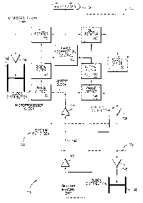
In FIG. 3 and FIG. 4, like parts are indicated by like numbers. FIG. 3 is a
high-level block diagram
illustrative of a self synchronizing phase delay system 100 for coupling DLL's
in accordance with
a preferred embodiment of the present invention. System 100 is a self
synchronizing phase delay
system for coupling DLL's , which causes phase adjustments of the digital-
locked loops to occur
simultaneously at a synchronization point.
System 100 reduces the timing penalty for misaligned phase adjustment normally
associated with
independently operating DLL's. The normal penalty increases chip-to-chip path
time. In the
configuration of FIG. 3, a SAW oscillator 104 sends a first reference signal
to microprocessor chip
102, which also receives a second reference signal from system bus clock 106.
An off chip memory
chip 108 is coupled to microprocessor 102, which is also coupled to a system
bus 110.
Microprocessor chip 102 is the physical realization of a CPU of a given
computer system on either
a single semiconductor chip or on a small number of chips. For example,
microprocessor chip 102
can be a CPU such as CPU 22 depicted in FIG. 2.
Microprocessor chip 102 can also be included as part of a mufti-chip
microprocessor system, such
as mufti-chip uniprocessors, uniprocessors with off chip memory, or
multiprocessor configurations.
A first reference signal, system bus clock 106, is provided to microprocessor
chip 102 via bus lines.
SAW oscillator 104 provides a second reference signal. SAW oscillator 104 can
be a crystal
oscillator based on an appropriate oscillation producing material such as
quartz crystals. Off chip
memory chip 108 can provide extra memory, such as a cache memory area, for
utilization with
CA 02254651 1998-11-26
AT9-97-284 9
microprocessor chip 102. Together, microprocessor 102 and off chip memory chip
108 provide the
basis of a multiprocessor.
FIG. 4 is a more detailed block diagram illustrative of a self synchronizing
phase delay system 112
for coupling DLL's in accordance with a preferred embodiment of the present
invention. Details
of the various functional blocks of FIG. 4. are described in the above
referenced and incorporated,
co-pending applications. SAW oscillator 104 is preferably an 800.4 MHz SAW
oscillator.
Microprocessor chip 102 includes a first DLL rotator 118 which receives the
second reference signal,
i.e., the signal from SAW oscillator 104. A second DLL rotator 116 also
receives the signal from
SAW oscillator 104.
The rotators 116 and 118 generate a number of signals in response to the SAW
oscillator input
signal, which are used in turn as a source signal for a clock. In the
embodiment described herein
below in connection with FIG. 5, four signals are generated by such a rotator.
The first such signal
generated by such a rotator leads the second signal by 1 /4 cycle, the second
signal leads the third by
1/4 cycle, and the fourth signal leads the third by 1/4 cycle. One of the four
signals is selected as
a source signal at a time for output by such a rotator. Furthermore, the
selection of source signals
goes in sequence, wherein the second signal is selected following the first,
the third signal is selected
following the second, and so on. Hence, the term "rotate" is used to refer to
a change in the selected
source for the output signal from such a rotator, since the selection rotates
among the four possible
source signals in the 1-2-3-4-1-etc. sequence. And the term "stall" is also
used to refer to such a
change in the selected source signal for outputting from such a rotator, since
each of the four signals
is 1 /4 cycle behind the preceding signal, so that switching from the first
signal to the second, and so
forth substantially instantaneously introduces a 1/4 cycle shift in the
rotator output in a lagging
direction.
First DLL rotator 118 provides a first clock signal to clock divider 130,
which reduces the frequency
of the first clock signal by a predetermined multiple, such as by a multiple
of two, to provide a
CA 02254651 1998-11-26
AT9-97-284 10
"memory clock" signal, i.e., a clock signal for off chip memory.
Second DLL rotator 116 sends a second clock signal to buffer 126, which in
turn provides the
buffered clock signal to clock distribution system 1Z8. Clock distribution
system 128 distributes the
buffered clock signal (the "microprocessor clock" signal) throughout the
distribution system 128.
Output from phase correction control circuit 120 is input to first DLL rotator
118 and second DLL
rotator 116. A control signal from second phase detector 132 is fed to second
digital filter 122.
A control signal from second digital filter 122 is fed to phase correction
control circuit 120. A
control signal from first phase detector 134 is fed to first digital filter
l24. A control signal from
first digital filter 124 is also fed to phase correction control circuit 120.
Second phase detector 132 receives the second clock signal from DLL Rotator
116 via clock
distribution 128. First phase detector 134 receives the first reference signal
from system bus clock
106. Buffer 136 provides the clock signal from divider 130 to second phase
detector 132 and first
phase detector 134.
Off chip memory chip 108 includes a buffer 142 which receives the clock signal
from divider 130,
via buffers 138 and 146. Output from buffer 146 is also coupled to clock
distribution system 148.
System 112 allows first and second clock signals from first and second DLL
rotators 118 and 116
to be placed under coordinated control. That is, the first and second clock
signals are fed back,
including through the clock distribution path 128 and interchip paths (between
the microprocessor
and the off chip memory), to control circuitry, so that the first and second
clock signals can be
synchronized to each other and the system bus clock 106.
The system bus clock and memory clock are phase locked as follows. First phase
detector 134
detects a phase difference between the system bus clock and the memory clock,
derived from the
CA 02254651 1998-11-26
AT9-97-284 11
first clock as divided by bus divider 130 and delayed by interchip paths, and
provides a control
signal responsive to the measured phase error to digital filter 124. The first
digital filter integrates
the error signal and provides a control signal responsive thereto to the phase
correction control
circuitry 120, which controls stalling of the memory clock signal by the first
rotator 118.
The microprocessor clock and memory clock are synchronized by rotating the
source for the
microprocessor clock each time a source for the memory clock also undergoes a
rotation. That is,
second phase detector 132 detects a phase difference between the
microprocessor clock (i.e., DLL
rotator 116 output) and the memory clock (i.e., DLL rotator 118 output) and
provides a control
signal responsive to the phase difference (i.e. error signal) to digital
filter 122. This second digital
filter 122 integrates the error signal and provides a control signal
responsive thereto to the phase
correction control circuitry l20, which controls stalling of the second (i.e.
microprocessor) clock
signal by the second rotator 116. The net effect on DLL rotator 116, of the
control by phase detector
132, digital filter 122, and phase correction control circuitry 120, is that
the microprocessor clock
signal, i.e., output from DLL rotator 116, undergoes a rotation in response to
rotations of the
memory clock signal, i.e, output from DLL rotator l18, since a rotation (i.e.,
stall) of the memory
clock signal will cause the microprocessor clock to lead the memory clock, and
this will be corrected
through phase detector 132, etc.
If, on the other hand, the memory clock gets ahead of the microprocessor
clock, phase correction
control circuitry 120 causes the memory clock rotator 118 to stall in response
to the error signal from
the microprocessor clock phase detector 132.
Phase correction control by circuitry 120 triggering a rotation of memory
clock DLL rotator 118, in
response to microprocessor-clock-versus-memory-clock-phase-detector 132, need
only be performed
at a low frequency (e.g., 1 kHz), which is fast enough to account for ambient
thermal changes in the
clock propagation loops.
CA 02254651 1998-11-26
AT9-97-284 12
From the foregoing, it can be appreciated that the memory clock signal derived
from the SAW
oscillator and reduced in frequency by divide circuitry 130, is designed to be
slightly faster than the
system bus clock 106. Moreover, the SAW oscillator 104, DLL rotator 118,
divide circuitry 130,
signal paths, phase detector 134, digital filter 124 and phase correction
controller 120 form a first
DLL which stalls the memory clock as required so that the memory clock remains
synchronized with
the system bus clock. In this first DLL, the rotator 118 generates a first
plurality of signals, in
response to the first reference signal from the SAW oscillator. The first
plurality of signals have
time-varying phase differences with respect to the second reference clock
signal from the system bus
clock.
Also, the SAW oscillator 104, DLL rotator 116, microprocessor clock paths,
including distribution
128, phase detector 132, digital filter 122 and phase correction controller
120 form a second DLL
which stalls the microprocessor clock responsive to the microprocessor clock
leading the memory
clock. This synchronizes the memory clock and the microprocessor clock when
the microprocessor
clock leads the memory clock. In this second DLL, the rotator 116 generates a
second plurality of
signals, in response to the first reference signal from the SAW oscillator.
The second plurality of
signals have time-varying phase differences with respect to the second
reference clock signal from
the system bus clock.
All of the above mentioned elements of both DLL's, except phase detector 134
and digital filter 124,
form a third DLL which stalls the memory clock responsive to the
microprocessor clock lagging the
memory clock. This synchronizes the memory clock and the microprocessor clock
when the
microprocessor clock lags the memory clock.
It is helpful to consider timing details of a single DLL, in accordance with
the above described
co-pending applications, before considering such details for the coupled DLL's
described herein
above. In FIG. 5, clock phase error is shown as a function of time for a
single DLL using a SAW
oscillator. This example depicts a desired 400 MHz clock signal. Therefore,
the phase error shown
CA 02254651 1998-11-26
AT9-97-284 13
is a phase error relative to the desired 400 MHz target frequency.
In this example, four possible source signals are derived from the 800.4 MHz
SAW oscillator signal,
wherein the second signal is 1/4 phase behind the first signal, the third
signal is 1/4 phase behind the
second signal, etc. Initially the first possible source signal is used as the
source signal for the desired
400 MHz clock signal. The source for the clock signal is switched from the
first possible source
signal to the second possible source signal, from the second to the third, and
so on. The phase error
shown in FIG. 5 is generated by the selected source signal, and, as previously
stated, is measured
with respect to the target 400 MHz clock signal. That is, during the first
interval shown, from t0 to
tl, the source signal depicted is from the first possible source signal;
during the second interval
shown, from t 1 to t2, the source signal depicted is from the second possible
source signal; etc.
Beginning at time t0 in FIG. 5, the depicted 400.2 MHz source signal creeps
ahead of the desired
400 MHz target by 0.2/400 of the desired cycle for each cycle of the source.
Since one cycle at 400
MHz = 2500 psec, this is shown in FIG. 5 as a phase error increasing in time
with a slope of 0.2/400
* 2500 psec per cycle, i.e. a slope of l .25 pseclcycle. In addition, it is
typical for a SAW oscillator
in this fundamental frequency range to have a total operating fitter of 10
psec. Therefore, FIG. 5
shows the 1.25 psec/cycle phase error slope as a band, 10 psec wide.
Operating at the 400.2 MHz frequency, after 500 cycles the signal derived from
the SAW
oscillator gains 1/4 cycle, with respect to the target 400 MHz. That is, 1/4
cycle = (0.2/400
increasing phase error per cycle) * (500 cycles). In response to reaching the
phase error of 1 /4 cycle,
which ideally occurs at time tl, the source signal is switched from the first
possible source signal
to the second. Since the second possible source signal is 1/4 phase behind the
first, at 400.2 MHz,
this introduces a substantially instantaneous positive shift in phase error
very slightly less than 1 /4
cycle, i.e. a (400/400.2)/4 positive shift in phase error, so that the
accumulated negative phase error
is completely offset to within a margin much smaller than the inherent
operating fitter. Ideally the
switch will be made in response to slightly less than the 1 /4 cycle
accumulated phase error, so that
the positive shift in phase error even more precisely matches the accumulated
negative phase error;
CA 02254651 1998-11-26
AT9-97-284 14
however, for the purpose of illustration in FIG. S, the switching is shown to
occur at 500 cycles for
an accumulated 1 /4 cycle negative phase error, and the correction is
nevertheless shown to exactly
offset the accumulated phase error.
Stated in terms of positive and negative fitter, in addition to 10 psec
uncontrolled positive fitter
arising from the 10 psec operating fitter inherent in the stepped down SAW
oscillator signal, once
every 500 cycles 625 psec positive fitter is intentionally introduced by
switching to a 1/4 phase
lagging signal. As to negative fitter, in addition to 10 psec uncontrolled
negative fitter also arising
from the inherent 10 psec operating fitter, l.25 psec negative fitter per
cycle is intentionally
accumulated over an interval of 500 cycles due to the intentional
specification of a fundamental
frequency derived from the SAW oscillator being 0.2 MHz faster than the
desired 400 MHz clock
signal.
After switching from the first possible source signal to the second, at time
tl, the negative phase
error again begins accumulating at the same rate of 0.2/400 cycles/cycle.
Then, ideally at time t2,
after again gaining 1 /4 cycle, the source signal switches again to the third
possible source signal,
which is 1/4 cycle behind. This process continues repeating in rotation,
switching from the third to
the fourth possible source signal, from fourth to the first, and so on.
It should be appreciated that averaged over 500 cycles, the above described,
single DLL/SAW
oscillator in the above example reduces fitter to about 8.75 psec average
positive fitter and 11.25
psec average negative fitter, including the inherent 10 psec operating fitter.
Furthermore, since it is
well known to manufacture SAW oscillators to a fundamental frequency tolerance
of 500 ppm, the
separation between the target clock frequency (i.e., 400 MHz in the example)
and the source
frequency (i.e., 400.2 MHz in the example) could be reduced to less than the
0.2 MHz separation
used in the example. This would reduce average fitter even further.
It should thus be appreciated that average fitter can be reduced to a value
approaching the inherent
CA 02254651 1998-11-26
AT9-97-284 1 S
operating fitter for a single DLL/SAW oscillator based clock as described
above. Nevertheless, the
relatively infrequent, but large positive instantaneous fitter for such a
clock still poses a significant
limitation for applications where independent DLL/SAW oscillator clock sources
are coupled but
where the intentionally introduced fitter is not synchronized, since the
maximum unsynchronized
instantaneous fitter of two clock signals limits usable cycle time when data
is transferred from a
device timed by of one of the clocks to a device under the timed by the other
clock. That is,
available cycle time is limited by the latest launch time by the device
sending data and the earliest
capture time by the device receiving data. Latest launch time is determined by
the maximum
instantaneous positive phase error of the clock for the launching device,
where the error is not
synchronized with that of the receiving device. Earliest capture time is
determined by the maximum
instantaneous negative phase error of the clock for the receiving device,
where the error is likewise
not synchronized. Thus, for 400.2 MHz DLL/SAW oscillators sourcing 400 MHz
clock on
respective sending and receiving devices, per the maximum instantaneous fitter
values derived in the
above example, the usable cycle time will not even be as much as 0.75 cycle.
FIG. 6 depicts phase errors for the coupled memory clock and microprocessor
bus clock which are
synchronized as described in connection with FIG. 4. Specifically, the
intentionally introduced,
increasing negative phase error, and instantaneous, though infrequent positive
j fitter, introduced once
each 500 cycles, are synchronized for the two clock signals, so that their
effect is not cumulative
with respect to launching and capturing data in transfers between the
microprocessor and memory.
Therefore, only the inherent operating fitter, assumed to be 10 psec, plus the
intentionally introduced
constant I.25 psec/cycle negative fitter reduces the cycle time available for
such data transfers.
Thus, the effective cycle time is reduced by only 11.25 psec
This is illustrated in FIG. 6, for example at a time, ta, when a signal is
launched from a
microprocessor clocked by the microprocessor clock to the memory clocked by
the memory clock.
Suppose the intentionally introduced phase error, ea, of the microprocessor
clock at time to is -100
psec, so that taking into account the 10 psec operating j fitter, the phase
error is in the range -95 to
-105 psec. The phase error for the memory clock at time to is in the same
range, since the
CA 02254651 1998-11-26
AT9-97-284 16
intentionally introduced phase error is synchronized with that of the
microprocessor clock. The
memory clock, however, will capture the signal one cycle after the
microprocessor launched it.
Thus, the memory clock will have an intentionally introduced phase error, eb,
at the time of capture
which will be -101.25 psec, due to the intentionally introduced -1.25 psec
phase error/cycle. The
range of phase error for the memory clock at capture, therefore, taking into
account operating fitter,
will be -96.25 to 106.25 psec. The worst case difference between phase error
at launch and at
capture, will therefore be the difference between -95 psec and -106.25 psec
phase error, i.e., 11.25
psec. It should be appreciated that since the intentionally introduced phase
error is synchronized for
the two clocks, the result will be the same regardless of the choice of time
ta. On the other hand, if
the intentionally introduced phase error was not thus synchronized, ea and eb
would not necessarily
be only 1.25 psec apart for any launch time ta, so the maximum possible phase
error difference and
possible accompanying cycle time loss could be as great as 635 psec, in this
example.
While the invention has been particularly shown and described with reference
to a preferred
embodiment, it will be understood by those skilled in the art that various
changes in form and detail
may be made therein without departing from the spirit and scope of the
invention.