Note : Les descriptions sont présentées dans la langue officielle dans laquelle elles ont été soumises.
I . I
CA 02255512 2002-10-25
78793-1
1
BALLAST FOR DISCHARGE LAMP
Background of the Invention
Field of the Invention
This invention relates to a circuit operation mode
and control thereof suitable for igniting a high intensity
(high pressure) discharge lamp without failure and at low
cost and with low stresses on the circuit. The lamp is
ignited by high frequency voltage and operated by a low
frequency waveform.
Description of Prior Art
In conventional electronic ballasts, specifically
pulse started metal halide discharge lamp ballasts, an extra
ignitor circuit is required. The ignition pulse amplitude
specified by the lamp manufacturer is very high though it
varies among manufacturers. Also, the width of the pulse
has a minimum required value, typically 1.5 microseconds to
2.5 microseconds. To meet the starting pulse requirement,
the ignitor may be complicated and expensive.
In U.S. Patent No. 5,932,976 (see Figs. 1 and 5),
a high frequency resonant ignition technique was described.
This scheme operates the lamp using a high frequency
starting operation and a low frequency steady state
operation alternately (Figs. 2 and 3 or Figs. 6 and 7).
When this circuit is operated in the high frequency starting
mode, a 50~ duty-cycle high frequency square waveform is
applied to the resonant circuit formed by the inductor and
capacitor producing a high voltage to ignite the lamp.
After the detection of lamp ignition, the switching mode
changes to a low frequency stead-state operation. When the
CA 02255512 2002-10-25
78793-1
la
operating mode is changed from the starting operation to the
steady-state operation, there is a delay time (as shown in
Fig. 4 and 8) which is caused by the filtering circuit of
the detecting circuit.
CA 02255512 1998-12-11
- 2 -
This delay time causes instability of the discharge
during the transition from the glow to the arc and the
lamp may be extinguished easily. This phenomenon
frequently happens when the lamp is not cooled down
completely. In the circuit topology, the power control
stage and the inverter stage are combined in a half-
bridge/full-bridge topology. Since the power control
(buck) stage is combined with the output inverter and the
power circuit is working in discontinuous current mode at
steady state operation, in order to prevent acoustic
resonance, the output inductor and the capacitor across
the lamp must provide sufficient filtering to keep the
high frequency component of the lamp current to a
minimum. Consequently, the value of the capacitor must
be large, in the order of 1/10 micro farads. Because of
the large capacitance value and relatively small inductor
value, very large circulating current flows in the
circuit during high frequency starting operation.
In U.S. Patent No. 5,182,702, a control scheme of
unbalanced duty-cycle operation for a dimming control is
described. The unbalanced duty-cycle operation control
allows the ballast output current to stably be controlled
at a fixed switching frequency.
Summary of the Invention
The present invention overcomes the disadvantages
of the above-mentioned technique and keeps the advantage
of high frequency starting. The objective of the
invention is to overcome the problems of the lamp
extinguishing due to the delay time and the high
circulating current in the prior art. Another objective
of the invention is to simplify the circuit for igniting
HID lamps and reduce the cost of the HID ballast.
The circuit of the present invention utilizes a
half bridge (shown in Fig. 9) or a full bridge (shown in
CA 02255512 1998-12-11
- 3 -
Fig. 12) inverter circuit to provide the HID lamp with
low frequency current. The inverter also controls the
lamp power and current. In the new igniting control
scheme, at starting mode, the duty-cycle of the switches
is modulated by the required output low frequency square
waveform or a fixed amplitude DC signal and the voltage
on the lamp is composed of the high frequency, high
voltage plus the low frequency square waveform voltage or
DC voltage as shown in Figs. 11, 14, and 16. It is the
high frequency, high voltage that breaks down the lamp
and it is the low frequency square waveform voltage or DC
voltage that pushes the lamp from the glow to the arc as
the lamp is broken down. In this way, the lamp current
can be set up in no delay time and then the lamp current
is controlled by the current loop. Therefore the lamp
can be ignited without failure.
In the inverter, during the steady-state, the
current in the output inductor, which is a buck inductor,
is continuous. There are separate current and voltage
loops in the control circuit to control the lamp power
and the lamp current. The current in the output inductor
can be considered as a controllable current source. Due
to the continuous current of the output inductor, the
current ripple is low. Because of the low ripple on the
output current, it isn't necessary to use a second order
filter formed by the output inductor and the capacitor
parallel with the lamp to filter out the high frequency
ripple current through the lamp to avoid acoustic
resonance. In this case, the value of the capacitor
parallel with the lamp will be determined by the lamp
ignition. Due to the low value of the capacitor, it is
possible to make the resonant tank circulating current as
low as possible and obtain a voltage magnitude high
enough to ignite the lamp during the lamp igniting mode.
Because of the low value of the capacitor, the output
CA 02255512 1998-12-11
- 4 -
impedance of the resonant tank is too high to push the
lamp from the glow to the arc and the lamp would be
extinguished easily. However, a good lamp start
condition is achieved as the lamp is broken down because
there is a high enough low frequency energy to push the
lamp from glow to arc. The new igniting control scheme
is also utilized for CCM to reduce the circulating
current at the starting mode. In the circuit, the output
L, C, lamp resistor R network is a variable band-pass
filter. When the filter is operating as a high Q
circuit, the filter is a high frequency band-pass filter
which allows resonant frequency pass through; when the
filter is operating as a low Q circuit, the filter is a
low pass filter. For the network, if we set up the
exciting source with high frequency and low frequency
components, the lamp resistor can be used to control the
variable band-pass filter. That is, when the lamp
resistance is high at the start-up mode, the network is a
high Q high frequency band-pass filter; when the lamp
resistance is low at steady-state mode, the network is a
low Q low pass filter. In this way, the characteristics
of the filter can automatically be controlled. Thus, an
exciting source with high frequency and low frequency
components is produced by the present new igniting
control scheme. This exciting source can drive the
network to produce a high enough high frequency voltage
to break down the lamp and to transfer the low frequency
energy to push the lamp from the glow to the arc
automatically.
In the circuit, the output inductor has two
functions. One is to work as a resonant inductor during
lamp starting; the other is to work as a buck inductor to
regulate the lamp power and the lamp current during lamp
normal operation. Generally speaking, these two
functions are contradictory. As a resonant inductor, it
CA 02255512 1998-12-11
is required that the inductor value be low to obtain a low out-
put impedance of the network; and as a buck inductor, it is
required that the inductor value be high to make the output
current ripple low to avoid the acoustic resonance. There are
some known ways to solve this problem. The easy way is chang-
ing the switching frequency between ignition mode and the steady
state mode. That is, in the ignition mode, the switching
frequency is low to obtain the low output impedance of the
network; and in the steady state mode, the switching frequency
is high to make the output current ripple low to avoid acoustic
resonance. The cost of this method is an increase in switching
loss and a decrease in the whole system efficiency. With the
new igniting control scheme, the value of the inductor used for
resonant ignition can be high and the switching frequency only
increases a little bit in the steady state mode, and the
inductor can still make the output current ripple low to avoid
the acoustic resonance. It is good to keep high efficiency for
the whole system.
The invention may be summarized, according to one
aspect, as a method for controlling operation of a circuit to
start an HID lamp in a high frequency start mode and, after
starting, to operate the lamp in a low frequency operating mode,
the method comprising driving the lamp with a voltage that
includes a high frequency component to ignite the lamp and a
unipolar or bipolar offset component to keep the lamp ignited
during a transition from the high frequency start mode to the
low frequency operating mode.
60412-2620
i
CA 02255512 2002-10-25
78793-1
5a
The invention may be summarized, according to
another aspect, as an HID lamp control circuit comprising an
inverter and control elements connected to the inverter and
configured to control the inverter to limit current and
control power to invert the DC voltage source into a low
frequency square waveform current source to drive the lamp
and to invert the DC voltage source into a high frequency
high voltage plus a low frequency AC square waveform voltage
or a DC controllable voltage to ignite the lamp during lamp
starting.
Other advantages and features will become apparent
from the following description, and from the claims.
Brief Description of the Drawings
Figures 1 and 5 show topologies proposed in U.S.
Patent No. 5,932,975.
Figures 2 and 3 show the control signals for Q1
and Q2 in Fig. 1, respectively, for high frequency igniting
and low frequency driving cases.
Figure 4 shows the lamp's operating waveforms as
driven by Fig. 1 circuit.
Figures 6 and 7 show the control signals for Q1,
Q2, Q3 and Q4 in Fig. 5, respectively, for high frequency
igniting and low frequency driving cases.
Figure 8 shows the lamp's operating waveforms as
driven by the Fig. 5 circuit.
CA 02255512 1998-12-11
- 6 -
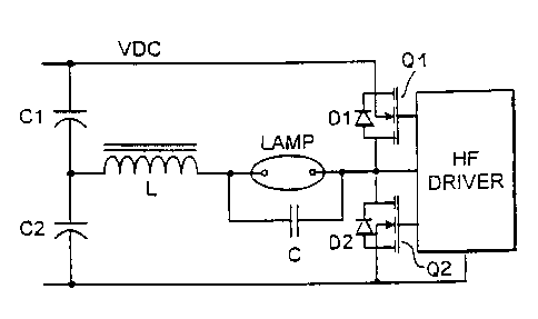
Figure 9 shows the proposed invention circuit.
Figure 10 shows the control signals for Q1 and Q2
in the Fig. 9 circuit.
Figure 11 shows the lamp's operating waveforms as
driven by the Fig. 9 circuit.
Figure 12 shows another proposed invention
circuit.
Figure 13 shows one control method of Q1, Q2, Q3,
and Q4 for the Fig. 12 circuit.
Figure 14 shows the lamp's operating waveforms as
driven by the Fig. 12 circuit with the Fig. 13 control
method.
Figure 15a and Figure 15b shows the second control
method of Ql, Q2, Q3, and Q4 for the Fig. 12 circuit.
Figure 16 shows the lamp's operating waveforms as
driven by the Fig. 12 circuit with the Fig. 15 control
method.
Figure 17 shows a DC-type HID ballast circuit.
Figure 18 shows the driving signal for the Fig. 17
circuit.
Figure 19 shows the lamp's operating waveforms as
driven by the Fig. 17 circuit with the Fig. 18 control
method.
Description of the Preferred Embodiments
Figure 9 shows a half bridge circuit schematic
implementation of the present invention. Figure 12 shows
a full bridge circuit schematic implementation of the
present invention. Which topology to choose is
determined by the power level of the HID ballast. The
operating principles of Fig. 9 and Fig. 12 are almost the
same.
In the Fig. 9 half bridge circuit, L is a buck
inductor and is also a resonant inductor. C is the
resonant capacitor. The switches Q1, Q2 with freewheel
CA 02255512 1998-12-11
_ 7 _
diodes D1 and D2 are power switches. The circuit has two
control loops. One is a current loop; and the other is a
voltage loop. The ballast can work in two operating
modes. One is a low frequency output working mode, and
the other is high frequency lamp starting mode.
In the low frequency output working mode, Q1, D2
and L form a buck chop circuit. The current in the
inductor L is continuous. The output current is
controlled by the current loop. As the power switch Q1
turns on, the DC bulk voltage source (not shown) supplies
energy to the inductor and the lamp. As the power switch
Q1 turns off, D2 turns on to continue the current flow in
the inductor L1, and the inductor L releases its energy
to the lamp. During the DC chopping of Q1 and D2, the
current in the inductor L continues in one direction and
the current on the lamp is a very low ripple DC current.
Because the current in the inductor L has a very low high
frequency ripple, it isn't necessary to use the second
order filter formed by the output inductor L and the
capacitor C parallel with the lamp to filter out the high
frequency ripple current through the lamp to avoid
acoustic resonance. In this case, the value of the
capacitor parallel with the lamp will be determined by
the lamp ignition. It is possible to make the circuit
circulating current as low as possible and still obtain a
voltage magnitude high enough to ignite the lamp. It is
important to note that because the current in the
inductor L is continuous, as the power switch Q1 turns
off, the current of the inductor L passes only through
the diode D2, regardless of whether the power switch Q2
is turned on or off. That is the reason that Q1 and Q2
are still turned on or off alternatively as shown in Fig.
10. In the same way, during the DC chopping of Q2 and
D1, the current in the inductor L continuous in one
direction, opposite to the one in the Q1 and D2 DC
CA 02255512 1998-12-11
_ g _
chopping case. In this way, there is a low frequency
square waveform current to drive the lamp. The current
loop forces the inductor L current to follow the
reference current and control the lamp current. The
frequency and amplitude of the current in the inductor L
are determined by the reference current. The voltage
loop detects the lamp voltage and controls the amplitude
of the reference current. Thus, the lamp power is to
controlled.
In high frequency lamp start mode, Q1 and Q2 turn
on or off alternately. D1 and D2 offer a reactive
current path for the resonant circuit. For a low
circulating current resonant tank, the output impedance
of the tank is high, due to the high value of the
inductor L and the low value of the capacitor C. As the
HID lamp is broken down, the lamp impedance will jump
down to a low value and the circuit's Q will jump down to
a low Q value too. Because the tank output impedance is
too high to drive the lamp, the lamp can't be pushed from
glow to arc and the lamp will extinguish. In order to
decrease the output impedance and to push the lamp from
the glow to the arc, a low frequency source is needed to
add to the tank. Because the high frequency, high
voltage, is generated by the circuit resonance and the Q
of the resonant circuit is high (about 14 to 20), it is
not necessary to keep the duty-cycle around 50%. In the
high frequency lamp starting mode, the duty-cycle DM1 of
Q1 is modulated by the output low frequency square
waveform, that is, PWM control, and similarly for the
duty-cycle DM2 of Q2. DM1 and DM2 have the following
relation.
DMl=1-DM2
CA 02255512 1998-12-11
- 9 -
Because the duty-cycles of Q1 and Q2 have been
modulated, the voltage on the capacitor C parallel with
the lamp is composed of a high frequency high voltage and
a low frequency voltage whose amplitude is determined by
the DC bulk voltage and the equivalent duty-cycle DM1.
It is the low frequency voltage on the capacitor parallel
with the lamp that provides the low frequency energy to
drive the lamp as the lamp is ignited. In this way, the
lamp can start at high frequency then transit to low
frequency automatically. As the lamp current is set up,
the current loop takes over to force the lamp current to
follow the reference current waveform and control the
lamp current. In this way, the ballast can shift from
the high frequency starting mode to the low frequency
working output mode smoothly and there is no delay time
as in the circuit of Figs. 4 and 8.
In the Fig. 12 full bridge circuit, Lr is a buck
inductor and is also a resonant inductor. Cr is the
resonant capacitor. The switches Q1, Q2, Q3, and Q4 with
freewheel diodes D1, D2, D3, D4 are power switches. The
circuit has two control loops. One is a current loop;
and the other is a voltage loop. The ballast also works
in two operating modes. One is a low frequency output
working mode; and the other is a high frequency lamp
starting mode.
In the low frequency output working mode, Q1, D2
and Lr form a buck chop circuit. During the Q1, D2 and
Lr DC chopping period, Q4 is turned on in the whole
period. The current in the inductor Lr is continuous.
The output current is controlled by the current loop. As
the power switch Q1 turns on, the DC bulk voltage source
(not shown) offers energy to the inductor and the lamp.
As the power switch Ql turns off, D2 turns on to continue
the current in the inductor Lr, and the inductor Lr
releases its energy to the lamp. During the DC chopping
CA 02255512 1998-12-11
- 10 -
of Q1 and D2, the current in the inductor Lr continues in
one direction and the current on the lamp is a very low
ripple DC current. Because the current in the inductor
Lr has a very low high frequency ripple, it isn't
necessary to use the second order filter formed by the
output inductor Lr and the capacitor Cr parallel with the
lamp to filter out the high frequency ripple current
through the lamp to avoid acoustic resonance. In this
case, the value of the capacitor Cr parallel with the
lamp will be determined by the lamp ignition. It is
possible to make the resonant tank circulating current as
low as possible and still obtain a voltage magnitude high
enough to ignite the lamp. It is important to note that
because the current in the inductor Lr is continuous, as
the power switch Q1 turns off, the current of the
inductor Lr passes only through the diode D2, regardless
of whether the power switch Q2 is turned on or turned
off. That is the reason that Q2 can turn on or off
alternatively or off as shown in Fig. 13. In the same
way, during the DC chopping of Q3 and D4, Q2 is turned on
during the whole period. The current in the inductor Lr
continues in one direction, opposite to the one in the Ql
and D2 DC chopping case. In this way, because of the DC
chopping of Q1, D2, and Q3, D4, there is a low frequency
square waveform current to drive the lamp. In the
circuit, there is a current loop to force the inductor Lr
current to follow the reference current. The frequency
and amplitude of the current in the inductor Lr are
determined by the frequency and amplitude of the
reference current. It is the current loop that serves as
the lamp current control. In the control circuit, there
is a voltage loop to detect the lamp voltage and control
the amplitude of the reference current. In this way, the
lamp power can be controlled.
CA 02255512 1998-12-11
- 11 -
In high frequency lamp starting mode, there are
two options. Option one is that Q1 and Q4 are turned on
or off with Q2 and Q3 alternately, and D1, D2, D3, D4
offer the reactive current paths for the resonant
circuit. Option two is that Q4 turns on, and Q1 and Q2
turn on or off alternately, and D1 and D2 offer a
reactive current path for the resonant circuit. Which
one should be chosen is determined by the DC bulk voltage
and the circulating current stress.
For option one, Q1 and Q4 are turned on or off
with Q2 and Q3 alternatively shown in Fig. 13. Due to
the high value of the inductor Lr and low value of the
capacitor Cr, the output impedance of the tank is high.
As the HID lamp is broken down, the lamp impedance will
jump down to a low value and the circuit's Q will jump
down to a low Q value too. Because the tank output
impedance is too high to drive the lamp, the lamp can't
be pushed from glow to arc and the lamp will extinguish.
In order to decrease the output impedance and to push the
lamp from the glow to the arc, a low frequency source is
needed to add to the tank. Because the high frequency,
high voltage, is generated by the circuit resonance and
the Q of the resonant circuit is high (about 14 to 20),
in the high frequency lamp starting mode, the duty-cycle
DM1 of Q1 and Q4 is modulated by the output low frequency
square waveform, that is, PWM control, and so similarly
for the duty-cycle DM2 of Q2 and Q3. DM1 and DM2 have
the following relation.
DM1=1-DM2
Because the duty-cycles of Q1 and Q4 and Q2 and Q3
have been modulated, the voltage on the capacitor Cr
parallel with the lamp is composed of a high frequency
high voltage and a low frequency voltage whose amplitude
CA 02255512 1998-12-11
- 12 -
is determined by the DC bulk voltage and the equivalent
duty-cycle DM1. It is the low frequency voltage on the
capacitor parallel with the lamp that supplies the low
frequency energy to drive the lamp as the lamp is
ignited. In this way, the lamp can start at high
frequency then shift to low frequency automatically. As
the lamp current is set up, the current loop serves to
force the lamp current to follow the reference current
waveform and control the lamp current. In this way, the
ballast can shift from the high frequency starting mode
to the low frequency working output mode smoothly and
there is no delay time.
For option two, because Q4 turns on, and Q1 and Q2
turn on or off alternately as shown in Fig. 15(a), the
voltage on the resonant capacitor Cr is composed of a
high frequency, high voltage plus a DC voltage offset
(Fig. 16) whose amplitude is determined by the DC bulk
voltage and the duty-cycle of Q1. It is the high
frequency, high voltage that breaks down the lamp. It is
the DC voltage on Cr that pushes the lamp from the glow
to the arc, as the lamp is broken down. As the lamp
current is set up, the current loop serves to force the
lamp current to follow the current reference. In this
way, the ballast can shift from starting mode to normal
mode automatically and there is no delay time as in the
prior art.
The described technique can also apply to a DC
type HID lamp ballast. The power circuit is shown in
Fig. 17, and the control PWM signals are shown in Fig.
18. In the DC HID ballast, there are a current loop and
voltage loop to control the lamp current and the ballast
output power. For starting mode, switches Q1 and Q2 are
turned on or off alternately shown in Fig. 18(a). The
buck inductor Lr will resonant with the capacitor
parallel with the lamp to produce a high-frequency high
CA 02255512 1998-12-11
- 13 -
voltage plus a DC voltage to break down the lamp. As the
lamp is broken down, the DC voltage will push the lamp
from glow to arc, and as the lamp current is set up, the
lamp current will be forced to follow with the reference
current. The voltage loop is used to control the
reference current to control the input lamp power.