Note : Les descriptions sont présentées dans la langue officielle dans laquelle elles ont été soumises.
CA 022~6378 1998-11-30
W O 98/45881 PCT/JP98/01361
D E S C R I P T I O N
SUBSTRATE WITH CONDUCTOR FORMED OF
S LOW-RESISTANCE ALUMINUM ALLOY
Technical Field
This invention relates to a substrate which has
wiring electrically connected to a semlconductor
element and showing excellent characteristics, and in
particular to a substrate with wiring which has an
excellent anti-hillock characteristic, an excellent
anti-pinhole characteristic and a low resistance, and
is suitable for use in, for example, an active matrix
type liquid crystal display device.
Background Art
There is an active matrix type liquid crystal
display device which has, for example, wiring including
a scanning line 1 and a data line 2, etc., a pixel
electrode 3, and a thin film transistor 4 as a
switching element located in the vicinity of each
intersection of the scanning line 1 and the data line 2,
as is shown in FIG. 10. The thin film transistor 4 has
a gate electrode G connected to the scanning line 1, a
drain electrode D connected to the data line 2, and a
source electrode S connected to the pixel electrode 3.
FIG. 11 shows a cross section of part of the thin
film transistor 4 of FIG. 10. The scanning line 1
including the gate electrode G (see FIG. 10) is formed
CA 022~6378 1998-11-30
W O 98/45881 PCT/JP98/01361
on a predetermined portion of a glass substrate 11, an
anode oxide film 12 is formed on the surface of the
scanning line 1, and a gate insulating film 13 is
formed on the overall surfaces of the lines and the
substrate. A semiconductor thin film 14 made of
amorphous silicon is formed on that portion of the gate
insulating film 13 which corresponds to the gate
electrode G. A blocking layer 15 is formed on a center
portion of the semiconductor thin film 14. Ohmic
contact layers 16 and 17 made of n+-conductivity
silicon are formed on upper opposite side portions of
the semiconductor thin film 14 and the blocking
layer 15. The drain electrode D and the source
electrode S are formed on the ohmic contact layers 16
and 17, respectively. These electrodes D and S and the
data line 2 may be formed simultaneously. The pixel
electrode 3 is formed on a predetermined upper portion
of the gate insulating film 13 such that it is
connected to the source electrode S. A passivation
film 18 is formed on the overall upper surface of the
resultant structure, except for on the surface of the
predetermined portion of the pixel electrode 3.
It is known that an Al (Aluminum) alloy which
contains a high-melting-point metal such as Ti
(Titanium) is used as the material of the wiring
forming the scanning line 1 with the gate electrode G
(see, for example, Jpn. Pat. Appln. KOKAI Publication
CA 022~6378 1998-11-30
W O 98/45881 PCT/JP98/01361
No. 4-130776). In this case, the high-melting-point
metal Ti is contained in Al in order to suppress the
occurrence of hillocks, which may well be formed during
a heating treatment performed later since A~ itself
does not have a sufficient thermal resistance. The
anti-hillock characteristic is considered to, for
example, reduce the breakdown voltage of the gate
insulating film 13 on the scanning line 1 including the
gate electrode G. If the Ti concentration of the Al-Ti
alloy thin film is reduced to lower its specific
resistance, occurrence of any hillock and pinhole
cannot be suppressed. If, on the other hand, the
concentration of Ti is increased, the above drawback
can be countered but the specific resistance of the
alloy thin film increases. This alloy thin film is not
preferable as an electrode or wiring.
Disclosure of Invention
It is the object of the invention to provide a
wiring substrate with a conductor which can reduce the
specific resistance of the substrate to a value equal
to or less than the case of using the Al-Ti alloy thin
film, and also can suppress the occurrence of hillocks
or pinholes.
The inventors of the present invention made
various experiments to test the Al-Ti alloy thin film
in detail. The experiment's results and our opinion
thereon will now be described.
CA 022~6378 1998-11-30
W O 98/45881 PCT/JP98/01361
First, the dependency of the specific resistance
of the Al-Ti alloy thin film upon the concentration of
Ti was tested, and test results as shown in FIG. 5 were
obtained. In FIG. S, the ordinate indicates the
specific resistance of the alloy thin film, the
abscissa the concentration (atomic %) of Ti, the solid
line the specific resistance of an Al-Ti alloy thin
film formed, by sputtering or deposition, on a glass
substrate which is kept at a room temperature, and the
broken line, the one-dot chain line and the two-dot
chain line the specific resistances of Al-Ti alloy thin
films after heating of the Al-Ti alloy thin film formed
at the room temperature, at temperatures of 2S0~C, 300~C
and 350~C, respectively. As is evident from FIG. 5, in
all the Al-Ti alloy thin films, the higher the
concentration of Ti, the higher the specific resistance.
Further, the higher the heat treatment temperature, the
lower the specific resistance. Thus, it was confirmed
from the experiments that the lower the Ti
concentration, the lower the specific resistance of the
Al-Ti alloy thin film, and that the higher the heat
treatment temperature, the lower the specific
resistance.
Moreover, the anti-hillock characteristic of each
of the Al-Ti alloy thin films was tested, and test
results as shown in FIG. 6 were obtained. In FIG. 6,
the ordinate indicates the temperature at which a
_ .
CA 022~6378 1998-11-30
W O 98/45881 PCT/JP98/01361
hillock or hillocks occur. More specifically, the
hillock occurrence temperature means a heat treatment
temperature at which any hillock with a height of 0.5 -
1 ~ m or more can be observed using an-electron
S microscope with a magnification of about 100
(hereinafter, the hillock occurrence temperature means
the same). As is evident from FIG. 6, the occurrence
of a hillock can be suppressed if the heat treatment
temperature is 250~C and the Ti concentration is 3 atm%
or more. In light of the anti-hillock characteristic,
it is desirable to set the Ti concentration at 3 atm%
or more through the overall process of forming the
wiring substrate, when a heat treatment is performed at
about 250~C at highest in the process. In the case of a
heat treatment temperature of 250~C indicated by the
broken line in FIG. 5, however, the specific resistance
is about 18 ~Q cm or more if the Ti concentration is
3 atm% or more. In other words, when the anti-hillock
characteristic is considered, it is not preferable to
set the Ti concentration at 3 atm% or less, which means
that the specific resistance of the wiring (the
scanning line 1 including the gate electrode G) cannot
be set at about 18 ~Q cm or less. On the other hand,
more and more reduction of the resistance of wiring has
recently been requested with the development of
refining techniques, the increase of the numerical
aperture, etc. in the field of liquid crystal display
CA 022~6378 1998-11-30
W O 98/45881 PCT/JP98/01361
devices. To meet the request, attention has been paid
to an Al alloy containing a rare earth metal such as Nd,
which has an excellent anti-hillock characteristic and
a low specific resistance of about 10 ~ Q cm or less
(see, for example, Jpn. Pat. Appln. KOKAI Publication
No. 7-45555).
However, the inventors of the present invention
made experiments using an Al-Nd alloy thin film, and
obtained the following results. First, the dependency
of the specific resistance of the Al-Nd alloy thin film
upon the Nd (Neodymium) concentration was tested, and
test results as shown in FIG. 7 were obtained. In
FIG. 7, the ordinate indicates the specific resistance
of the alloy thin film, and the abscissa the Nd
concentration. Further, the solid line indicates the
specific resistance, with respect to the Nd
concentration, of an Al-Nd alloy thin film formed, by
sputtering or deposition, on a glass substrate which is
kept at a room temperature, and the broken line, the
one-dot chain line and the two-dot chain line the
specific resistances of Al-Nd alloy thin films after
heating of the Al-Nd alloy thin film formed at the room
temperature, at temperatures of 250~C, 300'C and 350~C,
respectively. As is evident from FIG. 7, in all the
Al-Nd alloy thin films, the higher the concentration of
Nd, the higher the specific resistance. Further, when
the Nd concentration is, for example, 2 - 4 atm~, the
CA 022~6378 1998-ll-30
W O 98/45881 PCT/JP98/01361
specific resistances of all the heated Al-Nd alloy thin
films are about 10 ~Q cm or less. Thus, it was
confirmed that the specific resistances of the Al-Nd
alloy thin films can be set at 10 ~Q cm or less.
Moreover, the anti-hillock characteristic of each
of the Al-Nd alloy thin film was tested, and test
results as shown in FIG. 8 were obtained. In FIG. 8,
the abscissa indicates the Nd concentration, and the
ordinate the temperature at which a hillock or hillocks
occur. As is evident from FIG. 8, the occurrence of a
hillock can be suppressed when the heat treatment
highest temperature is 250~C, even if the Nd
concentration is as low as about 0.2 %. It was
confirmed that when the Nd concentration is, for
lS example, about 2 - 4 atm%, the occurrence of a hillock
is suppressed, and that the specific resistance is
about 10 ~Q cm or less, as indicated by the broken
line (the heat treatment temperature of 250'~).
Moreover, the anti-pinhole characteristic of each
of the Al-Nd alloy thin film was tested, and test
results as shown in FIG. 9 were obtained. In FIG. 9,
the ordinate indicates the temperature at which a
pinhole or pinholes occur. More specifically, the
pinhole occurrence temperature means a heat treatment
temperature at which more than ten pinholes can be
observed per 1 cm2 using an electron microscope with a
magnification of about 100 (hereinafter, the pinhole
CA 022~6378 1998-11-30
W O 98/45881 PCT/JP98/01361
occurrence temperature means the same). As is evident
from FIG. 9, the pinhole occurrence temperature is less
than 250'C if the Nd concentration is about 4 atm% or
less, and is substantially 250~-C if the Nd concentration
is about 4 atm% or more. In light of the anti-pinhole
characteristic, it is desirable to set the Nd concen-
tration at about 4 atm% or more when the heat treatment
temperature is 250~C. It was found, however, that more
and more increase of the Nd concentration will not be
so effective to enhance the anti-pinhole characteristic
for protecting wiring from breakage, since the pinhole
occurrence temperature is substantially kept at about
250C when the Nd concentration is about 4 atm% or more.
Furthermore, where the Nd concentration is set at
4 atm% or more in consideration of the anti-pinhole
characteristic, the specific resistance is about
10 ~Q cm or more at the heat treatment temperature of
250GC indicated by the broken line in FIG. 7.
As described above, in the case of using the Al-Ti
alloy thin film as wiring, it is not preferable to set
the Ti concentration at 3 atm% or less in light of the
anti-hillock characteristic, which makes it impossible
to set the specific resistance at about 18 ~Q cm or
less. On the other hand, in the case of using the Al-
Nd alloy thin film as wiring, setting the Ndconcentration at 4 atm% or more cannot significantly
enhance the anti-pinhole characteristic for protecting
CA 022~6378 1998-11-30
WO98/45881 PCT/~98/01361
the wiring from breakage. In addition, setting the Nd
concentration at 4 atm% or more in consideration of the
anti-pinhole characteristic makes the specific
resistance increase to about lO ~Q cm or more as
indicated by the ~roken line in FIG. 7 (the heat
treatment temperature of 250~C~.
The present invention, which has been devised in
view of the above problems, provides a wiring substrate
comprising a substrate and a conductor formed on the
substrate, the conductor formed of an aluminum alloy
which contains at least neodymiu~ and titanium.
Brief Description of Drawings
FIG. l is an enlarged sectional view, showing a
substrate with wiring formed of an Al-Nd-Ti alloy thin
lS film, according to an embodiment of the invention;
FIG. 2 is a view, showing the dependency of the
specific resistance of the Al-Nd-Ti alloy thin film of
FIG. l upon the concentration of Ti;
FIG. 3 is a view, showing the dependency of the
anti-hillock characteristic of the Al-Nd-Ti alloy thin
film of FIG. l upon the concentrations of Ti and Nd;
FIG. 4 is a view, showing the dependency of the
anti-pinhole characteristic of the Al-Nd-Ti alloy thin
film of FIG. l upon the concentrations of Ti and Nd;
FIG. 5 is a view, showing the dependency of the
specific resistance of an Al-Ti alloy thin film upon
the concentration of Ti;
. ., ~ .. ..
CA 022~6378 1998-11-30
WO98/45881 PCT/~98/01361
FIG. 6 is a view, showing the anti-hillock
characteristic of the Al-Ti alloy thin film;
FIG. 7 is a view, showing the dependency of the
specific resistance of an Al-Nd alloy thin film upon
the concentration of Nd;
FIG. 8 is a view, showing the anti-hillock
characteristic of the Al-Nd alloy thin film;
FIG. 9 is a view, showing the anti-pinhole
characteristic of the Al-Nd alloy thin film;
FIG. lO is a circuit diagram, showing part of the
conventional liquid crystal display device; and
FIG. ll is an enlarged sectional view, showing, in
detail, a thin film transistor which appears in FIG. lO.
Best Mode of Carrying Out the Invention
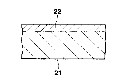
FIG. l an enlarged sectional view, showing a
wiring substrate according to the embodiment of the
invention. An Al-Nd-Ti alloy thin film (wiring) 22 was
formed on a glass substrate (transparent insulated
substrate) 21 by sputtering or deposition. The
wiring 22 is used as the scanning line l or the data
line 2 shown in FIG. lO. First, the dependency, upon
the concentrations of Ti and Nd, of the specific
resistance of an Al-Nd-Ti alloy thin film formed by
setting the substrate temperature at a room temperature
was tested, and test results as shown in FIG. 2 were
obtained. In the test, the minimum concentrations of
Nd and Ti were O.l atm%. In FIG. 2, the specific
CA 022~6378 1998-11-30
W O 98/45881 PCT/JP98/01361
resistance is 10 ~Q cm or less in an area A1, 10 -
20 ~Q cm in an area A2, 20 - 30 ~Q cm in an area A3,
30 - 40 ~Q cm in an area A4, 40 - 50 ~Q cm in an area
As, 50 - 60 ~Q cm in an area A6, and 60 - 70 /lQ cm in
an area A7. As is evident from FIG. 2, the higher the
Nd and Ti concentrations, the higher the specific
resistance. Further, FIG. 2 shows that the Nd and Ti
concentrations should be selected from the area Al in
order to set, at about 10 ~Q cm or less, the specific
resistance of the Al-Nd-Ti alloy thin film formed with
the substrate temperature kept at a room temperature.
Similarly, the Nd and Ti concentrations should be
selected from the areas Al and A2 in order to set the
specific resistance at about 20 ~Q cm or less.
Then, the dependency of the hillock characteristic
of the Al-Nd-Ti alloy thin film upon the concentrations
of Ti and Nd was tested, and test results as shown in
FIG. 3 were obtained. In FIG. 3, the hillock
occurrence temperature is 240 - 270~C in an area Bl,
270 - 300-C in an area B2, 300 - 330C in an area B3, and
330 - 360~C in an area B4. As is evident from FIG. 3,
the occurrence of a hillock is suppressed in the area
Bl when the heat treatment temperature is 240 - 270~C.
Further, the dependency of the pinhole
characteristic of the Al-Nd-Ti alloy thin film upon the
concentrations of Ti and Nd was tested, and test
results as shown in FIG. 4 were obtained. In FIG. 4,
CA 022~6378 1998-11-30
W O 98/45881 PCT/JP98/01361
the pinhole occurrence temperature is 240 - 270~C in an
area Cl, 270 - 300~C in an area C2, 300 - 330~C in an
area C3, and 330 - 360~C in an area C4. As is evident
from FIG. 4, the occurrence of a pinhole is suppressed
in the area Cl when the heat treatment temperature is
240 - 270~C.
In a case, for example, where the Nd concentration
is 0.75 atm% and the Ti concentration is 0.5 atm%, the
hillock occurrence temperature is on the boundary
between the areas Bl and B2 in FIG. 3, while the
pinhole occurrence temperature is on the boundary
between the areas Cl and C2 in FIG. 4. Accordingly,
the occurrence of any hillock and any pinhole can be
suppressed by setting the heat treatment temperature at
240 - 270~C. Moreover, when the Nd and Ti
concentrations are 0.75 atm% and 0.5 atm%, respectively,
the specific resistance falls in the area Al (10 u Q cm
or less) in FIG. 2, and the specific resistance of the
Al-Nd-Ti alloy thin film formed by setting the
substrate temperature at a room temperature can be set
at about 8 ~ Q cm. In addition, it is roughly
estimated from FIGS. 5 and 7 that the specific
resistance can be made lower than about 8 ~ Q cm by the
heat treatment. In other words, when the heat
treatment is performed, the area A1 in which the
specific resistance can be kept at 10 ~ Q cm or less is
}:)roadened to the area A2 in FIG. 2. Accordingly, the
CA 022~6378 1998-11-30
W O 98f45881 PCT/JP98/01361
- specific resistance of the Al-Nd-Ti alloy thin film
after the heat treatment is set at about 10 ~Q cm or
less by setting the total of the Nd and Ti
concentrations to about 1.5 atm% or less (each of the
Nd concentration and the Ti concentration should be set
at 0.1 atm% or more). Furthermore, as is evident from
FIGS. 3 and 4, the occurrence of a hillock and a
pinhole can be substantially suppressed in the case of
the total concentration range of about 1.5 atm% or less,
when the heat treatment is 240 - 270~C.
A description will be given of a case where the
specific resistance of the Al-Nd-Ti alloy thin film is
set at about 18 ~Q cm as in the Al-Ti alloy thin film.
If the total of the Nd and Ti concentrations to, for
example, about 3.5 atm% or less (each of the Nd
concentration and the Ti concentration should be set at
0.1 atm% or more), the specific resistance of the Al-
Nd-Ti alloy thin film formed by setting the substrate
temperature at the room temperature is about 20 ~ Q cm
or less as shown in FIG. 2. In the case of the total
concentration range of about 3.5 atm% or less, it is
evident from FIGS. 3 and 4 that although a small number
of hillocks or pinholes occur when the heat treatment
temperature is 240 - 270~C, their occurrence can be
suppressed by increasing the heat treatment temperature.
Also in this case, it is roughly estimated from FIGS. 5
and 7 that the specific resistance can be made lower
CA 022~6378 1998-ll-30
W O 98/45881 PCT/JP98/01361
than about 20 ~Q cm by the heat treatment. In other
words, when the heat treatment is performed, the
specific resistance of the Al-Nd-Ti alloy thin film can
be set to about 18 ~Q cm or less.
The Nd concentration of the Al-Nd-Ti alloy thin
film will be considered. In the area C1 in FIG. 4, for
example, a pinhole will occur irrespective of the Nd
concentration when the heat treatment temperature is
240 - 270''C. On the other hand, in the area Bl in
FIG. 3, a hillock will occur at the heat treatment
temperature of 240 - 270~C, if the Nd concentration is
lower than 1 atm%. This means that the Nd
concentration may be set at about 1 atm% by considering
the occurrence of a hillock and not the occurrence of a
pinhole. When the Nd concentration is set at about
1 atm%, it is preferable, in light of the specific
resistance, to set the Ti concentration at about
0.1 - 2 atm%, and more preferable to set it at about
0.1 - 0.5 atm%.
In the case of the Al-Ti alloy thin film, it is
preferable to set the Ti concentration at about
2.9 atm% to realize a lower specific resistance and an
excellent anti-hillock characteristic (at the heat
treatment temperature of 250C), as is shown in FIGS. 5
and 6. In the case of the Al-Nd alloy thin film, it is
preferable to set the Nd concentration at about 4 atm%
to realize a lower specific resistance and an excellent
CA 022~6378 1998-11-30
W O 98/45881 PCT/JP98/01361
anti-hillock characteristic (at the heat treatment
temperature of 250~C), as is shown in FIGS. 7 and 9. On
the other hand, in the case of the Al-Nd-Ti alloy thin
film, the total concentration of Nd and Ti can be set
at about 1.5 atm% or less. Therefore, when the Al-Nd-
Ti alloy thin film is used, the required amounts of
expensive Nd and Ti can be reduced as compared with the
case of the Al alloy thin film which contains only Ti
or Nd. This will lead to reduction of a manufacturing
cost.
Although in the above description, the substrate
of the invention is applied to a display device, it can
also be applied to various devices other than the
display device. Further, the wiring is not limited to
the scanning line which includes the gate electrode of
the thin film transistor, but may be used as a source
electrode, a drain electrode or a data line. This case
will be briefly explained with reference to FIG. 11.
To provide, for example, a data line of an Al-Nd-Ti
alloy thin film on a gate insulating film 4 by
patterning, an n+-type silicon layer or a chromium
layer may be formed on the gate insulating film 4 to
prevent a pixel electrode 11 made of ITO from being
damaged by an Al etching solution, and then an Al-Nd-Ti
alloy thin film may be formed on the resultant
structure for forming, for example, a data line.
Moreover, the wiring is not limited to the Al-Nd-Ti
..~.. ~ ~
CA 022~6378 1998-ll-30
W O 98/45881 PCT/JP98/01361
16
alloy thin film, but may be formed of an Al alloy thin
film which contains one or more rare earth elements and
one or more Ti, Ta, Mo, Cr, Au, Ag, Cu.
As described above, according to the invention, to
form wiring of, for example, an Al-Nd-Ti alloy thin
film enables reduction of its specific resistance to a
value equal to or lower than the wiring formed of the
Al-Ti alloy thin film, and also enables suppression of
the occurrence of a hillock or a pinhole. In this case,
it is preferable to set the total concentration of Nd
and Ti at from about 3.5 atm% or less to about 0.2 atm%
or more (supposing that the Nd concentration is equal
to the Ti concentration). Also, it is preferable to
set the specific resistance of the Al-Nd-Ti alloy thin
film at about lO - l ~ Q cm.