Note : Les descriptions sont présentées dans la langue officielle dans laquelle elles ont été soumises.
CA 022~7887 1998-12-lo
W O 98/00912 - PCTAUS97/06165
BIAS CIRCUIT FOR A POWER AMPLIFIER
Field of the Invention
This invention relates to linear power amplifiers, including
10 but not limited to biasing of Doherty-type amplifiers.
Background of the Invention
15 It is desirable for radio frequency (RF) power amplifiers to
linearly amplify RF signals in a highly efficient manner.
Nevertheless, there are tradeoffs between maximum efficiency
and high linearity. Efficiency is generally proportional to input
drive level, and high efficiency is usually not att~ined until an
20 amplifier approaches its m~ximum output power, which is not
consistent with linear operation. Doherty-type amplifiers
achieve an efficiency advantage over standard class AB and
class B amplifiers below peak power, in part, because of an
instantaneous modulation of their carrier amplifier's loadline
25 as the RF input level changes. In other words, Doherty-type
amplifiers exhibit a more benign relationship between input
drive level and efficiency because the amplifier's loadline is
continuously modified to maintain high efficiency as input
drive level changes. In addition, the bias power of Doherty-
30 type amplifiers is greatly reduced over standard class AB and
~ class B amplifiers.
A method of biasing a Doherty-type amplifier is described
in U.S. Patent Application No. 08/566,811, titled "LINEAR
3 5 POWER AMPLIFIER USING ACTIVE BIAS FOR HIGH EFFICIENCY ~ND
CA 022~7887 1998-12-10
W O 98/00912 - rCT~US97/06165
METHOD THEREFOR," filed on December 4, 1995 on behalf of
BERNARD E. SIGMON et al., with the same assignee as the
present invention, which application is incorporated herein by
reference. The circuit described in the above-referenced
5 application relies on changes in the gate or base bias current
of the carrier amplifier as a way to measure RF input power to
that device. Such a me~h~nism is not effective for MOSFET
(metal oxide semiconductor field effect transistor) amplifier
devices, because such devices do not draw bias current at any
10 RF drive level.
Accordingly, there is a need for a bias circuit for a Doherty-
type amplifier that provides good biasing for MOSFET or other
zero bias current amplifiers, but is efficient over the the
15 dynamic RF input drive range.
Brief Description of the Drawings
20 FIG. 1 is a block diagram of a Doherty-type power amplifier
with bias control in accordance with the invention.
FIG. 2 is a block diagram of an alternate use of a Doherty-
type power amplifier with bias control in accordance with the
invention.
25 FIG. 3 is a block diagram of a bias control circuit for a
carrier amplifier in accordance with the invention.
FIG. 4 is a block diagram of a bias control circuit for a
peaking amplifier in accordance with the invention.
FIG. 5A and FIG. 5B are graphical representations of bias
30 control signals in accordance with the invention.
FIG. 6 is a block diagram of a carrier amplifier or a peaking
amplifier in accordance with the invention.
CA 022~7887 1998-12-10
W O 98/00912 - PCTrUS97106165
Description of a Preferred Embodiment
The following describes an apparatus for and method of
5 bias control for a Doherty-type power amplifier. The Doherty
power amplifier is comprised of a carrier amplifier and a
peaking amplifier. Different bias signals are provided to the
carrier amplifier and the peaking amplifier to provide constant
power gain while limiting intermodulation distortion. In one
10 embodiment, the carrier amplifier bias signal decreases as the
peaking amplifier bias signal increases.
The present invention provides a power amplifier
comprising a power divider coupled to an RF input signal for
15 producing an in-phase signal and a quadrature phase signal
from the RF input signal. A carrier amplifier amplifies the in-
phase signal from the power divider and has a carrier
amplifier bias input. A peaking amplifier amplifies the
quadrature phase signal from the power divider and has a
20 peaking amplifier bias input. A combiner is coupled to an
output of the carrier amplifier and an output of the peaking
amplifier. The combiner combines in additive phase the
output of the carrier amplifier and the output of the peaking
amplifier. A first bias circuit is coupled to the carrier
25 amplifier, wherein the carrier amplifier bias input is provided
by the first bias circuit and controlled by a first signal
indicative of the m~gnitude of the RF input signal of the power
amplifier. A second bias circuit is coupled to the peaking
amplifier, wherein the peaking amplifier bias input is provided
30 by the second bias circuit and controlled by a second signal
indicative of the m~gnitude of the RF input signal of the power
amplifier. Alternatively, the first signal and the second signal
may be the same signal. In addition, the first signal and/or the
second signal may be derived from an output of an envelope
35 detector that is coupled to the RF input signal. Furthermore,
CA 022~7887 1998-12-lo
W O 98/00912 - PCT~US97/06165
the first signal and/or the second signal may be proportional
to a current drawn by the carrier amplifier. Additionally, the
carrier amplifier bias level may be decreased as the peaking
amplifier bias level is increased.
A method for amplifying an RF input signal using a power
amplifier comprises the steps of dividing the RF input signal
into an in-phase signal and a quadrature phase signal. A
carrier amplifier bias input signal is varied relative to the
10 m~gnitude of the RF input signal. A peaking amplifier bias
input signal is varied relative to the m~gnitude of the RF input
signal. The in-phase signal is amplified using a carrier
amplifier to produce a first amplified signal. The quadrature
phase signal is amplified using a peaking amplifier to produce
15 a second amplified signal. The first amplified signal and the
second amplified signal are combined, in phase, to produce an
output signal. Alternatively, the step of varying the carrier
amplifier bias input signal and the step of varying the peaking
amplifier bias input signal may be performed such that the
20 carrier amplifier bias input signal decreases as the peaking
amplifier bias input signal increases. Envelope detecting the RF
input signal may be performed to derive the m~gnitude of the
RF input signal. The m~gnitude of the RF input signal may be
determined from a current drawn by the carrier amplifier.
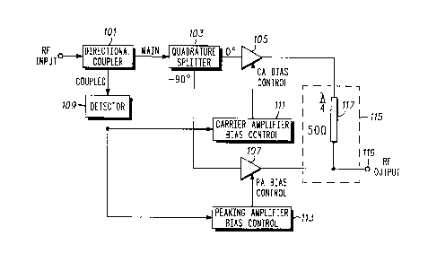
A block diagram of a Doherty-type power amplifier with
bias control is shown in FIG. 1. An RF input signal is fed into a
directional coupler 101 that performs the function of
providing a small sample of the input signal at its coupled
30 output while delivering the maiority of the input signal power
to the main output. The main output of the directional
coupler 101 is input to a quadrature splitter 103. Due to
splitting, the in-phase signal and the quadrature phase signal
are 3 dB less in m~gnitude than RF input signal. The in-phase
35 (0~) output of the quadrature splitter 103 is input to a carrier
CA 022~7887 1998-12-10
WO 98/00912 - PCT/US97/06165
amplifier 105. The quadrature phase (minus 90~) output of
the quadrature splitter 103 is input to a peaking amplifier 107.
The coupled output of the directional coupler 101 is input to a
detector 109. The detector may be a diode envelope detector
5 such as described in Chapter 9 of the book Solid State Radio
Engineering by Herbert L. Krauss et al., (John Wiley & Sons,
New York, 1980).
The output of the detector 109 is an indication of the RF
10 input power level of the RF input signal, as well as the
m~gnitude of the RF input signal. The detector 109 may be set
up to indicate either peak or average power. The output of
the detector is input to a carrier amplifier bias control 111
and a peaking amplifier bias control 113. The output of the
15 carrier amplifier bias control 111 is a CA bias control signal,
which is input to the bias control input of the carrier amplifier
105. In the preferred embodiment, the carrier amplifier is
biased slightly above cutoff when the detector 109 output
indicates a low input signal level. This process allows the
20 carrier amplifier to provide linear amplification at low input
signal levels. The output of the peaking amplifier bias control
113 is a PA bias control signal, which is input to the bias
control input signal of the peaking amplifier 107. In the
preferred embodiment, the peaking amplifier is biased belo~
25 cutoff when the detector 109 output indicates a low input
signal level. This process improves efficiency at low input
signal levels by preventing the peaking amplifier from drawing
current until the RF input signal has reached about half of its
maximum permitted amplitude.
The output of the carrier amplifier 10~ and the output of
the peaking amplifier 107 are input to a combiner 115. In the
preferred embodiment, the combiner is composed of a quarter
wave length (l/4) 50 ohm transmission line 117, the output of
35 which is connected to the peaking amplifier output at the RF
CA 022~7887 1998-12-10
W O 98/00912 - PCT~US97/06165
output port 119. At low input signal levels, the peaking
amplifier is inactive and presents a high impedance to the
combiner 115 at the RF output port 119. In the preferred
embodiment, the impedance at the RF output port is nomin~lly
5 25 ohms, and the (l/4) S0 ohm transmission line 117,
transforms this impedance to 100 ohms at the output of the
carrier amplifier. Because the carrier amplifier is designed to
operate into a nominal 50 ohm load, presenting a 100 ohm
load causes the carrier amplifier to saturate at half its nominal
10 maximum output power level when the RF input signal reaches
half of its maximum permitted amplitude. At this point, the
amplitude of the RF input signal causes the peaking amplifier
to start delivering power to the RF output port 119. Under
these conditions, the (l/4) 50 ohm transmission line 117 also
15 insures that the outputs of both the carrier and peaking
amplifiers add in phase at the RF output port 119, so as to
provide the maximum available output power and efficiency.
A filter may also be inserted between the detector 109 and the
bias control circuits 111 and 113 in order to remove any AC
20 component or short term envelope fluctuations from the
detector 109 output that may degrade intermodulation
distortion.
If the carrier amplifier 105 and peaking amplifier 107
25 operated in the ideal manner described above, the bias levels
could remain fixed at the levels established at zero detector
output, i.e., there would be no need for any bias control
circuitry. This situation is seldom, however, true in practice.
For example, the peaking amplifier 107 may have inadequate
30 gain if it is biased so as to remain inactive until the RF input
signal reaches half of its maximum permitted amplitude. In
this case, it is advantageous to increase the bias on the
peaking amplifier 107 when the RF input signal exceeds half of
its maximum permitted amplitude. In addition, it may be
35 advantageous to reduce the bias on the carrier amplifier 105
CA 022~7887 1998-12-1o
W O98/00912 - PCTrUS97/06165
at some other RF input signal level, in order to maintain a
constant gain in the Doherty-type power amplifier over a wide
range of input signal levels. This process improves the
linearity of the Doherty-type power amplifier, thus reducing
5 the level of intermodulation distortion at the RF output port
119.
The detector 109 may be connected elsewhere in the
circuit, so as to monitor a different operating condition, such
10 as the carrier amplifier 105 and/or peaking amplifier 107 RF
output(s) or DC input current(s). The final choice of detector
109 location and function may be made to optimize the
overall characteristics of the Doherty amplifier (e.g.,
efficiency, gain, gain flatness, intermodulation distortion, and
15 so forth). An alternative embodiment is shown in FIG. 2.
An alternate embodiment of a Doherty-type power
amplifier with bias control is shown in FIG. 2. An RF input
signal is fed into a quadrature splitter 203. The in-phase (0~)
output of the quadrature splitter 203is input to a carrier
amplifier 205. The quadrature phase (minus 90~) output of
the quadrature splitter 203is input to a peaking amplifier 207.
A differential amplifier 209is placed across a resistor Rs,
which is in series with the D( power input to the carrier
25 amplifier 205. The voltage across this resistor is proportional
to the DC current drawn by the carrier amplifier 205, which
current is, in turn, proportional to the RF input power level of
the RF input signal. The output of the differential amplifier
209 is an amplified replica of the voltage across resistor Rs.
The output of the carrier amplifier bias control circuit 211 is
input to the carrier amplifier 205 bias control. The output of
the peaking amplifier bias control circuit 213 is input to the
peaking amplifier 207 bias control input. The output of the
carrier amplifier 205 and the peaking amplifier are combined
35 in combiner 215, which includes a quarter wave length (l/4)
CA 022~7887 1998-12-lo
W O 98/00912 - PCTAUS97/06165
50 ohm transmission line 217, yielding an output at node 219,
similar to the function of the combiner 115 as described with
respect to FIG. 1.
5 A block diagram of a bias control circuit for a carrier
amplifier is shown in FIG. 3. The carrier amplifier bias control
circuit 111 or 211 outputs a CA bias control signal that is
input to the carrier amplifier 105 or 205. An operational
amplifier 301 with its power supply input coupled to Vcc has
10 its positive input coupled to reference voltage Vos. Vos is the
offset voltage reference. The negative input of the operational
amplifier 301 has a resistor R1 in series with the input to the
bias control circuit. In the case of FIG. 1, the bias control
circuit input signal is the detector 109 output signal. In the
15 case of FIG.2, the bias control circuit input signal is the output
of the differential amplifier 209. A resistor R2 is coupled in
series between the negative input of the operational amplifier
301 and the output of the operational amplifier 301.
20 A block diagram of a bias control circuit for a peaking
amplifier is shown in FIG. 4. The peaking amplifier bias
control circuit 113 or 213 outputs a PA bias control signal that
is input to the peaking amplifier 107 or 207. An operational
amplifier 401 with its power supply input coupled to Vcc has
25 its positive input coupled to the input signal to the bias
control circuit 113 or 213. In the case of FIG. 1, the bias
control circuit input signal is the detector 109 output signal.
In the case of FIG. 2, the bias control circuit input signal is the
output of the differential amplifier 209. A series resistor R3 is
30 placed between reference voltage Vos and the negative input
of the differential amplifier. Another series resistor R4 is
coupled in series between the negative input of the operational
amplifier 401 and the output of the operational amplifier 401.
CA 022~7887 1998-12-lo
W O 98/00912 PCTrUS97/06165
The bias control circuits 111, 113, 211, and 213 as shown
are designed to handle a positive voltage as their input signal.
The bias control circuits 111, 113, 211, and 213 may be easily
modified by one of skill in the art to handle negative input
signals.
A graph of the CA bias control signal with respect to the
detector output is shown in FIG. 5A. The CA bias control signal
tracks in the opposite direction as the detector 109 or 209
output. The CA bias control signal remains near Vcc until the
detector 109 or 209 output (Vdet) reaches a level of
substantially Vos ~ (Vos-Vcc)R1/R2. The CA bias control
signal then falls at a slope determined by the ratio -R2/Rl until
it reaches a level near zero.
For example, assume that the CA bias control signal needs
to vary from 5 V to 0 V as the detector 109 or 209 output goes
from 4 V to S V, which is a slope of -5. The first step is to set
Vcc= 5 V in order to get the desired range of variation in the
CA bias control signal. Next, the ratio R2/R1 must be equal to
5 in order to get the desired slope, which is accomplished by
setting R1 = 1000 ohms and R2 = 5000 ohms. Finally, solving
the above equation for Vos with Vdet = 4V and Vcc = 5V gives
the required value of Vos, which is approximately 4.17 V.
It should be noted that the carrier amplifier bias control
circuit of FIG. 3 may also be used for differential amplifier
209. In this caset the reference voltage Vos is connected to
the end of Rs nearest the supply voltage DC and the terminal
labeled INPUT is connected to the opposite end of Rs. The
overall current to voltage transfer function is RSR2/Rl.
A graph of the PA bias control signal with respect to the
detector output is shown in FIG. 5B. The PA bias control signal
tracks in the same direction as the detector 109 or 209
CA 022~7887 1998-12-lo
W O 98/00912 - PCTAUS97/06165
output. The PA bias control signal r~m~ins near zero until the
detector 109 or 209 output (Vdet) reaches a level of
substantially (Vos)R4/(R3+R4). The PA bias control signal then
rises at a slope determined by the ratio (R3+R4)/R3 until it
5 reaches a level near Vcc.
For example, assume that the PA bias control signal needs to
vary from 0 V to 5 V as the detector 109 or 209 output goes
from 2.5 V to 5 V, which is a slope of 2. The first step is to set
10 Vcc = 5 V in order to get the desired range of variation in the
PA bias control signal. Next, the ratio (R3+R4)/R3 must be
equal to 2 in order to get the desired slope, which is
accomplished by setting R3 = 1000 ohms and R4 = 1000 ohms.
Finally, solving the above equation for Vos with Vdet = 2.5 V
15 and Vcc = 5 V gives the required value of Vos, which is 5 V.
A block diagram of a carrier amplifier 105 or 205 or a
peaking amplifier 107 or 207 is shown in FIG. 6. The input to
the amplifier of FIG. 6 is connected to an input matching
20 circuit 601. The output of the input matching circuit is
connected to the gate of a RF power amplifying device 603.
The power amplifying device 603 may be a MOSFET power
amplifying device, for example VMOS or LDMOS. The function
of the input matching circuit 601 is to transform the RF
25 impedance at the gate of the MOSFET device 603, which is
typically around 1 ohm, to the level required for optimum
functioning of the RF input source, which is typically 50 ohms.
The input matching circuit may be constructed by using
various combinations of reactive components, transformers,
30 and transmission lines, as described in the book Solid State
Radio Engineering by Herbert L. Krauss et al., (John Wiley &
Sons, New York, 1980). The gate of the transistor 603 is
connected to voltage supply Vgg through resistor Rs. The gate
of transistor 603 is also connected to ground through resistor
35 R6. The source of transistor 603 is connected to ground. The
CA 022~7887 1998-12-lo
W O 98/00912 - PCT~US97/06165
drain of transistor 603 is connected to supply voltage Vdd via
RF choke 605. The bias control input is connected to the gate
of the transistor 603 via resistor Rgc. Rgc is chosen to give the
desired variation in gate bias voltage Vg as the detector output
5 goes from minimum to maximum. This variation in Vg is
substantially Vcc*1000/(1000+Rgc), assuming that R5 = R6 =
2000 ohms. Vgg is then set, with the appropriate bias control
circuit 111, 113, 211, or 213 connected, to give the desired Vg
at minimum detector 109 or 209 output. The drain of
10 transistor 603 is connected to an output matching circuit 607,
which transforms the impedance at the drain of the MOSFET
device 603, which is typically around 1 ohm, to the impedance
at the RF output port 119, which is typically 50 ohms. The
output matching circuit may be constructed by using various
15 combinations of reactive components, transformers, and
transmission lines, as described in the book Solid State Radio
Engineering by Herbert L. Krauss et al., (John Wiley & Sons,
New York, 1980). The output matching circuit outputs the RF
output of the amplifier.
The present invention provides bias control of Doherty
power amplifiers having zero bias current. The biasing
scheme described above provides improved efficiency
compared to prior art Doherty amplifiers using MOSFET
2 5 devices by keeping the peaking amplifier in hard cutoff until
the carrier amplifier has reached its saturation point. This
biasing scheme also maintains a more constant power gain as a
function of power level in the Doherty power amplifier
because the bias to the carrier amplifier is decreased as the
30 bias to the peaking amplifier is increased. This reduction in
gain variation leads to reduced intermodulation distortion
(improved linearity) in the Doherty power amplifier.
What is claimed is: