Note : Les descriptions sont présentées dans la langue officielle dans laquelle elles ont été soumises.
CA 02260918 1999-01-19
WO98/05141 PCT~S97108568
METHOD AND APPARAT~S FOR RECEIVING A SIGNAL IN
A DIGITAL RADIO FREQ~ENCY COMMUNICATION SYSTEM
Field of the In~Qntion
This invention relates generally to wireless
communication systems, and, more particularly, to a
method and apparatus for receiving a signal in a digital
radio frequency communication system.
Background of the In~ention
In a typical wireless communication system such as
a digital radio frequency (RF) radiotelephone system, a
base station having a controller and a plurality of
transmitters and receivers communicates via an RF
channel with a mobile station operating within an area
served by the base station.
Transmittlng a communication signal over an RF
channel through a medium such as air causes a received
communication signal to significantly differ from the
originally transmitted communication signal. For
example, the transmitted communication signal may be
altered by slowly-changing channel parameters such as
channel gain, phase shift and time delay, and may
further be corrupted by an amount of noise. To produce
an accurate estimate of the originally transmitted
signal, it is important for a receiver, particularly a
non-coherent receiver, to maintain accurate timing
during recovery of the communication signal.
There is therefore a need for a method and
apparatus for receiving a signal in a digital radio
frequency communication system which accurately adjusts
the timing during recovery of the signal.
CA 02260918 lsss-ol-ls
WO98/05141 PCT~S97/08568
Summary of the Invention
According to an aspect of the present invention,
the foregoing need is addressed by a method for
receiving a signal in a digital radio frequency
communication system, the signal comprising a plurality
of received symbols associated with a plurality of
transmitted symbols, which includes acquiring the
signal; inputting, at a first time, a received symbol of
the plurality of received symbols to a demodulator
having a plurality of outputs to produce a set of early
outputs; inputting, at a second time, the received
symbol to the demodulator to produce a set of on-time
outputs; inputting, at a third time, the received symbol
to the demodulator to produce a set of late outputs; and
comparing at least one output in the set of early
outputs with at least one output in the set of late
outputs to produce a timing measure.
According to another aspect of the present
invention, a method for receiving a signal in a digital
radio frequency communication system, the signal
comprising a plurality of received symbols associated
with a plurality of transmitted symbols, includes
acquiring the signal; inputting one of the plurality of
received symbols associated with one of the plurality of
transmitted symbols to a first demodulator having a
first plurality of outputs; inputting the one of the
plurality of received symbols to a second demodulator
having a second plurality of outputs; comparing at least
one of the f~rst plurality of outputs with at least one
of the second plurality of outputs to produce a timing
measure; and based on the timing measure, adjusting a
time for receiving the signal.
According to a further aspect of the present
invention, a method for receiving a signal in a digital
.. . .
CA 02260918 Isss-ol-ls
WO98/05141 PCT~S97/08568
radio frequency communication system, the signal
comprising a plurality of received symbols associated
with a plurality of transmitted symbols, includes
inputting, at a first time, a received symbol of the
plurality of received symbols associated with a
transmitted symbol of the plurality of transmitted
symbols to a demodulator having a plurality of outputs
to produce a set of early outputs; inputting, at a
second time, the received symbol to the demodulator to
produce a set of on-time outputs; inputting, at a third
time, the received symbol to the demodulator to produce
a set of late outputs; comparing a predetermined number
of outputs in the set of early outputs with a
predetermlned number of outputs in the set of late
outputs to produce a set of timing measures; storing the
set of timing measures in a memory; inputting a
predetermined number of outputs in the set of on-time
outputs to an estimator, the estimator outputting an
estimate of the transmitted symbol; based on the
estimate of the transmitted symbol, selecting a timing
measure from the set of timing measures in the memory;
and based on the selection, adjusting a time for
receiving the signal.
According to a still further aspect of the present
invention, an apparatus for receiving a signal in a
digital radio frequency communication system, the signal
comprising a plurality of received symbols associated
with a plurality of transmitted symbols, includes a
demodulator having a plurality of outputs. The
demodulator is responsive to a received symbol of the
plurality of received symbols at a first time, and
produces a set of early outputs. The demodulator is
also responsive to the received symbol at a second time,
and produces a set of late outputs. A comparator is
responsive to the set of early outputs and is responsive
CA 02260918 1999-01-19
WO 9810~141 PCT/US97/08568
to the set of late outputs. The comparator compares at
least one output in the set of early outputs with at
least one output in the set of late outputs and produces
a timing measure. A timing adjustment circuit is
responsive to the comparator. The timing adjustment
circuit adjusts a time for receiving the signal based on
the timing measure.
Advantages of the present invention will become
readily apparent to those skilled in the art from the
following description of the preferred embodiment of the
invention which has been shown and described by way of
illustration. As will be realized, the invention is
capable of other and different embodiments, and its
details are capable of modifications in various
respects. Accordingly, the drawings and description are
to be regarded as illustrative in nature, and not as
restrictive.
Brief Description of the Drawings
FIG. 1 is a block diagram of a typical wireless
communication system.
FIG. 2 is a block diagram of a base station
transmitter for generating a communication signal
waveform.
FIG. 3 is a diagram of a digitally encoded and
interleaved frame created by the transmitter of FIG. 2.
FIG. 4 is a partial block diagram of an apparatus
for receiving the communication signal waveform
generated by the transmitter depicted in FIG. 2,
according to a preferred embodiment of the present
invention.
CA 02260918 lsss-ol-ls
WO98/05141 PCT~S97/08568
FIG. 5 is a graph representing the received
communication signal waveform at the ideal time of
reception T.
FIG. 6 is a flowchart of a method for receiving the
communication signal waveform generated by the
transmitter depicted in FIG. 2, according to a preferred
embodiment of the present invention.
Detailed Description of the Preferred Embodiments
Turning now to the drawings, wherein like numerals
designate like components, FIG. 1 illustrates a wireless
communication system 200, such as a code division
multiple access (CDMA) digital radiotelephone system.
Base stations 210, 212 and 214 communicate with a
mobile station 216 operating within an area 220 served
by base station 212. Areas 222 and 224 are served by
base stations 214 and 210, respectively. Base stations
210, 212 and 214 are coupled to a base station
controller 250, which includes, among other things, a
processor 262 and a memory 264, and which is in turn
coupled to a mobile switching center 260, also including
a processor 262 and a memory 264.
Multiple access wireless communication between base
stations 210, 212 and 214 and mobile station 216
occurs via radio frequency (RF) channels which provide
physical paths over which digital communication signals
such as voice, data and video are transmitted. Base-to-
mobile station communications are said to occur on a
forward-link channel, while mobile-to-base station
communications are referred to as being on a reverse-
link channel. A communication system using CDMA
channelization is described in detail in TIA/~IA Interim
.. . .. ...
CA 022609l8 lsss-ol-ls
WO98/05141 PCT~S97/08568
--6--
Standard IS-95A, Mobile Station-Base Station
Compatibility Standards for Dual-Mode Wideband Spread
Spectrum Cellular Systems, Telecommunications Industry
Association, Washington, D.C. July 1993 [IS-95A], and
"TIA Telecommunications Systems Bulletin: Support for
14.4 kbps Data Rate and PCS Interaction for Wideband
Spread Spectrum Cellular Systems", February 1996 [the
Bulletin], both IS-95A and the Bulletin incorporated
herein by reference.
As shown in FIG. 1, communication signal 213 has
been transmitted on an IS-95 forward-link channel such
as a Paging Channel or a Traffic Channel by base station
212 to mobile station 216. Communication signal 215
has been transmitted via an IS-95 reverse-link channel
such as an Access Channel or a Traffic Channel by mobile
station 216 to base station 212.
FIG. 2 is a block diagram of a transmitter 10, for
use in a mobile station such as mobile station 216, for
generating communication signal 215. A data bit stream
17, which may be voice, video or another type of
information, enters a variable-rate coder 19, which
produces a signal 21 comprised of a series of transmit
channel frames having varying transmit data rates. The
transmit data rate of each frame depends on the
characteristics of data bit stream 17.
Encoder block 28 includes a convolutional encoder
30 and an interleaver 32. At convolutional encoder 30,
transmit channel frame may be encoded by a rate 1/3
encoder using well-known algorithms such as
convolutional encoding algorithms which facilitate
subsequent decoding of the frames. Interleaver 32
operates to shuffle the contents of the frames using
commonly-known techniques such as block interleaving
techniques.
.
CA 02260918 l999-01-l9
WO 98/05141 rCT/US97/08568
As shown in FIG. 3, each frame 34 of digitally
coded and interleaved bits includes ninety-six groups of
six coded bits, for a total of 576 bits. ~ach group of
six coded bits represents an index 35 to one of sixty-
four symbols such as Walsh codes. A Walsh code
corresponds to a single row or column of a sixty-four-
by-sixty-four Hadamard matrix, a square matrix of bits
with a dimension that is a power of two. Typically, the
bits comprising a Walsh code are referred to as Walsh
chips.
Referring again to FIG. 2, each of the ninety-six
Walsh code indices 3~ in frame 34 are input to an M-ary
orthogonal modulator 36, which is preferably a sixty-
four-ary orthogonal modulator. For each input Walsh
code index 35, M-ary orthogonal modulator 36 generates
at output 38 a corresponding sixty-four-bit Walsh code W
39. Thus, a series of ninety-six Walsh codes W 39 is
generated for each frame 34 input to M-ary orthogonal
modulator 36.
Scrambler/spreader block 40, among other things,
applies a pseudorandom noise (PN) sequence to the series
of Walsh codes W 39 using well-known scrambling
techniques. At block 42, the scrambled series of Walsh
codes W 39 is phase modulated using an offset quaternary
phase-shift keying (OQPSK) modulation process or another
modulation process, up-converted and transmitted as
communication signal S(T) 12 from antenna 46.
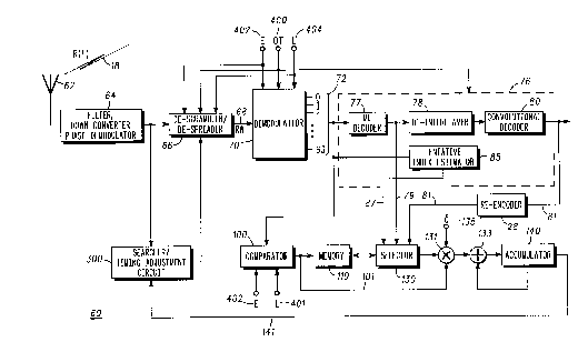
FIG. 4 is a partial block diagram of an apparatus
60 within a base station such as base station 212 (shown
in FIG. 1), for receiving communication signal R(T),
originally transmitted by mobile station 216 as
communication signal S(T) 12. Receiver 60 is preferably
a RAKE receiver having a number of fingers, although
only a single finger is shown. Receiver 60 may be
coherent, non-coherent or quasi-coherent.
CA 022609l8 lgg9-ol-l9
WO 98/05141 PCT/US97/08568
Antenna 62 receives communication signal R(T) 18,
which comprises a number of received frames. Front-end
processing such as filtering, frequency down-converting
and phase demodulation of communication signal R(T) 18
is performed by well-known methods and circuits at block
64 .
Searcher 300, the operation and construction of
searchers being generally well-known, attempts to lock
onto received signal R(T) 18 at approximately the time
of reception of R(T) 18, looking for R(T) 18 at a
plurality of time offsets. Once receiver 60 has locked
onto signal R(T) 18 at the time offset which
approximates the ideal time of reception of R(T) 18,
referred to as on-time offset OT 400, receiver 60 may
also monitor R(T) 18 at a time offset slightly earlier
than OT 400, referred to as early offset ~ 402, and at
a time offset slightly later than OT 400, known as late
offset L 404. Early offset E 402 and late offset 404
are preferably approximately one Walsh chip period
apart.
At each time offset 400, 402 and 404, de-
scrambler/de-spreader block 66, among other things,
removes the PN code applied by scrambler block 44 (shown
in FIG. 2) to the series of Walsh codes W 39 (also shown
in FIG. 2). In the IS-95 reverse-link channel, a
received frame of received signal 18 includes ninety-six
received symbols, or Walsh codes, which are each slxty-
four bits long. The received Walsh codes have been
altered during transmission by various channel
parameters, however, and simply appear to receiver 60 to
be received signal samples. Nevertheless, the received
Walsh codes are referred to herein as received Walsh
codes RW.
Referring again to FIG. 4, each received Walsh code
RW 68, after leaving de-scrambler/de-spreader ~6, is
CA 02260918 1999-01-19
WO98/05141 PCT~S97/08568
input to an orthogonal demodulator 70, such as a Fast
Hadamard Transform (FHT). FHT 70 may be implemented
using commercially available hardware as an array of
adders or as a multiplexed adder, depending on its size.
Alternatively, FHT 70 may be implemented utilizing a
conventional digital signal processor (DSP) such as a
Motorola DSP, part no. 56166 or an application specific
integrated circuit tASIC).
Upon receiving a received Walsh code RW 68, FHT 70
generates a number of output signals 72. Outputs 72
associated with the received Walsh code RW 68 input to
FHT 70 at early offset time E 402 are referred to as the
set of early outputs, outputs 72 produced by FHT 70 in
response to the received Walsh code 68 at on-time offset
time OT 400 are referred to as the set of on-time
outputs, and outputs 72 associated with late offset time
L 404 are referred to as the set of late outputs.
Sixty-four output signals 72 are generated by FHT
70 per Walsh code RW 68. Each output signal 72 has an
index which references one of the sixty-four possible
Walsh codes W 39 generated by M-ary orthogonal modulator
36 (shown in FIG. 2). Thus, in the IS-95 reverse link
channel, when a received Walsh code group RW 68 is input
to FHT 70, sixty-four output signals 72 which correlate
to sixty-four possible transmitted Walsh codes 39 are
produced. It should be understood that in addition to
having an index, each output signal 72 also has an
associated complex number (not shown). Seven bits are
preferably allocated to the real and imaginary portions,
respectively, of the complex number, although fewer or
more bits are possible. For simplicity, the index and
the complex number will be referred to collectively as
output signal 72.
Each output signal 72 further has an associated
energy value (not shown), commonly calculated by
CA 022609l8 lgg9-ol-l9
WO98/05141 PCT~S97/08568
--10--
magnitude-squaring the complex number associated with
output signal 72. The energy value generally
corresponds to a measure of confidence, or a likelihood,
that output signal 72 indexes a Walsh code W 39 which
corresponds to a group of received Walsh codes RW 68
input to FHT 70. The energy value may have any suitable
bit width, and may be, for example, fourteen bits wide.
Acting on the set of on-time outputs, decoder block
76, which may include a Maximum Likelihood decoder 77, a
de-interleaver 78 and a convolutional decoder 80,
further demodulates received signal R(T) 18, estimating
transmitted signal 12, and outputting signal 81. After
the demodulation process, re-encoder 28, which may be
substantially similar to encoder 28 shown in FIG. 2, may
re-create the transmitted digitally coded and
interleaved bits, depicted in FIG. 3, which represent
indices to Walsh codes 39. Elements of decoder block 76
may be implemented in a variety of ways. For example,
Maximum Likelihood decoder 77, which estimates indices
to Walsh codes 39, may be implemented in hardware or
software according to well-known methods. Maximum
Likelihood decoders are described in general in J.
~roakis, "Digital Communications", McGraw-Hill, Chapter
6, Section 7 (1983), incorporated herein by reference,
and a description of a Maximum Likelihood decoder for
use in an IS-95A base station receiver may be found in
R. Walton and M. Wallace, "Near Maximum Likelihood
Demodulation for M-ary Orthogonal Signalling", IEEE VTC,
pp. 5-8 (1993), also incorporated herein by reference.
In a first embodiment of the present invention,
comparator 100 accepts the set of early outputs and the
set of late outputs from FHT 70, calculating the
difference between the energy value of at least one late
output from the set of late outputs and the energy value
of at least one early output from the set of early
CA 02260918 1999-01-19
W098/OS141 PCT~S97/08568
outputs. When only one output 72 is selected from both
the set of early outputs and the set of late outputs,
the selected output 72 is preferably the output 72
having an energy value representing the highest measure
of confidence that selected output 72 indexes a Walsh
code 39 which corresponds to the received Walsh code
group RW 68 input to FHT 70. In general, the selected
output 72 from the set of early outputs has a different
index than the selected output 72 from the set of late
outputs. The calculated difference between selected
output 72 from the late output set and selected output
72 from the early output set exits comparator 100 at
line 101. This calculated difference may be represented
by any number of bits, but is preferably represented by
a single bit associated with the sign of the difference,
referred to as a timing measure.
After some additional processing at elements 131,
133 and 140 (discussed further below), the timing
measure is input to searcher/timing adjustment circuit
300, which adjusts on-time offset OT 400 so that
receiver 60 remains locked onto signal R(T) 18 at the
time offset which approximates the ideal time of
reception of R(T) 18 (also discussed further below).
In a second embodiment of the present invention, a
memory 110, which may be a commercially available
random-access memory, for example, may be positioned at
a point within receiver 60 to store timing measures
output from comparator 100 at line 101. A separate
memory 110 is preferably provided for each diversity
element within receiver 60.
Comparator 100 preferably calculates the difference
between the energy values associated with each pair of
corresponding indices in the set of late outputs and the
set of early outputs, storing timing measures resulting
from each of the sixty-four comparisons. Alternatively,
, _ _
CA 022609l8 lsss-ol-ls
WO98/05141 PCT~S97/08568
-12-
memory 110 may store less than all of the sixty-four
timing measures generated by comparator 100 per received
Walsh code 68. For example, memory 110 may retain only
a subset (for example, one or eight or sixteen~ of the
timing measures.
The timing measures may be represented by any
number of bits, but are preferably represented by a
single bit associated with a sign of the calculated
difference. ~or a single power control group in the IS-
95A reverse channel, which includes six received Walsh
codes RW 68, memory 110 may be viewed as a matrix of
timing measures having sixty-four rows and six columns.
Memory 110, however may be smaller or larger, and may,
for example, store timing measures for an entire IS-95A
reverse-channel frame.
Selector 130 preferably receives demodulated signal
81 from decoder block 76, which may have been re-encoded
at re-encoder block 28. Frame demodulation is likely
performed for sixteen power control groups, so that
signal 81 includes ninety-six re-encoded indices 35.
For each of the ninety-six indices 35, selector 130
addresses the appropriate row and column in memory 110
to retrieve the associated timing measure, which may
have been calculated prior to the availability of
demodulated signal 81. After some additional processing
at elements 131, 133 and 140 (discussed further below),
the selected and retrieved timing measure is input to
searcher/timing adjustment circuit 300.
In a first alternative associated with the second
embodiment, Maximum Likelihood decoder 77 may be
operated once per power control group tthat is, for six
consecutive on-time output sets) to produce one set of
"winning" six indices at line 79. For each of the six
indices, selector 130 may address the appropriate row
CA 02260918 1999-01-19
WO98/05141 PCT~S97108568
and column in memory llO to retrieve the associated
timing measure.
In a second alternative associated with the second
embodiment, Maximum Likelihood decoder 77 may be
operated once per power control group to produce a
number of likely sets of six indices at line 79. For
each diversity element, such as a RAKE receiver finger,
the selected sets of indices are combined, and an
overall most likely set is produced. A channel
correction may also be applied to the selected sets of
indices prior to combining. A suitable method for
channel correction is disclosed in U.S. Patent
Application Serial No. 08/582,856, entitled "Method and
Apparatus for Coherent Channel Estimation in a
Communication System, assigned to the assignee of the
present invention and incorporated herein by reference.
The resulting set of indices set has the highest
likelihood of representing the transmitted indices, and
is used to address the appropriate rows and columns in
memory llO to retrieve the associated timing measures.
In a third alternative associated with the second
embodiment, a set of on-time outputs may be input to
tentative index estimator box 85, which combines the on-
time energy values of corresponding indices from each
diversity element in receiver 60 and outputs the index
having the maximum combined energy value at line 87.
Selector 130 may utilize the output at line 87 to
address memory llO to retrieve the associated timing
measure.
The timing measure(s) output from selector 130 or
comparator lO0 indicate whether on-time offset 400
should be delayed or advanced by searcher/timing
adjustment circuit 300. FIG. 5 illustrates an ideal
time T 408 for receiving a single pulse of R~T) 18. It
can be seen that to approximate ideal time of reception
. _
CA 02260918 lsss-ol-ls
WO98/05141 PCT~Ss7/08568
-14-
T 408, on-time offset OT 400 should be delayed. In
this case, the energy of R(T) at late offset 404 (that
is, output 72 from the late output set) will be greater
than the energy of R(T) at early offset 402 (that is,
output 72 from the early output set), and the
difference, on average, will be positive. The timing
measure will reflect the positive sign of the
difference, indicating that on-time offset OT 400 is
earlier than ideal time of reception T 408, and should
be delayed.
If, on the other hand, on-time offset OT 400 should
be advanced to approximate T 408, the energy of R(T) at
late offset 404 will be less than the energy of R(T) at
early offset 402, and the difference, on average, will
be negative. The timing measure will reflect the sign
of the difference, indicating that on-time offset OT 400
is later than ideal time of reception T 408, and should
be advanced.
If on-time offset OT 400 is correct, the difference
between the energy of R(T) at late offset 404 and at
early offset 402 will, on average, be zero. The timing
measure will be zero, indicating that on-time offset OT
400 should not be changed.
Referring again to FIG. 4, the timing measures
retrieved from memory 110 by selector 130, as well as
timing measures 101, which are both preferably one bit
wide, may be scaled at circuit 131 by a programmable
loop gain a 135, and the resulting product may be summed
at circuit 133 with the contents of a timing measure
accumulator 140. When accumulator 140 reaches a
predetermined positive or negative threshold, a timing
adjustment command may be issued to searcher/timing
adjustment circuit 300 via line 141.
One suitable value of a is three, although the
value of a may be programmable to any other suitable
CA 02260918 1999-01-19
WO98/05141 PCT~S97/08S68
-l5-
value, for example, a value between one and eight. The
signal output from circuit 131 has a bit width equal to
the bit width of ~, which is preferably at least three
bits wide. The bit width at accumulator 140 is
preferably programmable, for example, to three, four or
five bits. In addition, fractional loop gains may be
obtained from the integer loop gains by periodically
switching between gain values. Likewise, a may have an
initial value upon start-up and a different, steady-
state gain thereafter.
One preferred embodiment of a method for receiving
a signal in a digital radio frequency communication
system is outlined in the flowchart of FIG. 6. The
method starts at block 500, and continues to block 502,
where a first step includes inputting, at a first time,
a received symbol associated with a transmitted symbol
to a demodulator to produce a set of early outputs. The
next step, at block 504, includes inputting, at a second
time, the received symbol to the demodulator to produce
a set of on-time outputs. The step of inputting, at a
third time, the received symbol to the demodulator to
produce a set of late outputs is shown at block 505.
The step at block 506 entails comparing at least one
output in the set of early outputs with at least one
output in the set of late outputs to produce a timing
measure. Finally, at block 508, a time for receiving
the signal is adjusted based on the timing measure.
In a second embodiment, the timing measure, which
may be included in a set of timing measures, is stored
in a memory. Next, a predetermined number of outputs in
the set of on-time outputs are input to an estimator
which produces the transmitted symbol. Based on the
transmitted symbol, the timing measure is selected from
the memory. Then, based on the selection, the time for
receiving the signal is adjusted.
CA 02260918 1999-01-19
WO98/05141 PCT~S97/08568
-16-
Although receiver 60 has been described herein in
terms of specific logical/functional circuitry and
relationships, it is contemplated that receiver 60 may
be configured in a variety of ways, such as with
programmed processors or application-specific integrated
circuits (ASICs). It should also be understood that
when one element is responsive to another element, the
elements may be directly or indirectly coupled.
It is contemplated that intermediate decisions
regarding demodulated signal 81, made within decoder
block 76, may be utilized. In addition, demodulated
signal 81 may be re-modulated using, for example, a
circuit such as the circuit depicted in FIG. 2, to
generate spreading sequences. In this manner, FHT
resources may be conserved, and the timing measures may
include more bits.
The IS-95 reverse link channel has been
specifically referred to herein, but the present
invention is applicable to any digital channel,
including but not limited to the forward-link IS-95
channel and to all forward- and reverse-link TDMA
channels, in all TDMA systems, such as Groupe Special
Mobile (GSM), a European TDMA system, Pacific Digital
Cellular (PDC), a Japanese TDMA system, and Interim
Standard 54 (IS-54), a U.S. TDMA system.
The principles of the present invention which apply
to cellular-based digital communication systems may also
apply to other types of communication systems, including
but not limited to personal communication systems,
trunked systems, satellite communication systems and
data networks. Likewise, the principles of the present
invention which apply to all types of digital radio
frequency channels also apply to other types of
communication channels, such as radio frequency
CA 02260918 1999-01-19
WO98/05141 PCT~S97/08568
signaling channels, electronic data buses, wireline
channels, optical fiber links and satellite links.
It will furthermore be apparent that other and
further forms of the invention, and embodiments other
than the specific embodiments described above, may be
devised without departing from the spirit and scope of
the appended claims and their equivalents, and therefore
it is intended that the scope of this invention will
only be governed by the following claims and their
equivalents.