Note : Les descriptions sont présentées dans la langue officielle dans laquelle elles ont été soumises.
CA 02261427 1999-02-09
H6571, b-315
IMPROVED PULSE STEP MODULATOR
The present invention is directed to modulators and, in particular, to pulse
step
modulators which are applicable for use in radio and television broadcasting
systems.
In AM radio broadcasting in the medium-wave and short-wave bands, a high-power
vacuum tube is conventionally used in the final radio frequency amplifier
stage of the
transmitter. For maximum power-amplification efficiency, this tube is not
operated as a
linear amplifier, but rather as a class C or class D biased circuit, producing
an RF envelope
which follows that of the modulation of the RF signal is achieved through
varying the B+ DC
supply voltage provided to the tube anode. Thus, modulation of the RF signal
is achieved
t o through varying the B+dC supply to the plate anode of the tube. The high-
powered audio
amplification circuitry required to vary this voltage is referred to as the
modulator.
Recently, a modulator to achieve the foregoing has been employed as a pulse
step
modulator (PSM) disclosed in the specification of U.S. Patent No. 4,403,197.
Briefly, a pulse
step modulator (PSM) as disclosed includes a plurality of series connected
unit step modules
each of which includes an isolated DC voltage source, a remotely controlled
switch and a
series diode. The switch in each module may be remotely controlled to turn the
module on
or off. As each module is turned on , it provides a step voltage. As the
various modules are
turned on in a stepwise fashion, the output voltage with the maximum equaling
the sum of
all of the module DC voltage sources. A lowpass filter at the output may be
employed for
2o removing switching noise. An encoder or the like monitors a time varying
input signal, and
turns on one of the unit step modules for each incremental increase in the
value of the audio
signal. As the audio signal continues to increase in value, the modules are
sequentially
turned off in the reverse order.
The specification of U.S. Patent No. 4, 560, 944 also discloses a pulse step
modulator .
Such known pulse step modulators include within the isolated DC voltage source
a
transformer means is connected to a rectifier that provides the DC voltage or
step voltage for
the module. There is unwanted or stray capacitance between the transformer
means and
circuit ground. This capacitance limits the switching frequency of the
remotely controlled
switch in the pulse step modulator. The switch in each unit step module is
remotely
3o controlled to turn the module on or off. Each time the module os turned on,
it provides a
step voltage . When the module is turned off the capacitance discharges by way
of the load.
The discharge RC time constant is fixed by the magnitude of the capacitance
and the
magnitude of the load. At high switching frequencies, the unwanted capacitance
becomes a
problem because it limits the system frequency. The switching time may become
so fast that
CA 02261427 1999-02-09
H6571, b-315
the capacitance cannot properly discharge.
Known pulse step modulators have been employed in AM radio broadcasting
applications. It has been proposed to employ such modulators for modulating
the video
signal in a TV broadcasting system. This requires a higher operating
frequency. For
s example, a typical audio frequency application may have an operating
frequency of lOKHz
whereas the symbol rate proposed for high definition television (HDTV)
broadcasting may
well be on the order of 10.76MHz. This is approximately 1,000 times that of
the radio
frequency. Such a high operating frequency will increase the problems
associated with
unwanted or stray capacitance during the switch OFF time. This may result in
video picture
1 o distortion.
An object of the present invention is to provide an improved pulse step
modulator
having means for rapidly discharging the unwanted or stray capacitance in each
module of a
pulse step modulator during the module OFF time.
The present invention includes a pulse step modulator comprising a plurality
of series
is unit step modules, each including a DC voltage source and an associated
actuatable first
switching means for, when on, turning on said associated module to provide a
unit step
voltage, an output circuit connected to said series connected modules to
provide an output
voltage to a load in which the magnitude of the output voltage is equal to the
sum of all the
voltage sources of the modules that are turned on, means for providing a
plurality of module
2o turn on signals, each for turning on said first switching means in none of
said modules for the
time duration of said turn on signal after which said first switching means is
turned off, each
said unit step module including transformer means exhibiting an associated
unwanted
capacitance between said transformer means and circuit ground and which
capacitance
becomes charged when the associated first switching means is turned on, each
said unit step
25 module having capacitance discharge means for rapidly discharging said
associated
capacitance each time said associated first switching means is turned off.
Advantageously an improved pulse step modulator includes a plurality of series
connected unit step modules, each including a DC voltage source and an
associated
actuatable switching means for, when ON, turning on the associated module to
provide a
3o unit step voltage. An output circuit is connected to the series connected
modules for
providing an output voltage s equal to the sum of all the voltage sources of
the modules that
are turned on. A plurality of turn on signals are provided with each serving
to actuate on of
the switches in one of the modules to thereby turn the associated module on.
Upon removal
of the on signal the switching means is turned off and the module is turned
off. Each unit
CA 02261427 1999-02-09
H6571, 6-315
step module includes transformer means that exhibits an associated unwanted
capacitance
between the transformer means and circuit ground. This capacitance becomes
charged when
the associated switching means is turned on. Each module includes capacitance
discharge
means for rapidly discharging the associated capacitance each time the
associated switching
means is turned off.
The present invention will now be described by way of example with reference
to the
accompanying drawings, wherein:
Fig.1 is a schematic-block diagram illustration of a prior art AM broadcasting
transmitter employing a pulse step modulator (PSM);
to Fig. 2 is a schematic-block diagram illustration of a prior art unit step
module
employed in Fig.1;
Fig. 3 is a schematic-block diagram illustration of an improved unit step
module in
accordance with the present invention;
Fig. 4 is a schematic-block diagram illustration of a broadcasting transmitter
employing a plurality of unit step modules with each corresponding to that
shown on Fig. 3;
and
Fig. 5 is a schematic-block diagram illustration similar to that of Fig. 4 but
showing a
plurality of unit step modules on accordance with a second embodiment of the
present
invention.
2o Reference is now made to the drawings in which Fig. 1 illustrates an AM
transmitter
which incorporates a pulse step modulator (1'SM). The transmitter includes an
audio source
10 which generates an amplitude and frequency varying audio signal which is to
be
amplified and transmitted. This signal os supplied by way of a conventional
analog-to-
digital converter 20 to a pulse step modulator (PSM). The pulse step
modulator, to be
described in greater detail hereinafter, amplifies the signal to a high power
level and
provides a resulting amplitude signal to a low pass filter 12. The resulting
amplified and
filtered signal is then supplied to the audio input of a conventional RF power
amplifier 14
where it amplitude modulates an RF carrier signal supplied by an RF oscillator
16. The
resulting AM signal os then transmitted by a conventional antenna 18.
3o The analog-to-digital converter 20 receives the analog audio signal from
the audio
source 10 and converts it into a multi-bit digital representation thereof. For
example, the
analog input signal may be converted into a 12 bit digital signal. The six
most significant bits
(6MSB) are supplied to a encoder 30 having N output circuits which are
supplied to an
optical driver circuit 32. Circuit 32 has N output circuits respectively
connected to N unit
CA 02261427 1999-02-09
H6571, b-315
step switches S1 through SN. Switches S1 through SN are respectively located
in unit step
modules M1 through M(N).
The encoder 30 sequentially energizes its output circuits 1 through N with
incremental increases in the magnitude of the analog signal and de-energizes
the output
circuits in the reverse order with incremental decreases in the magnitude of
the analog signal.
These are reflected through the optical driver circuit 32. The optical driver
circuit has output
circuits 1 through N which serve to sequentially close switches S1 through SN
as the analog
input signal incremental increases in magnitude and to sequentially open the
switches, in the
reverse order, as the input analog signal incremental decreases in magnitude.
Whenever a
to switch S1 through SN is open, the associated unit setup module is turned
off and whenever a
switch is closed, the associated unit setup os turned on.
Each unit setup module M1 through M(N) includes an incremental unit setup
voltage
source V, a switch such as switch S1 and a diode such as D1 all interconnected
as shown with
respect to module M1 in Fig.1. The unit step modules are connected together in
series with
diodes D1 through D(N). Each incremental voltage source may be considered as a
DC
voltage source of a fixed magnitude which, in practice, may be on the order of
600 volts. The
total voltage across the series connected modules os dependent upon the number
of modules
which have been turned on by closure of the associated switches S1 through SN.
For
example, if all of the switches S1 through S(N) are closed, then all of the
unit step voltage
2o sources V are connected together in series and added together to provide an
output voltage
NV. If each unit step voltage source V has a value on the order of 600 volts
and N is on the
order of 50, then the total voltage may be on the order of 30,000 volts.
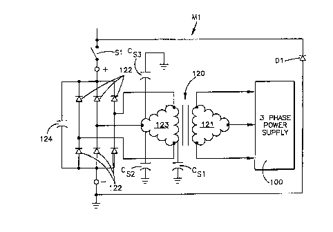
Fig. 2 illustrates one form that module M! of Fig. 2 may take. In this form,
the module
includes in addition to diode D1 and switch S1, a DC voltage source which
includes a 3-
phase AC power supply 100, a transformer 120 having a primary windings 121 and
secondary windings 123 together with six (6) diodes 122 which form a
conventional full wave
3-phase rectifying circuit and a filter capacitor 124. It is to be appreciated
that whereas a 3-
phase supply source and a 3-phase transformer have been illustrated the
circuitry may take
another form.
3o The present invention recognizes that a problem on the operation of pulse
step
modulators is unwanted or stray capacitance associated with the transformer
means. The
capacitance is from the secondary windings to circuit ground and defines the
module to
ground capacitance. This capacitance degrades the operation of the pulse
modulator. It is to
be noted that in a pulse step modulator such as that disclosed in Fig. l, the
load is the
CA 02261427 1999-02-09
H6571,-6-315
mechanism through which the charged capacitance is discharged. The discharge
RC time
constant os fixed by the magnitude of the unwanted or stray capacitance and
that of the load.
This limits the frequency of operation because increased switching frequency
will cause the
switching time to be so fast that the capacitance cannot properly discharge
during the
s module OFF time. This is a particular problem in a substantially higher
frequency
application such as in digital television where the symbol rate may be on the
order 10.76Mhz.
The stray capacitance CS1, CS2, and CS3 from the secondary windings of the
transformer to ground, as well as other stray capacitance between the
transformer and
ground in Fig. 2 are all represented in Fig. 3 by a capacitor CS connected
across the module
to M1 to ground. An additional switch AS1 is connected across the output
circuit of the module
(across the capacitance C~). This switch AS1 is operated so that whenever the
module switch
S1 is open to turn the module OFF the switch AS1 os closed to provide fast
discharge of the
capacitance CS. As illustrated in Fig. 3, this may be achieved by providing a
ganged switch
arrangement so that as switch S1 closes, switch AS1 opens and vice versa.
is Fig. 4 illustrates a pulse step modulator (PSM) system disclosed after the
module M1'
shown in Fig. 3. In this embodiment, the input source 15 may include a low
frequency
source, such as audio source 10 of Fig.1, followed by an analog to digital
converter 20 so that
the output of source 15 is plurality of mufti-bit digital words with each
digital word being
supplied to the encoder 30 as described in Fig. 1. Alternatively, however, the
input source 15
2o may be a digital source such as a stream of digital words obtained from a
video source such
as in a HDTV system. Each digital word in this stream of digital words is
supplied to the
encoder 30 in the manner as described hereinbefore.
The modules M1' through M(n)' take the form as shown in Fig. 3 with respect to
module M1'. Thus as shown in module M1' additional switch AS1 has been added
and
2s operates so that the additional switch AS1 is closed when the module switch
S1 is open and
vice versa. This provides a fast discharge circuit for discharging the
unwanted or stray
capacitance CS associated with the module. As shown in Fig. 4 the additional
switches
include switches AS1, AS2, AS(n-1) and AS(n).
Fig. 5 shows another embodiment of the invention similar to that of the
embodiment
30 on Fig 4 and consequently, like components will be identified herein with
like character
references. In Fig. 5 each module switch and its associated additional switch
are not ganged
together as in Fig. 4 but are made to operate in the same manner by use of the
inverters.
Thus the input signal to switch S1 is either a turn ON signal of a turn OFF
signal. This signal
is applied through an inverter I-1 which inverts the signal for controlling
the additional
CA 02261427 1999-02-09
H6571,.6-315
switch AS1. In this manner when the command to switch S1 is a turn ON command,
the
command to the associated switch ASl is a turn OFF command and vice versa. In
a similar
manner, module M2' in Fig. 5 is provided with an inverter I-2. Also module M(n-
1)' is
provided with an inverter I(n-1). Similarly, module M(n) is provided with an
inverter I(n).
s Advantageously, the various switches are illustrated as being single pole,
double
throw switches they may take various forms such as elecromechanical switches
that are
ganged together in a mechanical manner or they may be electronic switched,
such as various
semi-conductor devices.
A pulse step modulator including a plurality of series connected unit step
modules,
to each with a DC voltage source and an associated actuatable switch for,
turning on the
associated to provide a unit step voltage. An output circuit connected to the
series
connected modules for providing an output voltage to a load, the magnitude of
the output
voltage being equal to the sum of all the voltage sources of the modules that
are turned on.
A plurality of module turn on signals are provided, each for turning on a
switch on one of the
15 modules for the time duration of the turn on signal after which the switch
is turned off. Each
unit step module includes a transformer means exhibiting an associated
unwanted
capacitance becomes charged when the associated switch is turned on. Each unit
step
module has capacitance discharge means.
6