Note : Les descriptions sont présentées dans la langue officielle dans laquelle elles ont été soumises.
CA 02261447 1999-02-11
High isolation optical switch, isolator or circulator having thin film
polarizing
beam-splitters '
Cross Reference to Related Application
This application is a continuation-in-part of US patent application no.
08/694, 415,
filed on August 12, 1996 by Li Li and J. A. Dobrowolski.
Field of Invention
This invention relates to an optical device such as an optical switch, optical
isolator or optical circulator and, more particularly, to a polarization-
independent, high-
isolation optical device that uses a novel thin film polarizing beam-sputter.
Background of the Invention
In fiber telecommunications, and in particular in wavelength division
multiplexing, there is a need for high performance, low-cost and easily-
producible optical
switches, isolators and circulators. Optical switches are used to select fiber
channels
electronically. Optical isolators are commonly used in optical amplifiers that
amplify
fiber signals without using repeating stations. These optical amplifiers are
pumped by
diode lasers, which are very sensitive to any light reflected back to their
cavities. Optical
isolators can be used to isolate any reflected light going back to the lasers.
Recently, optical circulators have become very important in bi-directional
fiber
communications. In a mufti-port circulator, signals go from port 1 to port 2,
port 2 to port
3, port 3 to port 4, and so on, in stead of port 1 to port 2 and port 2 to
port 1. For
example, in Bragg grating wavelength division multiplexers (WDM), without
using a
circulator, the reflected signal would come out from the same port that the
incident light
goes in; as result, the incident light and the reflected light cannot be
physically separated.
However, if a three-port circulator is used, the reflected light will come out
from a
different port. In addition, optical circulators are also used in channel
dropping and
adding from and to main fiber lines.
Typically, an optical device such as an optical switch, isolator or circulator
has a
similar structure. It includes a polarization-rotating device sandwiched
between two
-1-
CA 02261447 1999-02-11
polarizing devices. The first polarizing device is used to separate the
incident beam into
two orthogonal polarized light beams and the second polarizing device is used
to combine
the two orthogonal polarized light beams into one output beam. For a
polarization '
dependent optical switch isolator or circulator, only one polarized light is
used. The
polarization-rotating device normally consists of a reciprocal device or a non-
reciprocal
device, or the combination thereof.
A typical reciprocal device is a waveplate such as a quarterwave plate or
halfwave
plate. A quarterwave plate changes a linear polarized light into a circular
polarized light
if its optical axis is aligned 45° with regard to the polarization of
the incident linear
polarized beam. A halfwave plate rotates the polarization of a linear
polarized light by
any angle depending on the alignment of its optical axis with regard to the
polarization of
the incident beam.
A typical non-reciprocal device is a Faraday rotator. When a magnetic field is
applied to the Faraday rotator, it rotates the electric field of a linear
polarized light by a
certain angle. The rotational angle depends on the property and the length of
the Faraday
rotator as well as the strength of the magnetic field. The direction of the
rotation depends
on the direction of the magnetic field. Therefore, the polarization plane of
the light beam
is rotated in the same direction for light coming from both directions. This
is why such a
device is called non-reciprocal device.
Normally, such an optical device has several input and output ports. For an
optical switch, the output beam is switched between the several output ports
electronically. In order to do this, a mechanism is applied to alter the
direction of the
magnetic field, for example, an electric coil can be used in which the current
can be
switched on in both directions: For an optical isolator, the light comes in
reverse
direction is not used and is directed to a port that is different from the
incident port. To
use as an optical circulator, the signals circulate between all the ports.
Currently, optical switches, isolators and circulators are mainly based on
birefringent polarizing devices such as birefringent polarizers, wedge
polarizers or walk-
off polarizers, for example, US patent nos. 5,446,578 and 5,734,763 by Chang
and US
patent nos. 5,581,640, 5,566,259, 5,557,692, 5,706,371 by Pan et al. Sometimes
-2-
CA 02261447 1999-02-11
absorbing plate polarizers are also used in optical devices which are
polarization-
dependent.
Although birefringent polarizers have the advantage of having high extinction
ratios, there are several disadvantages resulting from their use. First,
birefringent
polarizers are expensive. Second, these polarizers have birefringent effects
that result in
polarization mode dispersion. In order to overcome this problem, other
birefringent
plates or a second identical stage are added to compensate this polarization
dispersion.
Both approaches require the use of more birefringent plates or polarizers, and
this makes
it very expensive and very difficult to assemble since the optical axes of all
the
birefringent elements need to be accurately aligned. Third, the most common
configuration in conventional optical isolators or circulators uses walk-off
birefringent
polarizers to separate ordinary (o) and extra-ordinary (e) rays physically.
This separation
depends on the refractive index difference between o- and e-rays and the size
of the
birefringent material. The greater the separation, the easier it is to package
and the better
the performance. However, since the refractive index differences depend on the
available
birefringent materials which are limited, so an increase in the separation
means an
increase in the size of the birefringent plate. As a result, it is more
expensive because the
greater the size, the more expensive the birefringent materials. Fourth, it is
difficult to
make an N mufti-port optical circulator based on birefringent materials with
the number
of ports N larger than four.
Conventional thin film polarizing devices such as thin film polaxizers or thin
film
polarizing beam-splitters (PBS), including MacNeille polarizers or thin film
cube or plate
polarizers, have been proposed for use as polarizing devices in optical
switches, isolators
and circulators. For example, one example of the optical circulator was
described in US
patent no. 4,272,159 by Matsumoto. The thin film interference polarizers and
PBSs
consist of multilayers of dielectric films deposited onto glass or other
substrates. Such
polarizers reflect s-polarized light and transmit p-polarized light and are
normally based
on the light interference in thin films, sometimes also in combination with
other effects.
Although conventional thin film polarizing devices are versatile in terms of
design
and are not limited by size and are easier to make and hence less expensive,
one of their
-3-
CA 02261447 1999-02-11
biggest disadvantages is the low extinction ratio (less than 30dB isolation),
especially in
the reflected beams. In addition, the bandwidth of the thin film cube or plate
polarizers is
very small. Another disadvantage is that their angular field is very small,
and they
therefore require well collimated light beams. As a result, any optical device
based on
these conventional thin film polarizing devices will suffer the same low
extinction ratio
problem. In addition, they are more difficult to package because of the small
angular
fields. Such optical switches isolators and circulators can only be used in
the areas where
high extinction ratios are not required. For high performance devices, such as
those used
in fiber communications, the market is dominated by the birefringent
materials.
The most commonly used thin film polarizers are the MacNeille polarizes which
was invented by MacNeille in 1946. It is based on the Brewster angle
phenomenon and
light interference in thin films. When light is incident at the interface
between a high and
low refractive index materials, if the incident angle is equal to the Brewster
angle, all the
p-polarized light is transmitted and s-polarized light is partially reflected.
In order to
increase the reflection for s-polarized light, a multilayer interference
coating consisting of
the high and low index materials are used. The coating is sandwiched between
two glass
prisms, which is required by the Brewster angle requirement. The multilayer
coating acts
as a high reflector for the s-polarized light and does not affect the
transmission of the p-
polarized light at the Brewster angle. The reflection band for s-polarized
light depends on
the refractive index ratio of the high and low index materials and can be
extended by
chirping the layer thickness or by using several layer stacks. Hence, the
MacNeille
polarizes is broad band; however, it is very sensitive to the variation of the
angles of
incidence. Once the incident angle moves away from the Brewster angle
(~2°), the
performance of the polarizes deteriorates dramatically. In addition, the
extinction ratio
for the reflected beam is low because the index-mismatch between the prism
substrate
and the coating materials.
Another thin film PBS (polarizing beam splitter) is based on the edge
separation
between s- and p-polarized light of an edge filter at an oblique angle of
incidence. In this
separation region, s-polarized light is reflected and p-polarized light is
transmitted. Its
angular field is relatively large compared to MacNeille polarizes. The
extinction ratio of
such polarizes can be very high in the transmitted beam if a large number of
layers are
-4-
CA 02261447 1999-02-11
used to reflecting s-polarized light. However, a high extinction ratio can not
be achieved
for the reflected beam. In addition, such a polarizer has a very small
bandwidth. As a
result, it is often used for narrow band applications such as lasers.
It is therefore an object of the present invention to provide a low-cost, high
isolation and polarization-independent optical device that can be used as an
optical
switch, isolator or circulator.
Summary of the Invention
In its most general aspect the invention provides an optical device for
controlling
the flow of light between ports, comprising a pair of thin film polarizing
devices, the
improvement wherein said thin film polarizing devices employ frustrated total
internal
reflection and interference in a thin film coating to transmit s-polarized
light and to reflect
p-polarized light.
It will be understood by one skilled in the art that a thin film coating
typically
consists of multilayers formed on a substrate.
Typical thin film polarizing devices are polarizers or polarizing beam
sputters
(PBS). It will be understood that depending of the direction of light, such
polarizing
devices can be used to split unpolarized light into separate s- and p-
polarized beams or to
combine such separately polarized beams into a single unpolarized beam. The
term
polarizing device in this specification covers such devices whether
functioning as beam
splitters or beam combiners. Several parameters that are used to describe the
performance of a polarizing device are:
1. the wavelength range, which is the range over which the polarizing device
is
effective;
2. the angular field, which is the angular field of the incident light in
which the
polarizing device is effective;
3. the extinction ratio, which is the ratio of the desired polarized light to
the
unwanted polarized light after the light passes through or is reflected from
the
polarizing device; and,
-5-
CA 02261447 1999-02-11
4. the transmittance or reflectance for the desired polarization.
Polarizing devices employed in the invention are non-absorbing, and have
broadband wavelengths, wide angular fields and high extinction ratios, also
are easier and
less expensive to manufacture. In a typical application, one polarizing device
functions as
a beam sputter to split incident unpolarized light into separate s- and p-
polarized beams
and the other polarizing device functions to combine the beams into a single
unpolarized
beam. A polarization-rotating device, which may be either reciprocal or non-
reciprocal,
may be placed in the respective p- and s- polarized beams. Such an arrangement
can be
used to make multi-port optical switches, isolators or circulators.
In a preferred embodiment, wherein in a first direction a first of the
polarizing
devices splits a light beam incident at a first port into a reflected p-
polarized beam and a
transmitted s-polarized beam, and a second of said polarizing devices combines
ap-
polarized beam and a s-polarized into a combined unpolarized output beam at a
second
port. A polarization-rotating device, such as a Faraday rotator, can be
inserted in the
beams to control the flow of light between the ports and thus create optical
switches,
isolators or circulators. Such devices do not have polarization mode
dispersion if a
symmetrical configuration is used. The insertion loss in these devices can be
small as
well. The optical device can also be made polarization dependent, in which
case only one
polarized beam is used. A single polarizing device directs incident polarized
light through
the input port of a polarization-rotating device to a reflecting surface, from
where it is
reflected back into the polarizing device, with its plane of polarization
changed. The
reflected beam appears at an output port.
Brief Description of Drawings
The invention will now be described in more detail, by way of example, with
reference to the accompanying drawings, in which:
Fig. 1 shows a typical configuration of the novel thin film polarizing device
disclosed in US patent application no. 08/694, 415;
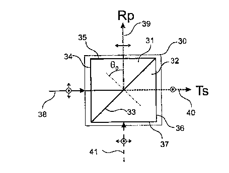
Fig. 2 shows the configuration of the first PBS embodiment;
Fig. 3 shows the configuration of a variation of the first PBS embodiment;
-6-
CA 02261447 1999-02-11
Figs. 4a and 4b show the calculated transmittance and reflectance of a
polarizing
beam-sputter coating (PBS-1 A) at different angles of incidence for the first
PBS
embodiment;
Figs. Sa and Sb show the calculated transmittance and reflectance of a
polarizing
beam-sputter coating (PBS-1B) at different angles of incidence for the first
PBS
embodiment;
Fig. 6 shows the configuration of the second PBS embodiment;
Figs. 7a and 7b show the calculated transmittance and reflectance of a
polarizing
beam-sputter coating (PBS-2) at different angles of incidence for the second
PBS
embodiment;
Fig. 8 shows the configuration of the third PBS embodiment;
Figs. 9a and 9b show the calculated transmittance and reflectance of a
polarizing
beam-sputter coating PBS-3 at different angles of incidence for the third PBS
embodiment;
Fig. 10 shows the configuration of the fourth PBS embodiment;
Figs. l la and l lb show the calculated transmittance and reflectance of a
polarizing beam-splitter coating PBS-4 at different angles of incidence for
the fourth PBS
embodiment;
Fig. 12 illustrates the principle of operation of a polarization-rotating
device used
in an optical device in accordance with the present invention;
Figs. 13a and 13b are cross sectional views, and Fig. 13c is a schematic
diagram
showing the working principle, of an optical device in accordance with a first
embodiment of the invention;
Figs. 14a and 14b are cross sectional views, and Fig. 14c is a schematic
diagram
showing the working principle, of the second embodiment of an optical device
in
accordance with the principles of the present invention;
CA 02261447 1999-02-11
Figs. 15a and 15b are cross sectional views, and Fig. 15c is a schematic
diagram
showing the working principle, of the third embodiment of an optical device in
accordance with the principles of the present invention;
Figs. 16a and 16b are cross sectional views, and Fig. 16c is a schematic
diagram
showing the working principle, of the fourth embodiment of an optical device
in
accordance with the principles of the present invention;
Figs. 17a and 17b are cross sectional views, and Fig. 17c is a schematic
diagram
showing the working principle, of the fifth embodiment of an optical device in
accordance with the principles of the present invention;
Fig. 18a and 18b shows the configuration of a polarization isolator using a
single
polarizing device; and
Fig. 19 is an in-depth perspective view of the PBS embodiments that can be
used
in mufti-port optical devices in accordance with the present invention.
Detailed Description of the Invention
The optical device described herein uses a novel thin film polarizing device
disclosed in US patent application no. 08/08/694, 415, filed on August 12,
1996 by Li Li
and J. A. Dobrowolski and also in a paper by Li Li and J. A. Dobrowolski
presented in
June 1998 at the Topical Meeting on Optical Interference Coatings.
Fig. 1 shows a typical configuration of the novel thin film polarizing device.
The
thin film polarizing coating 10 consists of a stack of alternate low and high
refractive
index layers 10a, l Ob sandwiched between two high refractive index substrates
12 and 14.
This novel thin film polarizing device is based on the effects of the
frustrated total
internal reflection and light interference in thin films as more fully
described in the above
patent application, the contents of which are incorporated herein by
reference.
The incident angle ~ in the prism is larger than the critical angle for the
low index
layers. Unlike conventional thin film polarizers or PBSs, this thin film
polarizing device
reflects p-polarized light and transmits s-polarized light. More importantly,
the polarizing
device is at the same time non-absorbing, broad band, wide-angle and it has
very high
extinction ratios (several orders of magnitude higher than conventional thin
film PBSs)
_g_
CA 02261447 1999-02-11
and high transmittance and reflectance for the desired polarization. The
theory of such a
polarizing device has been explicitly described in US patent application no.
08/694, 415
and in the paper by Li Li and J. A. Dobrowolski, which is herein incorporated
by
reference.
Theory of the Novel Thin Film Polarizing Device
Since the thin film polarizing device can function either as a beam-sputter or
beam-combiner as explained above already, this functionality does affect the
theory of the
thin film polarizing device. In the following section, for simplicity, the
term thin film
polarizing beam-splitter (PBS) is used to refer to the thin film polarizing
device instead.
It is understood that both terms are interchangeable.
a. Equivalent Layer Concept
The theory of the novel thin film polarizing beam-splitter can be derived with
the
help of the equivalent layer concept.
Mathematically, a symmetrical thin film structure ~ dl (A) d2(B) dl(A) ~ can
be
replaced by a single layer with an equivalent admittance E and an equivalent
phase
thickness T. Here, A and B represent two different layers with refractive
index n~ and
n2, and thickness dl and dz, respectively. As a result, a multilayer system no
~ [d~(A)
d2(B) d~ (A)]N ~ no can then be replaced by no ~ (E, Nl~ ~ no. Here N is the
number of
periods. The analytical equations for both the E and Tat normal incidence were
described in the book, "Applied Optical Thin Films" by J. F. Tang in Equation
(1).
rl; (sin28,cos8z+~(ylr~z+r~zlrl,)cos2~,sin~z-2(r~,lr~z-rlzlrl,)sin8z)
E -
(sin 28, cos b~z + ~ (r~, l rlz + rlz l r~, ) cos 28, sin ~Z + ~ (rl, l ~z y z
/ r~, ) sin ~z ) ( 1 )
I' = arccos(cos 2b', cos 8z + ~ (r~, l r~z + rlz l rl, ) sin 28, sin 8z )
Where,
-9-
CA 02261447 1999-02-11
~, _ ~ n,d, cos B,
(2)
b'z = ~ nzdz cosBz
Equation ( 1 ) can also be applied to non-normal incidence by replacing r~~
and rh
with Equation (3):
X70 = ~7os = ~o cos Bo X70 = ~7oP = no / cos B°
r~, = r~,s = n, cos B, (s - pol) , r~, = r~, p = n, / cos B, (p - pol) (3)
~7z = rl2s = nz cos Bz ~7z = ~7zP = nz / cos Bz
S Where ~, B, and Bz are the incident angles in the substrate no and in the
high and
low index layers with refractive indices nl and n2, respectively.
b. Simplified Equations for the Equivalent Layer
If the layers are very thin, for example, d~ and d2 are small, then
cos(8, ) =1 sin(, ) - 8,
cos(8z ) -1' sin(8z ) - ~z (4)
Equation (1) can be modified for both s- andp-polarized light as:
2d,(n,z -n°z)+dz(nzz -n°z) +n z cost B
s (2d, + d z ) ° ° (5)
rs =arccos(1-4~zd,dz(n,z -nzz))
__ (2dn,z +dznzz)n,znzz
EP (2d, +dz)n,znzz -(2d,nzz +dzn,z)n°z sinz Bo)
z z (6)
n n
4~zd,dz((n~z -nzz)-( 'z -?z )noz sinz S~°)
I'P = arccos(1- ~ nz n' )
- 10-
CA 02261447 1999-02-11
2 2 2 2
In Equation (5), if 2d, (n, - no ) + d z (nz - no ) = 0 , then
(2d, + d z )
(n'z noz) ( )
dz = z z Zd, 7
(no - nz )
Replace d2 in Equation (5):
( z _ z) ( z _ z)
Es = 2d, n, no + d z nz no + noz cos z Bo = no cos Bo = Los
(2d, +dz)
(8)
8~czd,z(n,z -noz)(n,z -nzz)
>,s = arccos 1-
z n z-n z
(o z)
The above results indicate that ES matches r~s completely. Therefore, the
symmetrical structure behaves like a perfect antireflection coating for s-
polarized light. It
transmits all s-polarized light independent of wavelengths and angles of
incidence. The
equivalent phase thickness is a function of dl, no, n~, n2 and the wavelength
~,.
From the above equation, it is obtained that,
2 2
d z = (n' z n° z ) 2d, (9)
(no - nz )
As long as nl<-no<_n2 or n2<_rao<-n,, there is always a non-negative solution
for dz.
Forp-polarized light, replaced d2 with equation (9), EP and hP in equation (6)
can
be simplified as:
z z z
E - + no n.~ nz (10)
n,2n2z -(n,z +nzz -n°z)n°Z Slriz B°
z z
87tzd,z(n,z -nzz)(n,z -noz)(1-(n' z n2 )noz slnz 90)
1 S TP = arccos(1- z z z ' nz ) ( 11 )
~ (no - nz )
Since not n,z n2z is always greater than zero, if
n,znzz -(n,z +nzz -noz)noz slnz Bo < 0 (12)
-11-
CA 02261447 1999-02-11
EP will have an imaginary value and a negative sign should be chosen in front
of
equation (10).
From equation ( 12), we obtain:
z
n' z z > n' = sin 9~ , if n, < no < nz
noz(1 _ no zy ) no
z n~znzz nz
sin Bo > z z z z -
no (n~ + nz - no ) n z n
z z z > ? = sin B~, if nz < no < n,
noz (1 _ no znz ) no
n~
S where ~ is the critical angle defined as the above equation. Therefore,
there
exists a lower-limit angle 6~,L is defined as:
no sinBLl = n' z (13)
(nlz + nzz - noz)
As long as ~ is larger than 6~,L and smaller than 90°, the condition of
a negative
imaginary EP is always satisfied. A negative EP means that the symmetrical
thin film
structure acts like a perfect metal, it always reflects p-polarized light.
There is no
absorption. The actual reflectance depends on the absolute value of EP and TP.
If the
symmetrical thin film structure is thick enough, virtually all thep-polarized
light is
reflected, no p-polarized light is transmitted.
Therefore, the conditions are obtained for the design of a broadband, wide
angle
and high extinction ratio polarizing beam-sputter. The two most important
conditions are
described in equations (9) and (13) that give the insight on how to select
thin film coating
parameters and the design angles for the novel thin film polarizing beam-
sputter. In the
actual thin film polarizing beam-sputter design process, an initial design is
first obtained
from the above two equations. Then a thin film computer optimization procedure
is used
to optimize the thickness of each individual layer according to the specified
performance
requirements. As a result, the actual coating designs might not be symmetrical
anymore.
In addition, the thickness might be changed as well and they could be rather
thick.
- 12-
CA 02261447 1999-02-11
Embodiments of Thin Film PBSs
Several thin film PBS embodiments having thin film PBS coatings PBS-lA, PBS-
1B, PBS-2, PBS-3 and PBS-4 have been designed for an optical device, such as
an optical
switch, isolator or circulator in accordance with the present invention. For
comparison, the
S designed wavelength range is kept between 1450 - 1650nm for all thin film
PBS coatings.
The extinction ratios for both transmitted and reflected beams are also kept
close to or better
than 10:1. In other words, the isolation for the undesired polarization is
close or better than
60dB. The thin film PBS coatings are mostly based on the optical constants
published in the
book, "Optical constants of Solids I" and "Optical Constants of Solids II",
edited by E. Palik,
and published in 1986 and 1991, respectively. Some measured optical constants
of some
materials by the inventor's laboratory are also used. The initial thin film
PBS coatings were
obtained from equation (9) and (13). Afterwards, the thicknesses of the
coatings were
optimized according to the specified performance requirements. The final
parameters of all
the thin film PBS coatings are listed in Table 1 below.
The center design angle ~ in the above PBS embodiment is 45°. This
arrangement
is desirable because it results in the minimum prism size for a given size of
the accepting-
surface. However, it requires the use of high index materials. According to
equation (13), if
the coatings materials are chosen to be Si and Si02, the substrate material
has to have a
refractive index higher than the refractive index of Si02 but smaller or equal
to the refractive
index of Si.
A variation of the first PBS embodiment 48 is shown in Fig. 3 and Fig. 19AA.
The
center design angle ~ is also 45°. It consists of all the similar
elements as in the first PBS
embodiment. However, in stead of using two right angle prisms, two identical
parallel thick
plates 50 and 51 forming a rhomboidal prism are used. The thin film PBS
coating 33 lies
between the two thick plates 50, 51. An unpolarized light beam 49 is separated
into two
polarized beams by the thin film PBS coating 33. Thep-polarized light is first
reflected by
the thin film PBS coating and then totally reflected by the surface 52 because
the incident
angle at this surface is larger than the critical angle. As a result, the p-
polarized light exits
the light-accepting surface 53 parallel to the incident beam 49. The s-
polarized light is
transmitted by the thin film PBS coating and exits the light-accepting surface
54 in the same
-13-
CA 02261447 1999-02-11
direction as the incident beam. For the unpolarized light beam 56, it is first
totally reflected
by the surface 55 and then is incident upon the thin film PBS coating and goes
through a
similar process as the light beam 49. Such a PBS configuration is desirable in
some optical
device embodiments in accordance with the present invention.
The two thin film PBS coatings PBS-lA and PBS-1B can be used in the first PBS
embodiment as shown in Fig. 2 and its variation as shown in Fig. 3. PBS-lA
consists of 17
layers of Si and Si02 materials and is based on a Si substrate. PBS-1B
consists of 25 layers
of Si and Si02 materials and is based on a ZnSe substrate. The wavelength
region is from
1450nm to 1650 nm. The angular fields in the prism for both PBS-lA and PBS-1B
is
45°~3°, which correspond to ~10° in air for PBS-lA is
~7° in air for PBS-1B respectively.
The calculated transmittance and reflectance of PBS-lA at different angles of
incidence are
plotted in Figs. 4a and 4b. The calculated transmittance and reflectance of
PBS-1B at
different angles of incidence are plotted in Figs. Sa and Sb. Both thin film
PBS coatings
have similar extinction ratios of 106:1. The undesired polarization is
attenuated by more
than 60 dB. Clearly, these extinction ratios are much better than those of
conventional thin
film polarizing devices that could only achieved less than 30dB attenuation
for the undesired
polarization. PBS-lA consists of fewer layers than PBS-1B because the
refractive index of
the Si substrate is higher than that of the ZnSe substrate.
If a lower refractive index substrate is used, or the design angle ~ is
increased on
purpose in order to simplify the thin film PBS coating, a second PBS
embodiment 60 can be
used as shown in Fig. 6 and Fig. 19B. This embodiment, which employs a split
hexagonal
prism, preserves the perpendicular or parallel arrangements for the incident
and output
beams, but allows the angle of incidence ~ greater than 45° at the thin
film PBS coating 65
in the prism. This can be done by shaping the angles of the light-accepting
surfaces 61, 62,
63, 64, with regard to the plane of the thin film PBS coating . The incident
beams or output
beams are not normal to the light accepting surfaces anymore, but strike with
a small angle
of incidence. The four light-accepting surfaces normally have anti-reflection
coating in
order to remove any reflected light.
The thin film PBS coating PBS-2 can be used for the second PBS embodiment. The
center design angel ~ is SS°. PBS-2 consists of 19 layers made of the
same coating and
-14-
CA 02261447 1999-02-11
substrate materials as PBS-1B (Table 1 below). The calculated transmittance
and reflectance
at different angles of incidence are plotted in Figs. 7a and 7b. As it can be
seen, the
performance of PBS-2 is compatible to PBS 1B. However, PBS-2 consists of only
19
layers, compared to 25 layers in PBS-1B. The total metric thickness is about
2060.3nm, also
S less than 3218.1nm of the PBS-1B. This is beneficial from the manufacturing
point of view,
because it requires less time to deposit the PBS-2 coating.
Table 1 Parameters of Thin Film PBS Coatings
PBS-lA PBS-1B PBS-2 PBS-3 PBS-4
No. of 17 2S 19 25 23
La ers
Total 1950.9 3218.1 2060.3 6241.6 5429.5
Thickness
nm
Systems Mat.Thick Mat. Thick Mat. Thick.Mat. Thick.Mat. Thick
nm nm mn nm nm
Sub. Si _ ZnSe _ ZnSe
F4 F4
Si0 14.1 Si0 71.9 Si0 48.2 Nb 43.7 Nb 40.2
O OS
Si 152.2 Si 57.5 Si 63.9 Si0 262.4 SiOz 233.3
Si0 S7.S Si0 198.5 Si0 146.7Nb 131.5 Nb 107.9
OS OS
Si 145.8 Si 58.2 Si 88.0 Si0 419.3 SiOz 263.8
Si0 109.0 Si0 272.5 Si0 159.3Nb 142.6 Nb 119.4
OS OS
Si 141.6 Si 50.4 Si 103.5Si0 486.5 Si0 399.7
Si0 140.4 Si0 268.6 Si02 140.2Nb 130.2 Nb 160.4
OS OS
Si 140.1 Si 39.8 Si 109.1Si0 451.7 SiOz 481.4
Si0 149.9 Si02 229.6 Si0 164.2Nb 115.7 Nb 173.7
OS O
Si 140.1 Si 38.6 Si 93.8 Si0 459.7 SiOz 408.3
Si0 140.4 Si0 239.2 Si0 201.5Nb 117.8 Nb 181.4
OS OS
Si 141.6 Si 31.9 Si 85.7 Si0 454.5 Si0 327.6
Si0 108.9 Si0 167.8 Si0 194.0Nb 112.8 Nb205174.1
OS
Si 145.8 Si 32.2 Si 77.6 Si0 463.0 Si0 386.3
Si0 57.5 Si02 236.9 Si0 139.8Nb 120.1 Nb 168.8
OS O
Si 152.2 Si 38.1 Si 58.4 Si0 473.5 Si0 471.2
Si0 14.1 Si0 217.4 Si0 97.8 Nb 122.6 Nb20 159.5
O
Si 39.1 Si 48.4 Si0 458.6 SiOz 400.7
Si0 256.6 Si0 40.1 Nb 129.3 Nb 120.4
OS OS
Si 50.8 SiOz 406.5 SiOz 268.2
SiOz 256.8 Nb 119.8 Nb205108.6
OS
Si 58.9 Si02 289.2 Si0 234.1
Si0 184.6 Nb 97.8 Nbz0540.2
OS I
Si 56.6 Si0 197.7
Si0 65.7 Nb205 35.2
Sub. Si ZnSe ZnSe SF4 SF4
If an even lower refractive index substrate has to be used, or the design
angle ~ has
to be increased on purpose even more in order to simplify the thin film PBS
coating, a third
-15-
CA 02261447 1999-02-11
PBS embodiment 80 can be used as shown in Fig. 8 and Fig. 19C. It consists of
similar
elements as the first PBS embodiment. The angle of incidence ~ is greater than
45°. The
incident beams 81, 82 and the output beams 83, 84 are normal to the light
accepting surfaces
85, 86, 87, 88 respectively. This can be done by shaping the angles of the
light-accepting
S surfaces 85, 86, 87, 88 with regard to the plane of the thin film PBS
coating 89. The incident
beam or output beams are normal to the light accepting surfaces. The four
light-accepting
surfaces are normally anti-reflection coated in order to remove any reflected
light from these
surfaces.
The thin film PBS coating PBS-3 can be used for the third embodiment. The
center
design angel ~ is 70°. PBS-3 consists of 25 layers of Si02 and Nb205
materials and is based
on the SF4 glass substrate (Table 1 ). The calculated transmittance and
reflectance of PBS-3
are plotted in Figs. 9a and 9b. The extinction ratio is about 106:1 for most
angles of
incidence. This is compatible to the above thin film PBS coatings. However,
because the
refractive indices of the substrate and the high index materials are lower,
the angular field of
PBS-3 is about 70°~2° in prism and ~3.4° in air, smaller
than the above thin film PBS
coatings. However, compared to conventional thin film polarizing devices, this
angular field
is still much better.
For some optical device embodiments in accordance with the present invention,
it is
desirable to have the incident beams and output beams parallel to each other.
This can be
realized in the fourth PBS embodiment 100 as shown in Fig. 10 and Fig. 19D.
The
embodiment consists of similar elements as the first PBS embodiment. The angle
of
incidence ~ at the thin film PBS coating 109 is much greater than 45°.
The incident beams
101, 102 and the output beams 103, 104 are incident upon the light accepting
surfaces 105,
106, 107 and 108 at an angle. This angle will result in the incident beams
inside the prism
meet the requirements for the thin film PBS coating design. The four light-
accepting
surfaces are anti-reflection coated in order to remove any reflected light
from these surfaces.
The thin film PBS coating PBS-4 can be used for the fourth embodiment. The
center
design angel ~ is 75°. PBS-4 consists of 23 layers of SiOz and Nb205
materials and is based
on the SF4 glass substrate (Table 1). The calculated transmittance and
reflectance of PBS-4
are plotted in Figs. 11 a and 11 b. The extinction ratio is about 10':1 for
most angles of
- 16-
CA 02261447 1999-02-11
incidence. This is compatible to the above thin film PBS coating PBS-3. The
angular field
is about 75°~2° in prism and ~3.4° in air.
Clearly, without departure from the spirit of the invention, other thin film
polarizing device embodiments having different wavelength bandwidths, angular
fields,
extinction ratios, as well as using different coating and substrate materials
can be
designed. This has been fully demonstrated in the patent application no.
08/694, 41 S filed
on August 12, 1996 by Li Li and J. A. Dobrowolski.
Embodiments of Optical Devices
The embodiments of the optical device, such as an optical switch, optical
isolator or
optical circulator in accordance with the present invention comprises of at
least one thin film
polarizing device of the type described in the above section and at least a
polarization-
rotating device.
The polarization-rotating device 120 consists of a reciprocal device such as a
Faraday rotator 122 and a halfwave plate 124 (Fig. 12). A magnetic field is
applied to the
Faraday rotator in the z-direction. This can be achieved by using a permanent
magnet or
an electric coil with electric current passing through. When the light
polarized in the y-
direction travels in the forward direction (z-direction), the Faraday rotator
rotates the
polarization of this linear polarized light by 45° in the counter-
clockwise direction if
looking into the z-direction. When the rotated polarized light passes through
the
halfwave plate 124, its plane of polarization is rotated 45° in the
opposite direction with
regard to the first rotation by the Faraday rotator. Therefore, the
polarization rotation is
completely cancelled out and the light comes out from the polarization-
rotating device
with its polarization unchanged in the y-direction. For light linearly
polarized in the x-
direction, it also keeps its polarization state unchanged after passing
through the
polarization-rotating device in the forward direction. However, when linear
polarized
light travels in the reverse direction, the polarization rotations by the
halfwave plate 124
and by the Faraday rotator 122 are in the same direction; as a result, linear
polarized light
in y-direction becomes linear polarized in x-direction and linear polarized
light in x-
direction becomes linear polarized light in y-direction. This non-reciprocal
effect is
extensively used in optical isolators and circulators.
-17-
CA 02261447 1999-02-11
If the magnetic field is reversed in the opposite direction, the polarization
rotation
will be reversed as well for light travel in the forward and reverse
directions. In other
words, the polarization of a linear polarized light will be rotated by
90° in the forward
direction and 0° in the reverse direction.
The first embodiment of the optical device in accordance with the present
invention is shown in Figs. 13a to 13c. It consists of two polarizing devices
130 and 132
such as the first PBS embodiment, two polarization-rotating devices 134, 136
and two
mirrors 138, 139. It has four ports P1, P2, P3, P4 and four light beams can be
incident or
exit from these ports. For an unpolarized light beam incident at port P 1, the
p-polarized
light is first reflected by the polarizing device 130 and then by the mirror
138. After
passing through the polarization-rotating device 134, its polarization is
unchanged and
therefore it is reflected by the second polarizing device 132 and exits from
the port P2.
For the s-polarized light, it is first transmitted by the first polarizing
device 130 and then
passes through the polarization-rotating device 136 with its polarization
unchanged and
then is reflected by the mirror 139 towards the second polarizing device 132.
Therefore,
it is transmitted by the polarizing device and exits from port P2. As a
result, all incident
light at port P 1 goes to port P2 independent of the polarization. Unpolarized
light
incident at port P3 will go through similar routes and come out from port P4.
If the magnetic filed is reversed electronically (for example if an electric
coil is
used to generate the magnetic field, this can be easily done by reversing the
current
direction), the polarization rotations by the halfwave plate and Faraday
rotator will be
accumulated in the forward direction and be cancelled out in the reverse
direction. As a
result, the unpolarized light from port P 1 can come out from either port P2
or port P4
depending on the direction of the magnetic field. Therefore this optical
device can be
used as an optical switch. This mode of operation is present in all optical
device
embodiments in accordance with the present invention. It will not be
explicitly
mentioned again as it has been clearly demonstrated here.
When a polarized light travels in the reverse direction from port P2, the p-
polarized light is first reflected by the polarizing device 132 and then its
polarization is
rotated by 90° by the polarization-rotating device 134. As a result, it
becomes s-polarized
-18-
CA 02261447 1999-02-11
light and is transmitted by the polarizing device 130 and exits from port 3.
The s-
polarized light from port P2 becomes p-polarized light after passes through
the
polarization-rotating device 136 and is reflected by the polarizing device 130
and
eventually exits from port P3. Therefore, all light from port P2 goes to port
P3, similarly,
all light from port P4 goes to port P1. As a result, this optical device
circulates optical
signals from port P 1 to port P2, port P2 to port P3 and port P3 to port P4
and port P4 to
port P1 as shown in Fig. 13c. It is, therefore, an optical circulator.
If port P3 and port P4 are not connected to any optical signals, the device
can be
used as an optical isolator. Light can travel in the forward direction from
port P1 to port
P2. However, any light from port P2 is directed to port P3 which is physically
isolated
from port P 1. This mode of operation is present in all optical device
embodiments in
accordance with the present invention and therefore will not be explicitly
mentioned
again as it has been demonstrated here.
The second embodiment of the optical device in accordance with the present
invention is shown in Figs. 14a to 14c. The working principle of this
embodiment is
exactly the same as the first optical device embodiment. However, it uses two
polarizing
devices 140 and 142 similar to the PBS embodiment 48 shown in Figs. 3 and
19AA,
which is the variation of the first PBS embodiment 30. One advantage of such
PBS
embodiment is that it simplifies the structure of the optical device by
combining the
polarizing device with a mirror. Another advantage is that all incident beams
and output
beams are parallel to each other which is desirable in some applications. Like
the first
embodiment of the optical device, two polarization-rotating devices 144, 146,
consisting
of a Faraday rotator and a halfwave plate are inserted in each polarized beam,
respectively.
The third embodiment of the optical device in accordance with the present
invention is shown in Figs. 1 Sa to 15c. It is similar to the first optical
device embodiment.
It consists of two thin film polarizing devices 1 S0, 152, two mirrors, 158,
159 and two
polarization-rotating devices 154, 156. The incident beams and output beams
are either
perpendicular to or parallel to each other. The two polarizing devices 150,
152 are similar
-19-
CA 02261447 1999-02-11
to the second PBS embodiment 60 shown in Figs. 6 and 19B in which the incident
angle
in the prism is larger than 45°.
The fourth embodiment of the optical device in accordance with the present
invention is shown in Figs. 16a to 16c. It consists of two thin film
polarizing devices 160,
162, two mirrors, 168, 169 and two polarization-rotating devices 164, 166. It
is also
similar to the first optical device embodiment. However, the angle of
incidence in the
prism is larger than 45° and it uses the third PBS embodiment 80 shown
in Figs. 8 and
19C. In addition, the incident beams and output beams are not perpendicular or
parallel
to each other.
The fifth embodiment of the optical device in accordance with the present
invention is shown in Figs. 17a to 17c. It consists of two thin film
polarizing devices 170,
172, and a single polarization-rotating device 174. It is similar to the
second optical
device embodiment. The incident beams and output beams are parallel to each
other.
However, it uses the fourth PBS embodiment 100 shown in Figs. 10 and 19D in
which the
angle of incidence in the prism is larger than 45°.
All the above optical device embodiments can be configured as a polarization-
independent optical switch, optical isolator or optical circulator. Since the
optical path
for both s- and p-polarized light is the same, there is no polarization
dispersion.
Compared to the optical devices based on the conventional thin film polarizing
devices,
the present invention has much higher extinction ratio ( 1 OG:1 ) and wider
angular field.
Their high isolation is compatible to those optical devices based on the
birefringent
materials. Their wider angular field allows a less strict beam alignment. In
addition, the
polarizing devices in accordance with the present invention is based on the
effects of
frustrated total internal reflection and thin film interference, the thin film
PBSs do not
introduce polarization mode dispersion. Compared to the conventional optical
devices
based on the birefringent materials, the performance of the optical device in
accordance
with the present invention is compatible. However, it is much easier to be
produced and
less expensive. For example, long pieces of the PBSs can be easily made as
shown in
Figs. 19A, 19AA, 19B, 19C and 19D which can be used to form multiple 4xN
devices in
the z-direction. With the birefringent materials, this can be very expensive
and difficult
-20-
CA 02261447 1999-02-11
to be realized. Most importantly, the thin film PBSs are very flexible, they
can use
different coating and substrate materials, and can be designed to meet
different
performance requirements, for example, for different spectral regions or
angular fields,
they can also be made in larger or smaller pieces.
Figs. 18a and 18b shows an embodiment of an optical isolator for use with
polarized light, which consists of a PBS 200 of the type shown in Figs. 2 and
19A. In Fig.
18a, an s-polarized incident laser beam 201 strikes face 202 defining an input
port and
passes through the thin film polarizing coating 206 to exit from face 203. The
s-polarized
beam emerging from face 203 passes through quarterwave plate 204, where it
undergoes
a rotation of 45° before striking mirror 205 and being reflected back
along the incident
direction. After passing through quarterwave plate 204 a second time, it
undergoes a
further 45° rotation so as to becomep-polarized before re-entering the
PBS 200 through
face 203. Since the re-entering beam is now p-polarized it is reflected at the
thin film
coating to finally emerge as ap-polarized beam 207 before striking the
detector 208. The
1 S device shown in Fig. 18a functions as a polarization-dependent optical
isolator because
any light returned from the mirror 205 will be reflected at coating 206 and
egress through
surface 204. Being p-polarized, it will not be transmitted through the coating
206 to the
input port. In Fig. 18b, the incident laser beam 201 is p-polarized, it is
first reflected by
the thin film polarizing coating 206 and then goes through a similar process
as shown in
Fig. 18a and strikes the detector as s-polarized light.
Of course, if the incident laser light isp-polarized as shown in Fig. 18b, the
mirror
205, providing a reflecting surface, would be placed above face 209. The
reflected beam
would become s-polarized and thus emerge through face 204 as in the embodiment
shown
in Fig. 18b.
Without departing from the spirit of the invention, other PBS embodiments and
optical device embodiments using these PBS embodiments can be designed. For
example, the thin film polarizing device embodiments disclosed in US patent
application
no. 08/694, 41 S, can be used to form broadband optical switches, isolators
and circulators
in the present invention. For use as an optical isolator, the halfwave plate
can be removed
and the second polarizing device can be aligned 4S° with regard to the
first polarizing
-21 -
CA 02261447 1999-02-11
, ~ ..r, , '~ ~ .
device. Other optical device embodiments using double stages in a mufti-port
optical
device can also be realized in the present invention.
-22-