Note : Les descriptions sont présentées dans la langue officielle dans laquelle elles ont été soumises.
CA 02262925 2001-08-08
LIGHT-EMITTING DEVICES UTILIZING HIGH WORKFUNCTION
ELECTRODES
Technical Field
The present invention is in the field of light-emitting polymers and light
emitting
devices produced therefrom.
Background
Since the report in 1990 of electroluminescence (EL) in polyp-phenylene
vinylene) (PPV) [1], EL of conjugated polymers has been considered an
important
property with many potential applications. Electroluminescence combined with
other
unique properties of polymers, such as solution processibility, band gap
tunability, and
mechanical flexibility, make conjugated polymers excellent candidates for low
cost large
area display applications. In addition to PPV, a variety of PPV derivatives
and other
conjugated polymers and copolymers have been found to exhibit
electroluminescent
properties [2,3]. Light-emitting devices incorporating these materials have
demonstrated
all the necessary colors needed for display applications.
Since the initial fabrication, a number of techniques have been developed to
improve the device performance. One way is to use a low workfunction metal,
such as
Ca, as the electron injecting electrode (cathode) [4]. The double charge
injection
mechanism of polymer light-emitting diodes (LEDs) requires the match of
cathode
(anode) workfunction to the corresponding LUMO (HOMO) level of the polymer in
order
to achieve efficient charge injection. The relatively small electron affinity
of most
conjugated polymers requires metals with very low workfunctions to achieve
efficient
electron injection. However, since low
CA 02262925 1999-02-O1
WO 98/06122 PCT/US97/13410
workfunction metals are generally oxygen reactive, devices with low
workfunction cathode
are usually unstable. Thus, polymers with high electron affinities are
desirable.
Another common technique is to incorporate charge transporting layers in a
multilayer
device structure. The charge transporting layer enhances the transport of one
type of charge
while blocking the other, achieving balanced charge injection and transport
and spatially
confined emission zone away from the electrodes. To date the highest
efficiency polymer
light-emitting devices reported are multilayer devices [5].
Pyridine-based conjugated polymers have been shown to be promising candidates
for
light-emitting devices [6,7]. As compared to phenylene-based analogues, one of
the most
important features of the pyridine based polymers is the higher electron
affinity. As a
consequence, the polymer is more resistant to oxidation and shows better
electron transport
properties. In contrast, most other conjugated polymers are susceptible to
oxidation and
exhibit better hole transport properties. Figure 1 shows the structures of the
pyridine-
containing polymers and copolymers, namely polyp-pyridine) (PPy), polyp-
pyridyl vinylene)
(PPyV), and copolymers of PPyV and PPV (PPyVP(R)2V) with various functional
sidegroups
R = Cl2Hzs~ ~C16H33~ COOC~ZHZS. With respect to ~ electronic levels, C,ZHZS is
slightly
electron donating; OC~6H33 electron donating; and COOC~ZH2s electron
withdrawing. The
pyridine-based polymers are highly luminescent, especially the copolymers. The
internal
photoluminescent quantum efficiencies of the copolymers have been measured [8]
to be 75-
90% in solution and 18-30% in film, with the exception of the OC~6H33
copolymer. The
electron donating nature of OC,6H33 makes this copolymer more susceptible for
oxidation. As
a result, the PL quantum efficiency of the OCI6H33 copolymer is only 2% in
film although it is
high (~80%) in solution. To reduce the oxidation effects, the strapped
copolymer (@PPyVPV)
2
SO~S~tUIE SNEEf (RULE 26)
CA 02262925 1999-02-O1
WO 98/06122 PCTlUS97/13410
was introduced, as shown in Figure 1 (d). Also the strapped copolymer shows
fewer
aggregation effects as compared to the "usual" copolymers (see Figure 1 ).
It is an object of the present invention to improve the performance of light-
emitting
polymers, such as reducing the required voltage required, and thus achieving
similar levels of
brightness while reducing the amount of power required for
electroluminescence.
It is also an object of the present invention to produce light-emitting
devices that are
capable of providing advantages attendant to the use of more stable materials
while providing
performance at the level of prior art devices.
In view of the present disclosure or through practice of the present
invention, other
advantages may become apparent.
Summary of the Invention
In general terms the present invention includes light emitting polymeric
materials and
light emitting devices made therefrom.
The present invention also includes light emitting devices incorporating light
emitting
polymeric materials of the present invention. In general terms, such devices
comprise: (a) a
substantially transparent cathode comprising a conducting material having a
first work
function value; the cathode in contact with (b) an electron transporting/hole
transporting
polymer having an electron affinity value and ionization value; the electron
transporting
polymer in contact with (c) an anode comprising a conducting material having a
second work
function value; and the first work function value and the electron affinity
being such as to
allow the flow of electrons to flow into the electron transporting/hole
transporting polymer,
and the second work function value and the ionization value being such as to
allow a flow of
holes from the anode to the electron transporting/hole transporting polymer,
so as to cause an
electroluminescent emission from the device. Such devices may be bilayer or
multilayer
3
SU~S'ftME SNEEf (RULE 26)
CA 02262925 2001-08-08
devices, in accordance with arrangements known in the art. Likewise, the
source of electrical
current may be from any appropriate source having the electrical
characteristics sufficient to
and appropriate for the desired device make-up and application.
In the case of bilayer and multilayer devices, the invention may be described
generally as a light emitting device, the device comprising: (a) an
substantially transparent
cathode comprising a conducting material having a first work function value;
the cathode in
contact with (b) and electron transporting polymer having a electron affinity;
the electron
transporting polymer in contact with (c) a hole. transporting polymer having
an ionization
value; the hole transporting polymer in contact with (d) an anode comprising a
conducting
material having a second work function value; and (e) a source of electrical
current so as to
supply the cathode with a flow of electrons; the first work function value and
the electron
affinity being such as to allow t:he flow of electrons to flow into the
electron transporting
polymer, and the second work function value and the ionization value being
such as to allow
flow of a holes from the anode to the hole transporting polymer, so as to
cause an
electroluminescent emission from the device.
The electron transporting polymer may be any conductive polymeric material of
appropriate conductive and electron affinity characteristics to allow it to
act as the electron
transporting polymer in a light emitting device. Examples of such polymers
include pyridine-
containing conjugated polymer and copolymers, and their derivatives. Likewise,
the hole
transporting polymer may be any polymeric material of appropriate electron-
blocking
characteristics to allow it to act as the electron blocking polymer in a light
emitting device,
such as those selected from the group consisting of poly(vinylcarbazoles) and
their
derivatives.
4
CA 02262925 1999-02-O1
WO 98/06122 PCT/US97/13410
The anode material may be any metal having sufficiently high workfunction such
as
will facilitate electron flow through the light emitting device, which flow is
inverted as
compared to prior art devices. Such metals may be such metals as gold metal
and similar
metals and alloys.
S The substantially transparent cathode material may be material that
facilitates electron
flow through the light emitting device, such as indium-tin-oxide metal.
wherein said
substantially transparent cathode comprises indium-tin-oxide metal. The
substantially
transparent cathode material also may comprise a conducting polyanilines,
including camphor
sulfonic acid doped polyanilines, and conducting polypyrroles.
These devices may be constructed in accordance with deposition and assembly
techniques known in the art. The present invention may be used in the creation
of a wide
variety of lighting and lighted displays, giving the many advantages
associated with polymeric
materials.
In accordance with the present invention, the preferred embodiment is a light-
emitting
device based on the pyridine-containing polymers and copolymers in various
device
configurations. The high electron affinity of pyridine based polymers enables
the use of
relatively stable metals such as A1 or even ITO as electron injecting
contacts. Taking
advantages of the better electron transport properties of the pyridine-
containing polymers, we
fabricate bilayer devices utilizing poly(9-vinyl carbazole) (PVK) as hole
transportinglelectron
blocking polymer, which improves the device efficiency and brightness
significantly due to
the charge confinement and exciplex emission at the PVK/emitting polymer
interface. The
incorporation of conducting polyaniline network electrode to PVK reduces the
device turn on
voltage significantly while maintaining the high efficiency. The control of
the aggregation in
the polymer films by blending with insulating host polymers open up the
possibility of
5
SUBSTO111E SHEET (RULE 26)
CA 02262925 1999-02-O1
WO 98/06122 PCT/US97/13410
making voltage-controlled mufti-color light-emitting devices. The capability
of eliminating
the use of low workfunction metals makes the pyridine based polymers an
excellent candidate
for polymer light-emitting devices.
Brief Descriptions of the Drawing
Figure 1 shows the chemical structures of pyridine-based conjugated polymers
and
copolymers: (a) polyp-pyridine) (PPy), (b) polyp-pylidyl vinylene) (PPyV), (c)
copolymers
of PPyV and PPV derivatives (PPyVP(R)zV) with various functional sidegroups R
= CIZHzs~
OC~6H33, COOCIZHzs, and (d) strapped copolymer (@PPyVPV).
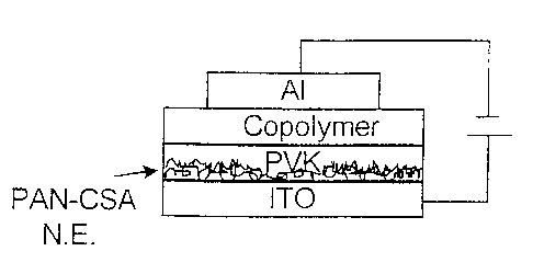
Figure 2 shows a schematic structure of a bilayer device with conducting
polyaniline
network electrode in accordance with one embodiment of the present invention.
Figure 3 shows a normalized optical absorption (dashed line) and PL of the
strapped
copolymer film (solid line), EL of a single layer device (solid line with
dots), and PL of
solution in xylenes (dotted line).
Figure 4 shows a comparison of (a) light-voltage and (b) Iight-current
characteristics
for a single layer device (square), a bilayer device (circle}, and a bilayer
device with PAN-
CSA network (triangle). Inset: EL spectra for the single layer device (dashed
line), the bilayer
device (solid line), and the bilayer device with network electrode (dotted
line).
Figure S shows a film PL of the pure wrapped copolymer and its blends with
PMMA
in various ratios with an excitation energy of 2.65 eV, and solution PL of the
copolymer in
xylenes. Inset: Film PL of a 1:20 blend with different excitation energies as
indicated in the
graph. Spectra are offset for clarity.
Figure 6 shows a schematic structure of an inverted light-emitting devices
with PPy as
emitting layer and PVK as hole transporting layer.
6
SU~STtf!!TE SHEEN' RULE 26)
CA 02262925 1999-02-O1
WO 98/06122 PCT/US97l134I0
Detailed Description of the Preferred Embodiments
In accordance with the foregoing summary of the invention, the following
presents a
detailed description of the preferred embodiment of the invention which is
presently
considered to be its best mode.
The synthesis of the pyridine-containing polymers has been reported earlier [9-
10]. For
single layer devices, the emitting layer was spin-cast from solutions in
formic acid (for PPy
and PPyV) or xylenes (for copolymers) (with a concentration ~10 mg/ml) onto
pre-cleaned
patterned ITO substrates with sheet resistance of ~15 S2/square at 1000-2000
rpm. For bilayer
devices, PVK layer was spin coated onto ITO substrate from solution in
tetrahydrofuran
(THF) (~10 mg/ml) at 3000 rpm. The emitting layer was then spin coated on top
of the PVK
layer from appropriate solutions. The conducting polyaniline network electrode
was formed
by a spin-cast blend of camphor sulfonic acid doped polyaniline (PAN-CSA) and
low
molecular weight host polymer poly(methyl methacrylate) (PMMA) (from Aldrich
Chemical
Co.) in an appropriate ratio in m-cresol. The host polymer PMMA was
subsequently washed
1 S away by xylenes. The PVK and emitting layers were similarly coated as in
the bilayer device.
All solutions were filtered using Gelman Acrodisc CR PTFE 1 pm filters. The
top metal
electrode was deposited by vacuum evaporation at a pressure below 10-6 ton. To
prevent
damage to the polymers, the substrate was mounted on a cold-water cooled
surface during
evaporation. Figure 2 shows schematically the structure of a bilayer device
with PAN-CSA
network electrode.
Absorption spectra were measured on spin-cast films using a Perkin-Elmer
Lambda 19
W/VIS/NIR spectrometer. Photoluminescence (PL) and EL were measured using a
PTI
fluorometer (model QM-1). The current-voltage (I-V) characteristics were
measured
7
SUBSItIUrE SHEEP (RULE 26j
CA 02262925 1999-02-O1
WO 98/06122 PCT/US97/13410
simultaneously with EL using two Keithley 195A multimeters while do voltage
was applied
by a HP 6218A DC power supply.
Figure 3 shows the optical absorption and PL of the strapped copolymer film
and EL
of a single layer device. For comparison, the PL of the strapped copolymer
solution in xylenes
is also shown. The film PL peaks at 2.05 eV with a shoulder at 2.25 eV As
compared to the
film absorbance, the peak of the film PL is redshifted 0.55 eV, which is
attributed to the
aggregates formed in the film [12]. The shoulder is suggested to come from the
unaggregated
site, and is supported by the PL measurements of blends in PMMA (see below).
It is noted
that although the strapped and the corresponding unstrapped copolymer show
similar features
in solution PL, no shoulder is found in the film PL for the unstrapped
copolymer, indicating
that the strapped side chains partially break the aggregates formation in the
film. The reversed
oscillator strength of the EL as compared to PL suggesting that the EL come
mainly from
unaggregated sites, although there is also a significant contribution from the
aggregate
emission.
Figure 4 compares the light-voltage (L-V) and EL-current {EL-I)
characteristics for a
single layer device, a bilayer device, and a bilayer device with PAN-CSA
network electrode
using the strapped copolymer as emitting layer. As compared to those of the
single layer
device, the quantum efficiency and brightness of the bilayer device increase
more than two
orders of magnitude, reaching ~0.3% and 300 cd/m2 respectively. PVK is a well
known hole
transporting/electron blocking polymer. Besides the function of enhance the
transport of holes
injected from anode, it blocks the transport of electrons injected from
cathode such that the
electrons accumulate at the PVK/copolymer interface. This greatly enhance the
probability of
radiative recombination. In addition, the PVK layer separates the
recombination zone from the
8
SUBSTIiUiE SHEET (RULE 26)
CA 02262925 1999-02-O1
WO 98/06122 PCTIUS9'~113410
metal electrode so that the radiative recombination is protected against the
well known non-
radiative quenching at the metal/polymer interfaces.
One side effect of using the PVK layer is that it increases the device
operating voltage
substantially. One effective way to reduce the device turn on voltage is to
use high surface
network electrode [13]. The concept behind the network electrode is that a
rough electrode
will create a non-uniform high electric field that enhances the charge
injection. This technique
has been successfully applied to PPV based devices [13]. By applying this
technique to the
PVK layer, the device operating voltage decreased significantly. For the
devices shown here,
the device operating voltage reduced from ~20 V to ~8 V (see Figure 4 (a)).
Since the
incorporation of the PAN-CSA network electrode does not modify the
PVK/copolymer
interface, the high quantum efficiency and brightness of the bilayer device
are maintained (see
Figure 4 (b)). Thus, the incorporation of the network electrode to the bilayer
device improves
the power efficiency dramatically. The species that is responsible for the
light generation in
the bilayer device is attributed partially to exciplexes formed at the
PVK/copolymer interface
and is identified by the PL measurements [14]. Figure 4 (b) inset compares the
EL spectra of a
single and a bilayer device using the strapped copolymer as emitting layer. As
compare to that
of the single layer device, the peak of the bilayer device, which comes from
the exciplex
emission at the PVK/copolymer interface, is blue-shifted 0.15 eV. A shoulder
in the bilayer
EL at the peak of the single layer EL suggests that the strapped copolymer EL
itself also
contribute to the bilayer EL.
The large difference between the film and solution PL of the pyridine-based
polymers
opens up an opportunity for fabricating voltage-controlled color-variable
light-emitting
devices. The aggregates formed in the polymer films result in significantly
red-shifted
luminescence as compared to isolated chains in solution. One expects to reduce
the red-shift
9
SIIBS1ITU1E SHEET (RULE 26j
CA 02262925 1999-02-O1
WO 98/06122 PCT/LTS97/.13410
of PL by breaking the aggregates formation. One effective way to break the
aggregation is to
blend the emissive polymer with an insulating host polymer, such as in PMMA.
Figure 5
shows the PL spectra of the pure wrapped copolymer and its blends with PMMA in
various
ratios. For comparison, the PL spectrum of the wrapped copolymer in solution
is also shown.
When the concentration of the emissive polymer decreases, the PL of the blends
gradually
blue shifted towards the solution PL, indicating partial break of the
aggregation of polymer
chains. Thus by choosing appropriate blend ratio, the emission color can be
controlled.
Furthermore, the PL spectra of the blends exhibit excitation energy
dependence, as shown in
Figure 5 inset for a blend with 1:20 (copolymer:PMMA) ratio excited at
different energies. As
the excitation energy increases, the PL strength of the higher energy peak
grows. In contrast,
no excitation energy dependence is found in pure copolymer PL. The excitation
energy
dependence of the blend PL make it possible to fabricate voltage controlled
mufti-color light-
emitting devices, and the work is in progress.
The high electron affinity of the pyridine-based polymers enables other novel
device
1 S configurations such as inverted light-emitting devices that are capable of
eliminating the use
of low workfunction metals. Polyp-pyridine) (PPy) has an electron affinity of
~3.5 eV [16J,
which allows metals with relatively high workfunction as electron injecting
contact. In the
inverted light-emitting devices with PPy as emissive layer, ITO and Au are
used as electron
and hole injecting contacts, respectively. The inverted (-)ITO/PPy/Au(+)
device show
improved device performance including quantum efficiency, brightness,
operating stability
and storage lifetimes as compared to the usual (+)ITO/PPy/Al(-) device. By
inserting a PVK
layer in between the PPy and Au, the device performance improves further
Figure 6 shows
schematically the device structure of the inverted light-emitting device with
PVK.
10
SU~;~UTE SNEET (RULE 26)
CA 02262925 2001-08-08
Conclusion
In summary, pyridine containing conjugated polymers and copolymers are
excellent
candidates for polymer light-emitting devices. The high electron affinity of
pyridine based
polymers enables the use of relatively stable metals such as A1 or even ITO as
efficient
electron injecting contacts. Taking advantages of the better electron
transport properties of
the pyridine-containing polymers, we fabricate bilayer devices utilizing PVK
as hole
transporting/electron blocking polymer. The bilayer device structure improves
the device
quantum efficiency and brightness significantly due to the charge confinement
and the
exciplex emission at the PVKlemitting polymer interface. The incorporation of
the
conducting polyaniline network electrode to PVK reduces the device turn on
voltage
significantly while maintaining the high efficiency and brightness of the
bilayer device. The
control of the aggregation in the~, polymer films by blending with insulating
host polymers
opens up the possibility of making voltage-controlled mufti-color light-
emitting devices.
T~ P TPYPH /~ P C
[1] J.H. Burroughes, D.D.C. Bradley, A.R. Brown, R.N. Marks, K. Mackay, R.H.
Friend,
P.L. Burns, and A.B. Holrnes, Nature 347, 539 (1990).
[2] D.D.C. Bradley, Synth. Met. 54, 401 (1993).
[3] J. Kido, Trends in Polymer Science 2, 350 (1994).
[4] D. Braun and A.J. Heeger, Appl. Phys. Lett. 58, 1982 (1991).
[5] N.C. Greenham, S.C. Morattl, D.D.C. Bradley, R.H. Friend, and A.B. Holmes,
Nature 365, 628 (1993).
[6] D.D. Gebler, Y.Z. Wang, .1.W. Blatchford, S.W. Jessen, L.B. Lin, T.L.
Gustafson,
H.L. Wang, T.M. Swager, A.G. MacDiarmid, and A.J. Epstein, J. Appl. Phys. 78,
4264 (1995).
[7] Y.Z. Wang, D.D. Gebler, L.B. Lin, J.W. Blatchford, S.W. Jessen, H.L. Wang,
and
A.J. Epstein, Appl. Phys. I~ett. 68, 894 (1996).
[8] J.W. Blatchford, Ph.D thcais, The Ohio State University (1996).
[9] T. Tamamoto, T. ITO, and K. Kubota, Chem. Lett, 153 (1988).
[10] M.J. Marsella, D.-K.Fu, and T.M. Swager, Adv. Mater. 7, 145 (1995).
[11]
[12] J.W. Blatchford, S.W. Jessen, L.-B. Lin, 'T.L. Gustafson, A.J. Epstein,
D.-K Fu, H.-
L. Wang, T.M. Swager, and A.G. MacDiarmid, Phys. Rev. B, in press; J.W.
CA 02262925 2001-08-08
Blatchford, T.L. Gustafson, A.J. Epstein, D.A. Vanden Bout, J. Kerimo,
D.A. Higgins, P.F. Barbara, D.K. Fu, T.M. Swager, and A.G. MacDiarmid, Phys.
Rev. B, in press.
[13] Y. Yang, E. Westerweele, C. Zhang, P. Smith, and A.J. Heeger, J. Appl.
Phys. 77,
694 (1995).
[14] D.D. Gebler, Y.Z. Wang, J.W. Blatchford, S.W. Jessen, T.L. Gustafson, D.-
K. Fu,
T.M. Swager, A.G. MacDiarmid, and A.J. Epstein, this proceedings.
[ls]
[ 16] T. Miyamae, D. Yoshimura, H. Ishii, Y. Uuchi, K. Seki, T. Miyazaki, T.
Koike, and
T. Yamamoto, J. Chem. lPhys. 103, 2738 (1995).
In view of the present disclosure or through practice of the present
invention, it will
be within the ability of one of ordinary skill to make modifications to the
present invention,
such as through the use of equivalent arrangements and compositions, in order
to practice the
invention without departing from the spirit of the invention as reflected in
the appended
claims.
12