Note : Les descriptions sont présentées dans la langue officielle dans laquelle elles ont été soumises.
CA 02265425 1999-03-12
TITLE OF THE INVENTION
Active Tunable Inductor
NAME OF INVENTOR
s Curtis Leifso and James W. Haslett
FIELD OF THE INVENTION
This invention relates to tunable active inductors, particularly active
inductors made
using a monolithic radio frequency integrated circuit (RFIC).
BACKGROUND OF THE INVENTION
A significant restraint in RF and microwave IC design stems from the
difficulty in
realizing an integrated passive inductor with sufficiently high Q over a broad
bandwidth. Large
space requirements, low inductance values and low Q factors make these
inductors unsuitable
1 s for precision applications.
Active designs have allowed larger inductance values to be realized. However,
the
active inductors published to date are limited in that they are often not
tunable. When
inductance tuning is introduced, the Q factor usually shows a strong
dependence on both the
tuning parameter and the frequency of operation. As a result, tuning both the
inductance and
2 o the Q factor requires an iterative tuning procedure.
A Q-enhancing technique has been described by Tokumitsu et al in [ 1 ]. In
this design a
cascode FET arrangement with resistive feedback is used such that when the
FETs are
matched, the active inductor's loss resistance can be canceled. The resistive
feedback
described in [ 1 ] was replaced with a common gate FET in [2] which offered
improved Q
2 s factor. everHow, tuning of Q of the inductance was not easily
accomplished.
Alinikula et al [3] described an alternative topology to that given in [2]
which ofr'ered
greater tuning flexibility. With this technique the effect of finite channel
conductance, gas , was
examined and a design was proposed which minimized sensitivity to gas. Using a
FET
operating in its linear region as a variable resistor, the frequency at which
maximum Q
CA 02265425 1999-03-12
2
occurred could be controlled. For narrow bandwidths the Q factor approached
500, however,
the loss resistance showed a strong frequency dependence.
A resonator design described by Haigh [4] introduced tuning of both the
resonant
frequency and the Q factor. A resonant circuit was formed by using two
integrators terminated
s in a capacitance and connected in a feedback loop. Although the resonant
frequency remained
independent of Q tuning, the circuit showed a large loss resistance for
frequencies below the
resonant frequency.
Tuning control of both inductance and Q factor was also reported in a topology
proposed by Lucyszyn and Robertson [S]. This design simulated an inductance
that was
1 o adjustable over a narrow range of values by changing the gate bias voltage
of a single FET.
The Q factor could also be tuned to be maximum at an arbitrary frequency.
However, as with
the previous design, the loss resistance showed an appreciable frequency
dependence resulting
in very narrow band performance.
A more recent design presented by Yong-Ho et al [6] expanded on a common Q
1 s enhancement technique using a single FET with lossy inductive feedback.
Instead of using a
passive feedback inductor, an active inductor circuit was used in this design.
The inductance
was made tunable over a wide range by varying the loss resistance of the
active feedback
circuit. Tuning of the Q factor was accomplished by varying the positive
supply voltage for all
FETs and could only be set to infinity for a narrow band of frequencies. The
loss resistance
2 o also varied over a wide range for frequencies outside of this narrow band.
List of References
1. T. Tokumitsu, T. Tanaka, M. Aikawa, S. Hara, Broadband Monolithic Microwave
Active
Inductor And its Application to Miniaturized Wide-band Amplifiers, in IEEE
Trans.
Microwave Theory Tech., vol 36, pp. 1920-1924, Dec 1988.
2 s 2. T. Tokumitsu, M. Aikawa, S. Hara, Lossless, Broadband Monolithic
Microwave Active
Inductors, in IEEE MTT-S Symp. Dig., 1989, pp. 955-958
3. P. Alinikula, R. Kaunisto, K. Stadius, Q-Enhancing Technique for High Speed
Active
Inductors, in 1994 IEEE International Symposium on Circuits and Systems, pp.
735-738.
4. D. G. Haigh, GaAs MESFET Active Resonant Circuit for Microwave Filter
Applications,
so in IEEE Trans. Microwave Theory Tech., vol 42, pp. 1419-1422, Jul 1994.
CA 02265425 1999-03-12
3
5. S. Lucyszyn, LD. Robertson, Monolithic Narrow-Band Filter Using Ultrahigh-Q
Tunable
Active Inductors, in IEEE Trans. Microwave Theory Tech., vol 42, No. 12, pp.
2617-2622,
Dec 1994.
6. C. Yong - Ho, H. Song-Cheol, K. Young-Se, A Novel Active Inductor and Its
Application
s to Inductance-Controlled Oscillator, in IEEE Trans. Microwave Theory Tech.,
vol 45, No. 8,
pp. 1208- 1213, Aug 1997.
SUNINIARY OF THE INVENTION
In this patent document, a novel design for an active inductor is presented
with more
Zo flexible tuning control than the prior art just described. It is an object
of the invention to
provide a series loss resistance of the simulated inductance that is frequency
independent over
a wide bandwidth. This constant resistance can be varied over a broad range of
both positive
and negative values with negligible impact on the effective inductance of the
circuit. The
inductance realized by the circuit is also tunable and remains independent of
series loss tuning.
15 Thus, an active inductor is provided preferably implemented as a fully
integrated GaAs
MESFET active inductor.
Both the inductance and loss resistance are tunable with the inductance
independent of
series loss tuning. DC tuning of the loss resistance can also be achieved with
complete
independence of the loss resistance and inductance.
2 o Bandwidth of the active inductor may be selected according to the
fabrication
technology employed and the intended application of the circuit.
According to an aspect of the invention, there is thus provided an active
inductor
formed as a monolithic integrated circuit. The active inductor has an input
impedance that
simulates an inductance with a loss resistance. The active inductor comprises
a first capacitor
2 s and a second capacitor connected at a common voltage point V2, and each of
the first
capacitor and second capacitor being ungrounded. Circuit elements are arranged
about the
capacitors to provide voltage differentials across the capacitors, the voltage
differentials being
selected so that the loss resistance of the active inductor is tunable
independently of the
inductance of the active inductor. The circuit elements are preferably
controlled sources, and
so the controlled sources are preferably implemented as MESFETs.
CA 02265425 1999-03-12
4
According to a further aspect of the invention, a negative impedance circuit
is provided
in parallel with the input of the active inductor. This increases the
bandwidth of the active
inductor.
These and other aspects of the invention are described in the detailed
description of the
s invention and claimed in the claims that follow.
BRIEF DESCRIPTION OF THE DRAWINGS
There will now be described preferred embodiments of the invention, with
reference to
the drawings, by way of illustration only and not with the intention of
limiting the scope of the
1 o invention, in which like numerals denote like elements and in which:
Fig. 1 shows a controlled source schematic of a first embodiment of an active
inductor
according to the invention;
Fig. 2 is a circuit showing a realization of the first embodiment using
MESFETs;
Fig. 3 is a graph showing measured effect of varying the Q tuning capacitor C2
in Figs.
1 s 1 and 2;
Fig. 4 is a graph showing measured, simulated and theoretical effective loss
resistance
tuning range as a function of C2 in Figs. 1 and 2;
Fig. S is a graph showing simulated and measured effect of varying the
inductance
tuning capacitor C1 in Figs. 1 and 2;
2o Fig. 6 is a graph showing measured, simulated and theoretical :inductance
tuning range
as a function of C1 in Figs. 1 and 2;
Fig. 7 is a schematic showing bandwidth limiting FET parasitic capacitors in
the
embodiment of Figs. 1 and 2;
Fig. 8 is a controlled source schematic of a second embodiment of the
invention;
2 s Fig. 9 is an implementation of the embodiment of Fig. 8 using MOSFETs;
Fig. 10 is a schematic showing a third embodiment of the invention in which
gate bias is
used to tune inductance and loss resistance;
Fig. 11 is a graph showing the measured and simulated effect of varying the
inductance
tuning voltage Vg~ in Figs. 1 and 2;
CA 02265425 1999-03-12
Fig. 12 is a graph showing the measured effect of varying the loss resistance
tuning
voltage Vgl in Figs. 1 and 2;
Fig. 13 is a controlled source schematic of a negative impedance circuit for
use with the
invention; and
s Fig. 14 is a realization of the embodiment of Fig. 13 using MESFETs.
DETAILED DESCRIPTION OF PREFERRED EMBODIMENTS
In this patent document, "comprising" means "including", and does not exclude
other
elements being present. In addition, a reference to an element by the
indefinite article "a" does
1 o not exclude the possibility that more than one of that element is present.
A capacitor is any
device that provides capacitance in a circuit.
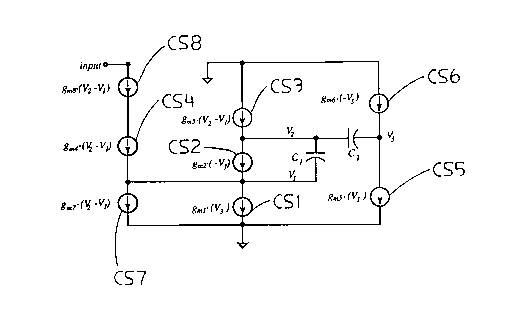
Fig. 1 shows a controlled source format of an embodiment of a circuit for
carrying out
the invention. The controlled sources CS1-CS8 can be realized with a variety
of transistors or
other circuits, ie. MOS, bipolar, etc. The active inductor shown in Fig. 1 is
preferably formed
is as a monolithic integrated circuit. The controlled sources are preferably
MESFETs as shown in
Fig. 2. The active inductor shown in Figs. 1 and 2 has an input impedance that
simulates an
inductance with a loss resistance. As shown in Figs. 1 and 2, a capacitor C,
and a capacitor C2
are connected at a common voltage point V2. Capacitor C1 is separated from
ground by a
controlled source CS1, and capacitor C2 is separated from ground by a
controlled source CSS.
2o Circuit elements formed of controlled sources CS1-CS8 (equivalent to
MESFETs Ml-M8 in
Fig. 2) are arranged about the capacitors C1 and CZ to provide voltage
differentials across the
capacitors C, and CZ such that the loss resistance is tunable independently of
the inductance of
the active inductor. The circuit elements include a first controlled source
CS1 (implemented
with MESFET Ml in Fig. 2) connected between capacitor C1 and ground, and a
second
25 controlled source CS2 (implemented with MESFET M2 in Fig. 2) connected
across the
capacitor C1 between the first controlled source CS1 (drain of M7) and the
common voltage
point V2. Controlled sources CSI-CS3 implemented as MESFETs M1, M2 and M3 are
connected in a common source cascode arrangement. The drain of MESFET M3 is
connected
to Vdd, and the common voltage point VZ is connected between controlled source
CS3 (source
30 of M3) and controlled source CS2 (drain of M2). Plural controlled sources
CSS and CS6
CA 02265425 1999-03-12
6
(implemented with M5, M6 and M9 in Fig. 2) are arranged as an inverting
feedback loop such
that the voltage Vl between the capacitor C1 and the first controlled source
CS1 has the same
poles as V2. An input stage including controlled sources CSB, CS4 and CS7 is
arranged to set
the input impedance proportional to the difference between V1 and V2. Currents
are arranged
to flow through the controlled sources according to the values placed next to
them in Fig. 1,
where g""~ represents the transconductance of controlled source x. In the case
of the MESFETs
of Fig. 2, current flow is controlled by controlling the gate voltages.
From Fig. 1, the input impedance Z;n can be found from straightforward nodal
analysis.
Small signal analysis of the circuit gives V,, V2 and V3 as
-gm3Yin (ClgmS gm2C2 +J~ C1C2)
(A + jc~B)
V2 -gm3~n (C~gmS +gm2C2 +.~~ ClC2)
(A + j~B)
-Om3Vn ( ~lam5 +Om2C2 +J~ ClC2)
(A + jr.~B)
where A=C,C2(g-m2 + gn,3 -~' 2gn5~
B-C2 ~gm22 + gm2gm3/ + CI ~gmSgm3 + grn5gm2/
assuming that C, and C2 are much larger than the parasitic capacitances of
each FET,
preferably at least 10 times as large. Both V, and Tr2 are first order
functions of the input port
voltage, V;n .
The feedback voltage V3 causes Vl and VZ to differ only by a sign inverted
term in their
2 o numerator terms. By subtracting Vl from Vz only a single constant term
remains in the
numerator expressions. Setting the small signal input current equal to gm4(!~2-
Yl~ , the
simulated inductance of the circuit, Ls;m, is given by
Lsim = CI gm2 + gm3 + 2gm5
Zgm2g'm3gm4
CA 02265425 1999-03-12
7
which is independent of C2 and tunable via Cl, with a series loss resistance
given by
gm2 + $m2g'm3 KCl gm3 - gm2
Rloss = + gm5
Zgm2gm3gm4 C2 Zgm2gm3gm4
which is frequency independent and tunable via C2 .
K is a curve fitting constant where 0.3 < K < 0.4. For an appropriate choice
of FET
dimensions, Rloss can be made tunable over a wide range of both positive and
negative
resistances. Since the simulated inductance is independent of C2, the
simulated inductance is
independent of series loss resistance tuning.
to Similar characteristics can be obtained by using (V3 -VZ), etc. Various
realizations of
the circuit are possible. One example of a realization is shown in Fig. 2.
Both the simulated
inductance, Ls;m , and the series loss resistance, Ross are made tunable with
two variable
capacitors C1 and C2 . If Rioss is to be tunable independently of the
inductance, the input
impedance expression must be of the form
Z~ =~UJL(C1)+Iyoss (C1,C2)
which consists of an inductance, and a frequency independent series resistance
that are some
function of the tuning capacitors Cj and C2. Rloss is determined by the
capacitive ratio CllC2
and the inductance is set by the absolute value of capacitance C, or C2. The
input impedance
will depend only on C, and C2 provided they are much larger than the FET
parasitic
2 o capacitances, preferably at least 10 times as large. This allows the two
capacitors CI and C2
shown in Fig. 1 to be used for separate tuning of LS;", and Rloss
respectively.
In Fig. 2, MESFETs Ml, M2, and M3 are connected in a common source cascode
topology, with the gate of M3 connected to V;", and the gate of M2 grounded.
MESFETS M5,
M6 and M9 are also connected in a common source cascode topology, and likewise
MESFETs
2 5 M,, M4 and M8, which form the input stage. M8 has its gate grounded, while
the gate of M9 is
connected to the common voltage point between the capacitors Cl and C2. The
gate of MS is
connected between M, and M2. The common voltage point V2 is also connected to
the gates of
CA 02265425 1999-03-12
8
M4 and M8. The gate of M, is connected to V4 between the source of MS and the
drain of M9.
The sources of M,, MS and M, are all grounded.
With MESFETs Ml , M2 and M3 in a common source cascode topology as shown in
Fig. 2, two voltages V, and Y2 are generated such that if the current into the
input port, i", , is
s set proportional to V2 - VI both LS;", and Rloss will depend on CI and Cz.
Independence of the inductance from Ross can only be achieved provided Ls;m
does not
depend on both C, and CZ . This is accomplished with the second cascode
arrangement
consisting of MS , M6 and M, used to form an inverting feedback loop. The
inverting feedback
loop sets the gate voltage of Mj to Vj, which is a phase shifted version of VI
resulting in V~ and
1 o V2 to have the same poles.
The input stage formed by M, , MQ and M8 forms a voltage to current conversion
that
sets the input impedance Z;" proportional to V2 - VI . M4 sets the small
signal input current
equal to g,"4(Vz - Vl) resulting in an input impedance with resistive and
inductive terms only
and with the required form given in the equation for input impedance. FET M9
has no effect
1 s on the feedback voltage V3 and is only required to set the gate voltage of
M, to V4 = gma(Va -
Vi), provided M, and M4 are matched. If M, and M4 are matched, then the
voltage to current
conversion given by M,, MQ and M8 has no impact on node voltages VI or V2
since MQ injects a
current into node V, equal to that pulled from the node by M,.
FETs M, and M8 are included to reduce the sensitivity of Z;" to the high
channel
2 o conductance of the input stage FETs. Alternative stacked FET arrangements
can be used to
minimize the effects of gdsa and gas8 . However, the proposed topology reduces
the number of
FETs required as well as minimizes the effects ofM4's capacitive parasitics.
In an actual realization of the embodiment of the invention shown in Fig. 2, a
I,um
GaAs MESFET process was used resulting in a total chip area of l.2mm x l.7mm
for the
2 s complete circuit. The test chip was wire bonded to a chip Garner and the
input impedance
measurements were done with an HP8510C Network analyzer interfaced through an
Elite Test
jig.
In order to test the fabricated design, both the inductance and Q tuning
capacitors were
built as an array of MIM (metal-insulator-metal) capacitors each 30% of the
nominal value
CA 02265425 1999-03-12
9
required for infinite Q. By connecting these smaller capacitors in parallel,
the initial
capacitances of CI and C2 were each made 30% larger than required. When tuning
the input
impedance each capacitor was reduced by small increments by progressively
breaking air
bridges supporting the second metal layer between each sub-capacitor,
effectively removing it
s from the parallel connection.
With CI fixed to give a constant inductance, C2 was lowered in small
decrements
resulting in the set of impedance plots shown in Fig. 3. Initially C2 was
larger than required for
infinite Q causing the first impedance measured to have a large positive loss
resistance (+1552)
as predicted by the equation for series loss resistance. Decreasing C2
increased the Q factor,
1 o until sufficiently large Q was realized as shown in Fig. 3 .
Continuing to lower C2 beyond this point makes the series loss resistance
negative in
accordance with the equation for series loss resistance. The wide loss
resistance tuning range
is shown in Fig. 4 in comparison to the expected values from both simulation
and the equation
for series loss resistance. Rloss can be tuned over a 2552 range of both
positive and negative
15 resistances corresponding to a 9.3 pF change in C2.
The measured series loss resistance is a nearly linear fi~nction of the tuning
capacitor
C2. This linearity is maintained for negative series resistances when C2 is
further decreased
below 10 pF. Below 9 pF the assumption that Cz is much larger than the sum of
parasitic
capacitances is no longer valid and Rloss predicted by the equation for series
loss resistance
2 o begins to diverge from measured and simulation results shown in Fig. 4.
Fig. 5 shows the effects of the parameter K in the equation for series loss
resistance.
This parameter allows the effects of the large FET channel conductances to be
modeled
without complicating the expression.
Tuning of the inductance is accomplished by varying Cl. As C, was varied, the
ratio
25 C,lCa was held constant. This ensures that Rloss stays constant in
accordance with the
equations for simulated inductance and series loss resistance since R~oSS is
determined by the
ratio C,lC2.
Different inductance values were measured and plotted to give the set of
curves shown
in Fig. 5. The good agreement between the simulations and the measurements was
obtained by
CA 02265425 1999-03-12
adjusting the DC gate bias slightly to account for a wide variation in the
saturated drain current
of the FETs between test chips. The effective bandwidth of each inductance was
not affected
by tuning of either CI or C2. The measured inductance tuning range is shown in
Fig. 6 with
expected values from simulation and the equation for simulated inductance. As
in the case of
s loss resistance tuning, the inductance dependence on CI is also
approximately a linear function.
Fig. 6 also shows the expected Ls;m when the maximum drain current for a given
FET
geometry, Idss, is 5% below the nominal value for the process. As shown, the
dynamic tuning
range of Ls;m is not altered by variations in lass . The wider dynamic range
measured can be
reflected in the simulations by changing the DC bias conditions in the
simulations. The smaller
1 o tuning range given by the equation for simulated inductance is a result of
neglecting the large
channel conductance of the FETs. As shown in Fig. 4 and Fig. 6 the equations
for simulated
inductance and series loss resistance are reasonably accurate given their
simplicity and proved
useful throughout the design of the circuit. Simulation results show that a
method of
electronic tuning can be easily introduced without compromising tuning range
by replacing
both CI and C2 with varactor diodes. Since neither capacitor is grounded, each
varactor diode
must be placed in series with a fixed capacitance for DC blocking.
In conclusion, for the embodiment of Fig. 2, measurement results confirm the
tuning
control of both the inductance and loss resistance and the independence of the
inductance from
loss resistance tuning. Simple analytical expressions have been presented for
both the
2 o inductance and the series loss resistance. Analytic predictions and
simulations were found to
be in good agreement with measured results. Electronic tuning of both the
inductance and loss
resistance can be achieved with varactor diodes or gate voltage tuning.
A second active inductor according to the invention is shown in Figs. 8 and 9.
Fig. 8
shows a controlled source format, while Fig. 9 shows a realization. Controlled
sources CSl,
2s CS2, CS3 and CS4 in Fig. 8 are connected in a common source cascode
arrangement, with the
source of CS1 and the drain of CS3 both grounded, and with input voltage
provided between
CS4 and CS2. Capacitors C, and C2 are connected to a common voltage point V2
between
CS3 and CS4. Capacitor C1 is placed across the controlled sources CS2 and CS4,
while
capacitor CZ is isolated from ground by controlled source CSS, and capacitor
C1 by CSI.
CA 02265425 1999-03-12
11
When the currents are set through the controlled sources as shown in Fig. 9,
the input
impedance is given by
~ C2 ~m2 + gm4 + gm5 ~ + 1 + 1 CZ - 1
m
gm3gm4gm5 gm4 gm3 CI
In this case, the inductance is tunable using C2, and the loss resistance is
independently tunable
using C,.
In the realization given in Fig. 9, MOSFETs M1, M2, M3 and M4 correspond to
to controlled sources CS1, CS2, CS3 and CS4 respectfully. MOSFET MS
corresponds to
controlled source CSS. MOSFETs M7 and M8 are provided to set the gate voltage
of
MOSFETs M1 and M2 to achieve the controlled sources specified in Fig. 8. The
gate of
MOSFET M8 is grounded, and the gates of MOSFETs M3 and M4 are tied to the
voltage
point V3, which is connected to the drain of MOSFET M5.
15 Fig. 1 is an ideal representation. If drain-source output conductances are
taken into
account (ie if voltage-sensitive resistors are placed across each controlled
source in the
diagram), then it is possible to get a lossy inductor where the inductance and
loss resistance
can be independently varied by adjusting two bias voltages in the circuit. The
range of
adjustment is significantly better in this case (a factor of two larger) and
the inductance and
2 0 loss resistance can be tuned completely independently of each other.
Adjustment of bias
voltages has advantages over use of variable capacitors. The active inductor
using adjustment
of bias voltages is shown in Fig. 10. Measured results for the MESFET
realization in Fig. 10
are shown in Figs. 11 and 12.
The embodiment of the invention shown in Fig. 10 has the same general form as
Fig. 1
2s and Fig. 2. Capacitors C1 and CZ are connected in the same way to the
cascode as the
capacitors C1 and C2 in Figs. 1 and 2. The gate of M~ is provided with an
adjustable bias
voltage through resistance Rc, and variable voltage VG~. The gate of Ml is
provided with an
adjustable bias voltage through resistance Rm and variable voltage VG1. Tuning
of inductance
CA 02265425 1999-03-12
12
is achieved by varying the bias voltage VG, on the gate of MESFET M~. Tuning
of loss
resistance is achieved by varying the bias voltage VGl on the gate of MESFET
Ml.
Each MESFET has an output conductance that can be varied by varying that
transistor's do gate voltage. For MESFETs, the output conductance can be made
quite
sensitive to the do gate voltage by operating at small bias currents. The
output conductance
can also be made to be quite insensitive to do gate voltage by operating at
large bias currents,
which is useful for capacitive tuning.
Analysis, simulation and measurement results have shown that the active
inductor
equivalent circuit of Figs. 1 and 2 is an inductor in parallel with a fixed
low loss capacitance for
1 o frequencies approaching 10 GHz. It is this small capacitance that limits
the resonant frequency
of the active inductor to 1.1 GHz. Simulations show that the circuit behaves
as an ideal
inductor when this capacitance is removed or significantly reduced. According
to simulation
experiments, this range can be increased to 3.3 GHz by placing a negative
impedance converter
in parallel with the input to the inductor. The negative impedance converter
is shown in Figs.
13 and 14.
Analysis and simulation results confirm that it is the capacitive parasitics
of FETs M3
and M8 that collectively appear as an equivalent capacitance, Ceg , to ground
as shown in Fig.
7. Casa , Cgd3 and CgdB shown in Fig. 7 are negligible in comparison to Cgs3
and thus C gs3
dominates the high frequency performance of the circuit. The active inductor's
input
2 o impedance can be arranged to have very low sensitivities to the remaining
FET parasitics
including large channel conductance and other FET capacitances. The erect of
Ceg can be
reduced in several ways to considerably extend the effective bandwidth of the
inductor. Since
a channel length of l,um was used for all FETs in the MESFET embodiment shown
in Fig. 2,
the gate width required for a reasonable transconductance was also large,
resulting in gate-to-
source capacitances of the order of 0.6 pF. Simulation results show that a
submicron process
with a gate length less than O.S,um increases the inductor's effective
bandwidth as a result of
significantly lower gate-to-source capacitances. Alternatively, a negative
impedance converter
or NIC at the input port may be used. The tunable negative capacitance with
sufficiently low
conductive loss provides useful independent tuning of the parallel capacitance
or complete
CA 02265425 1999-03-12
13
removal if desired. If the inductor is used in applications requiring an LC
resonator, Ceg is
desirable and can be left alone without any consequence to circuit
performance.
Referring to Fig. 13, an exemplary negative impedance converter is shown,
which is
provided connected in parallel to the input of the circuit shown in Fig. 1.
The negative
s impedance converter is formed from a series connected controlled source CSI,
a complex
impedance Z1, a controlled source CS3, a second complex impedance Z2 and a
third
controlled source CS2. The controlled sources are arranged to have the
currents specified in
the figure. A realization is shown in Fig. 14. MESFETs M1, M2 and M3 are the
controlled
sources CSI, CS2 and CS3. The voltage at the gate of M2 is set by V;". The
voltage at the
1 o gate of M 1 is set by the voltage between the drain of M3 and impedance
Z2. The voltage at the
gate of M3 is set to ground. The operation of the negative impedance converter
is conventional
in itself, but the arrangement provides improved bandwidth when used in
association with the
active tunable inductor described here. The input impedance of the NIC is
given by
Zrn=- 1a + 1 + 1 +Z,-Zz
Om2 gm3 gm4
1 s The capacitors C 1 and C2 in Fig. 1 may be implemented as enhanced FET
parasitics, but
this implementation is not preferred. In addition, C1 and C2 could be
implemented by
transistors. It is believed that the bandwidth of the active tunable inductor
is limited only by
available electronics, and ranges from 1 MHz to over 3 GHz.
Immaterial modifications may be made to the invention described here without
2 o departing from the essence of the invention.