Sélection de la langue

Search

Sommaire du brevet 2266322 

Énoncé de désistement de responsabilité concernant l'information provenant de tiers

Une partie des informations de ce site Web a été fournie par des sources externes. Le gouvernement du Canada n'assume aucune responsabilité concernant la précision, l'actualité ou la fiabilité des informations fournies par les sources externes. Les utilisateurs qui désirent employer cette information devraient consulter directement la source des informations. Le contenu fourni par les sources externes n'est pas assujetti aux exigences sur les langues officielles, la protection des renseignements personnels et l'accessibilité.

Disponibilité de l'Abrégé et des Revendications

L'apparition de différences dans le texte et l'image des Revendications et de l'Abrégé dépend du moment auquel le document est publié. Les textes des Revendications et de l'Abrégé sont affichés :

  • lorsque la demande peut être examinée par le public;
  • lorsque le brevet est émis (délivrance).
(12) Brevet: (11) CA 2266322
(54) Titre français: CIRCUIT DE PROTECTION CONTRE LES COURANTS HAUTE INTENSITE POUR UNE INTERFACE TELEPHONIQUE
(54) Titre anglais: HIGH CURRENT PROTECTION CIRCUIT FOR TELEPHONE INTERFACE
Statut: Périmé et au-delà du délai pour l’annulation
Données bibliographiques
(51) Classification internationale des brevets (CIB):
  • H02H 09/02 (2006.01)
  • H02H 03/02 (2006.01)
  • H02H 03/087 (2006.01)
  • H04M 01/74 (2006.01)
(72) Inventeurs :
  • WONG, WAYNE KWOK-WAI (Etats-Unis d'Amérique)
  • RODRIGUEZ, SAUL (Etats-Unis d'Amérique)
(73) Titulaires :
  • FLUKE CORPORATION
(71) Demandeurs :
  • FLUKE CORPORATION (Etats-Unis d'Amérique)
(74) Agent: OYEN WIGGS GREEN & MUTALA LLP
(74) Co-agent:
(45) Délivré: 2011-10-25
(22) Date de dépôt: 1999-03-23
(41) Mise à la disponibilité du public: 1999-10-03
Requête d'examen: 2004-12-15
Licence disponible: S.O.
Cédé au domaine public: S.O.
(25) Langue des documents déposés: Anglais

Traité de coopération en matière de brevets (PCT): Non

(30) Données de priorité de la demande:
Numéro de la demande Pays / territoire Date
09/054,922 (Etats-Unis d'Amérique) 1998-04-03

Abrégés

Abrégé français

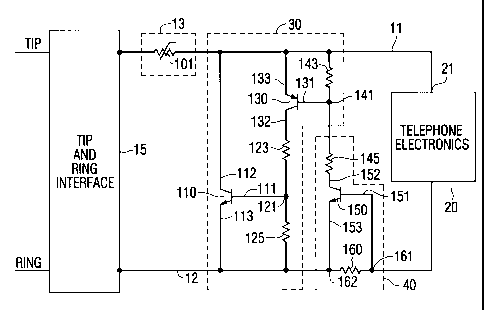
Trousse de contrôle de téléphone protégé contre les courants à haute intensité par un circuit de protection qui maintient une circulation du courant en ligne pour le fonctionnement continu de la circuiterie fonctionnelle de l'appareil téléphonique. Un élément limiteur de courant en série installé dans l'acheminement du courant en ligne, entre une interface des conducteurs de tête et de nuque et la circuiterie de la trousse de contrôle de téléphone. Un circuit shunt de courant est disposé entre les lumières des interfaces des conducteurs de tête et de nuque du circuit protégé, en aval de l'élément limiteur de courant. Un circuit détecteur de courant surveille le courant en boucle et commande le fonctionnement du circuit shunt. Si une surintensité de courant survient pendant une période prolongée, la dissipation d'énergie résultante, de concert avec le courant élevé, provoque le passage de l'élément limiteur de courant à un état d'impédance élevé. Lorsque la surintensité de courant est terminée, l'élément en série retourne à un état de basse impédance.


Abrégé anglais

A telephone test set protected from an excessive current condition by a protection circuit that maintains sufficient loop current flow for continuous operation of the telephone equipment's functional circuitry. A series current-limiting element installed in the loop current path between a tip and ring interface and the circuitry of the telephone test set. A current shunting circuit installed across the tip - ring ports of the protected circuit downstream of the current-limiting element. A current sense circuit monitors the loop current and controls the operation of the shunting circuit. If a substantial overcurrent condition persists for an extended period of time, the resulting power dissipation associated with the high current flow will cause the current limiting element to change to a high impedance state. Once the overcurrent condition terminates, the series element will revert to its low impedance state.

Revendications

Note : Les revendications sont présentées dans la langue officielle dans laquelle elles ont été soumises.


WHAT IS CLAIMED IS:
1. A protection circuit for protecting an output circuit from a source of
electrical energy, the protection circuit comprising:
input terminals arranged to be coupled to said source of electrical
energy;
output terminals arranged to be coupled to said output circuit;
a variable impedance device coupled in a current flow path between
said input and output terminals, and through which all current
flowing into said input terminals from said source of electrical
energy flows irrespective of the impedance state of said variable
impedance device;
an overcurrent bypass circuit coupled to receive said all current flowing
through said variable impedance device and being operative to
controllably cause a portion of said all current flowing through
said variable impedance device to be diverted around said output
circuit to be protected through a bypass path away from said
output circuit; and
a current flow sense circuit coupled to monitor current flow through a
current flow path through said output circuit and being operative,
in response to an overcurrent condition, to cause said overcurrent
bypass circuit to controllably divert a first portion of said all
current flowing through said variable impedance device to be
directed through said bypass path away from said output circuit,
while allowing a second portion of said all current flowing
through said variable impedance device, and sufficient to operate
said output circuit, to continue to flow through said current flow
path and said output circuit.
2. A protection circuit according to claim 1, wherein said variable imped-
ance device is operative, in response to said overcurrent condition
7

reaching a prescribed level, to change from a low impedance state to a
high impedance state, thereby reducing current flow therethrough to a
value sufficient to continue to operate said output circuit, but less than
a value that could damage said overcurrent by-pass circuit.
3. A protection circuit according to claim 2, wherein said variable imped-
ance device is operative, in response to said overcurrent condition
dropping below said prescribed level, to change from said high imped-
ance state to said low impedance state.
4. A protection circuit according to claim 1, wherein said output circuit
comprises a telephone circuit and said input terminals are arranged to
be coupled with tip and ring conductors of a telephone line.
5. A protection circuit according to claim 4, wherein said variable imped-
ance device comprises a series current-limiting element installed in a
loop current flow path between a tip and ring interface and circuitry of
telephone equipment to be protected.
6. A protection circuit according to claim 5, wherein said overcurrent
by-pass circuit is installed across tip--ring ports of said circuitry of
telephone equipment to be protected downstream of said series cur-
rent-limiting element.
7. A protection circuit according to claim 1, wherein said overcurrent
by-pass circuit includes a current input-output path of a controlled
switching device, which is controlled by said current flow sense circuit.
8. A protection circuit according to claim 1, wherein said current flow
sense circuit includes a current sensing resistor installed in said current
flow path, and a threshold circuit which is coupled to monitor voltage
8

across said current sensing resistor and to control the operation of said
overcurrent by-pass circuit.
9. A protection circuit according to claim 8, wherein said overcurrent
by-pass circuit includes a current input-output path of a controlled
switching device, which is controlled by said threshold circuit.
10. A method of protecting a signaling circuit from an overcurrent condi-
tion in a current supply path for said signaling circuit, while allowing
said signaling circuit to continue to operate in the presence of said
overcurrent condition comprising the steps of:
(a) monitoring current flow through a variable impedance device,
which is installed in said current supply path and through which
all current supplied from a source of electrical energy for operat-
ing said signaling circuit flows irrespective of the impedance
state of said variable impedance device; and
(b) in response to said overcurrent condition in said current supply
path, diverting a first portion of said all current flowing though
said variable impedance device away from said signaling circuit,
while allowing a second portion of said all current flowing
through said variable impedance device, that is sufficient to
operate said signaling circuit, to continue to flow through said
signaling circuit.
11. A method according to claim 10, wherein said signaling circuit com-
prises a telephone circuit and wherein said current supply path is
coupled with tip and ring conductors of a telephone line.
12. A method according to claim 10, further including the step of:
(c) in response to said overcurrent condition reaching a prescribed
level, placing said variable impedance device in a high imped-
9

ance state, thereby reducing current flow therethrough to a value
sufficient to continue to operate said signaling circuit.
13. A method according to claim 12, wherein step (b) includes diverting
said first portion of current through a current shunting circuit that
by-passes said signaling circuit.
14. A method according to claim 12, wherein step (c) comprises placing
said variable impedance device in a high impedance state that reduces
current flow therethrough to a value sufficient to continue to operate
said signaling circuit, but less than a value that could damage said
current shunting circuit.
15. A method according to claim 14, wherein said variable impedance
device comprises a series current-limiting element installed in a loop
current flow path between a telephone tip and ring interface and said
signaling circuit.
16. A method according to claim 14, further including the step of:
(d) in response to said overcurrent condition dropping below said
prescribed level, placing said variable impedance device in a low
impedance state.
17. An overcurrent protection circuit for protecting a signaling circuit from
an overcurrent condition comprising:
a variable impedance installed in a current flow path through which all
current is supplied from a source of electrical energy to said
signaling circuit, irrespective of the impedance state of said
variable impedance, and having a relatively low impedance state
in response to said all current flowing therethrough being less
than a threshold, and having a relatively high impedance state in

response to said all current flowing therethrough being equal to
or greater than said threshold; and
a current by-pass circuit coupled between said variable impedance and
said signaling circuit and being operative, in response to said all
current flowing through said variable impedance and said current
flow path for said signaling circuit being greater than an
overcurrent threshold, to selectively by-pass a first portion of
said all current flowing through said variable impedance around
said signaling circuit, while allowing a second portion of said all
current flowing through said variable impedance to continue to
flow through said current flow path for said signaling circuit.
18. An overcurrent protection circuit according to claim 17, wherein said
signaling circuit comprises a telephone circuit, and wherein said
current flow path is adapted to be coupled to tip and ring conductors of
a telephone line.
11

Description

Note : Les descriptions sont présentées dans la langue officielle dans laquelle elles ont été soumises.


CA 02266322 1999-03-23
H6623, DR180
HIGH CURRENT PROTECTION CIRCUIT FOR TELEPHONE INTERFACE
The present invention relates to communication systems, and in particular is
directed
to a circuit for protecting the electronic circuitry of telephone equipment,
from an excessive
current condition such as may occur, if the telephone ring and tip leads
become directly coupled
to a low impedance path to a high voltage source, such as battery or loop feed
circuit.
The fact that manufacturers of telephone equipment provide instruction manuals
and
guidelines for use and maintenance of their equipment is no guarantee that
users will not
subject such equipment to potentially damaging operational and/ or
environmental conditions.
Indeed, it is often the case that telephone repair technicians connect their
portable test set
io equipment to very high voltage and current sources, such as power supplies
or telephone loop
feed circuits having very low series resistances and/or high voltages. When
this happens, loop
currents considerably in excess of the rated value (e.g., on the order of 100 -
150 ma) may result.
Prolonged operation of the equipment in such a high current condition will
eventually lead to
failure of the equipment's electronic circuitry.
is One proposal to deal with the high current condition has been to switchably
interrupt
or insert a high impedance device in the loop current path to the protected
circuitry. While this
overcurrent intervention approach prevents damage to the circuit to be
protected, it also
effectively renders the telephone equipment inoperative until the high current
condition has
terminated.
20 The present invention includes a protection circuit comprising input
terminals arranged
to be coupled to a source of electrical energy, output terminals arranged to
be coupled to an
output circuit to be protected, a variable impedance device coupled in a
current flow path of
said output circuit between said input and output terminals, an overcurrent by-
pass circuit
coupled to divert current from said current flow, characterized by a current
flow sense circuit
2s coupled to monitor current flow through said current flow path and being
operative, in
response to an overcurrent condition, to cause said overcurrent by-pass
circuit to controllably
divert a portion of current away from said current flow path through said
output circuit, while
allowing current sufficient to operate said output circuit to continue to flow
through said
current flow path and said output circuit.
30 The invention also includes a method of protecting a signaling circuit from
an
overcurrent condition in a current supply path for said signaling circuit,
while allowing said
signaling circuit to continue to operate in the presence of said overcurrent
condition comprising
1

CA 02266322 1999-03-23
H6623, DR180
the steps of:
(a) monitoring current flow through said current supply path; (b) in response
to
said overcurrent condition in said current supply path, diverting a portion of
current away from
said current supply path, while causing current sufficient to operate said
signaling circuit to
s continue to flow through said current supply path and said signaling
circuit.
Rather than effectively shutting down the telephone equipment until the
overcurrent
condition subsides, the invention employs selectively controlled high current
protection circuit
that is effective to maintain sufficient current flow for continuous operation
of the telephone
equipment's functional circuitry, while at the same time controllably by-
passing excess and/or
io reducing the amount of loop current being drawn into the equipment, that
could potentially
damage the protected circuitry.
Conveniently, the over current protection circuit comprises a series current-
limiting
element installed in the loop current flow path between a tip and ring
interface (bridge rectifier)
and the circuitry of the telephone equipment to be protected. An overcurrent
current shunting
is or by-pass circuit is installed across the tip - ring ports of the
protected circuit downstream of
the current-limiting element. This overcurrent by-pass circuit may include the
collector-emitter
path of a bipolar transistor, the base of which is coupled through a level-
shifting and amplifier
transistor to a current sense circuit.
The current sense circuit may include a current sensing bipolar transistor,
which is
20 controllably turned on by the voltage across a relatively low value current
sense resistor
installed in the loop current path through the telephone's electronic
circuitry to be protected.
By relatively low value resistance is meant one that does not affect the
operational performance
of the circuitry to be protected.
During normal operation, the current flow through the current sense resistor
will be less
25 than that sufficient to forward bias the current sense transistor, so that
the shunting circuitry is
turned off, and all of the loop current flows through the tip - ring path,
including the series
current-limiting element, the protected circuitry and the current sense
resistor. If the tip - ring
terminals of the telephone (test) set are coupled to a high current source,
such as being placed
directly across the terminals of battery, then the current flow through the
current sense resistor
30 will increase to a value sufficient to turn on the current sense
transistor. This, in turn will cause
the overcurrent by-pass transistor to divert or by-pass a portion of the
current that would
otherwise flow through the electronic circuitry by way of the tip - ring loop
current path.
For a medium magnitude overcurrent condition (e.g., on the order of 100 - 150
ma), this
by-pass operation is sufficient to allow useful loop current (e.g., on the
order of 20 - 100 ma) to
2

CA 02266322 1999-03-23
H6623, DR180
flow through the protected circuitry, while allowing the excess current to be
diverted without
damaging the current-shunting components. However, if a substantial
overcurrent condition
persists for an extended period of time, the resulting power dissipation
associated with this high
current flow will cause the series high impedance element to change from its
low impedance
state to its high impedance state. In this high impedance state, sufficient
operational loop
current (e.g., 20 - 30 ma) will continue to flow through the protected
circuitry, yet the
components of the shunting circuitry will be protected. Once the overcurrent
condition
terminates, the series element will revert to its low impedance state.
Advantageously, a selectively controlled high current protection circuit that
is effective
io to provide sufficient current flow for maintaining operation of the
telephone equipment's
functional circuitry, while controllably by-passing excess and/or reducing the
amount of loop
current being drawn into the equipment, that could potentially damage the
protected circuitry.
The invention will now be described, by way of example, with reference to the
accompanying drawings in which:
is Figure 1 is a functional block diagram of a high current protection circuit
in accordance
with the present invention; and
Figure 2 is a schematic diagram of the high current protection circuit of
Figure 1.
Figure 1 illustrates the over current protection circuit; and Figure 2 is a
circuit schematic
of Figure 1. The over current protection circuit is shown in dotted lines 10,
comprises a series
20 current-limiting element 13 installed in the loop current flow path 11-12
between a tip and ring
interface (bridge rectifier) 15 and circuitry 20 of the telephone equipment to
be protected. An
overcurrent current shunting or by-pass circuit 30 is installed across the tip
- ring ports 21 - 22
of the protected circuit 20 downstream of the current-limiting element 13.
Figure 2 shows the
overcurrent by-pass circuit 30 that includes the collector-emitter path of a
bipolar transistor,
25 coupled through a level-shifting and amplifier transistor to a current
sense circuit 40.
The current sense circuit 40 is coupled in the loop current path and is
operative to
monitor the magnitude of the loop current flowing therethrough. During normal
current
operation, wherein the loop current is less than a prescribed threshold (e.g.,
on the order of one
hundred milliamps), the output of the current sense circuit 40 will maintain
the overcurrent by-
30 pass circuit 30 in a non-shunting state. However, in the event of an
overcurrent condition, such
as would occur if the tip - ring terminals of the telephone equipment were
directly coupled to
a high current source, such as being placed directly across the terminals of
power supply
(battery), the current sense circuit 40 will detect the increased current flow
and trigger the
overcurrent-shunting operation of the overcurrent by-pass circuit 30. For a
medium magnitude
3

CA 02266322 1999-03-23
H6623, DR180
overcurrent condition (e.g., 100 - 150 ma), loop current in excess of that
necessary to provide
useful loop current (e.g., on the order of 20 - 100 ma) to the telephone
circuitry is shunted
through by-pass circuit 30, while still allowing useful current to be supplied
to and operate the
telephone circuitry 20.
s If the overcurrent condition is substantial, however, the resulting power
dissipation
associated with this high current flow will cause the series current-limiting
element 13 to change
from its low impedance state to a high impedance state, thereby substantially
reducing the
magnitude of the loop current (e.g., to a value flow on the order of 20 - 30
ma). During this high
impedance state, this small but sufficient operational loop current will
continue to flow through
io the circuitry 20, so that the telephone circuitry remains operational. In
response to termination
of the overcurrent condition, the series element will revert to its low
impedance state.
Figure 2 shows a example of a circuit schematic for implementing the
functional block
diagram of Figure 1 comprising a resettable fuse element 101 (such as a
standard conductive
polymer-based power dissipation device) as the current-limiting series element
13 installed in
is the tip path 11 between the tip and ring interface (bridge rectifier) 15
and the first end 21 of the
telephone circuitry 20 to be protected. The current shunt circuit 30 is shown
as including an
overcurrent by-pass or shunting NPN bipolar transistor 110 having its
collector-emitter path
112-113 coupled in circuit between the fuse element 101 and the ring path 12.
The base 111 of overcurrent by-pass transistor 110 is coupled to a common node
20 connection 121 of a pair of resistors 123 and 125, which are coupled in
series with the collector-
emitter path 132-133 of a level shifting and amplifier PNP bipolar transistor
130, between the
tip path-installed fuse element 101 and the ring path 12. The base 131 of PNP
bipolar transistor
130 is coupled to a common connection 141 of a pair of resistors 143 and 145.
Resistors 143 and 145 are coupled in series with the current sense circuit 40,
which
25 includes the collector-emitter path 152-153 of a current sensing NPN
bipolar transistor 150,
coupled between the tip path 11 and the ring path 12. The base 151 of current
sense transistor
150 is coupled to a first end 161 of a current sense resistor 160, a second
end 163 of which is
coupled to the emitter 153 of current sense transistor 150. The current sense
resistor 160, which
is coupled in the loop current path between the ring lead 12 and a second end
21 of the
30 telephone's electronic circuitry 20 to be protected, has a relatively low
resistance (e.g., on the
order of four to six ohms) so that it does not affect the operational
performance of the circuitry
20.
During normal (non-overcurrent) operation, the current flow through current
sense
resistor 160 will be less than that sufficient to forward bias the base-
emitter junction of current
4

CA 02266322 1999-03-23
H6623, DR180
sense transistor 150, so that each of transistors 110, 130 and 150 is turned
off, and all of the loop
current flows through the tip - ring path, including the tip path-installed
fuse element 101, the
circuitry 20 and the current sense resistor 160. (As noted above, the
magnitude of the current
sense resistor 160 is sufficiently low that it does not affect the operational
performance of the
s circuitry 20.)
If the tip - ring terminals of the telephone (test) set are coupled to a high
current source,
such as being placed directly across the terminals of battery as a non-
limiting example, then the
current flow through the current sense resistor 160 will increase to a value
sufficient to forward
bias the base-emitter junction of and turn on the current sense transistor
150. The resulting
io current flow through resistors 143 and 145 and the collector-emitter path
152-153 of current
sense transistor 150 will forward bias the base-emitter junction of level
shift transistor 130,
which turns on transistor 130 and causes current flow through resistors 123
and 125. This in turn
forward biases the overcurrent by-pass transistor 110, causing its collector-
emitter path 112-113
to divert a portion of the current that would otherwise flow through the
electronic circuitry 20
15 by way of the tip - ring loop current path.
For a medium magnitude overcurrent condition (e.g., on the order of 100 - 150
ma), the
above-described operation is sufficient to allow useful loop current (e.g., on
the order of 20 -100
ma) to flow through the circuitry 20, on the one hand, while allowing
excessive current to be
diverted without damaging the diverting or shunting components. However, if
the overcurrent
20 condition is substantial (e.g., it exceeds a few hundred milliamps for an
extended period of
time), then the resulting power dissipation associated with this high current
flow will cause the
resettable fuse element 101 to change from its low impedance state to a high
impedance state.
During this high impedance state of the current-limiting element 101,
sufficient operational loop
current (e.g., 20 - 30 ma) will continue to flow through the circuitry 20;
however, the
2s components of the shunting circuitry 30 will be protected. Once the
overcurrent condition
terminates, the series element 101 will revert to its low impedance state, as
described above.
In this state, the telephone circuitry and the protection circuit of the
invention appear
as a continuous load on the telephone line, as seen from upstream central
office switching
equipment. Since (a small amount of) loop current continues to flow, the
central office
3o equipment does not detect that the telephone circuit has gone on-hook and
drop the call. The
invention also accommodates the situation where the user attempts to go off-
hook during a
ringing signal, which may have peaks on the order of well in excess of 100
volts. In a
conventional protection circuit, transitioning to its high impedance
protection state may prevent
the ring-trip circuit at the central office from responding, so that the
ringing signal does not

CA 02266322 1999-03-23
H6623, DR1SO
immediately terminate, as the normally low off-hook termination resistance
will not be sensed.
This constitutes an annoyance to the user, who is not accustomed to the phone
ringing when
it is off-hook.
Thus, rather than switchably interrupt or insert a high impedance device in
the loop
s current path to the circuitry to be protected, which effectively renders the
telephone equipment
inoperative until the high current condition has terminated, the overcurrent
protection
mechanism of the present invention maintains sufficient current flow for
continuous operation
of the telephone equipment's functional circuitry, while at the same time
controllably by-passing
excess and/ or reducing the amount of loop current being drawn into the
equipment, that could
io potentially damage the protected circuitry.
A telephone test set protected from an excessive current condition by a
protection circuit
that maintains sufficient loop current flow for continuous operation of the
telephone
equipment's functional circuitry. A series current-limiting element installed
in the loop current
path between a tip and ring interface and the circuitry of the telephone test
set. A current
is shunting circuit installed across the tip - ring ports of the protected
circuit downstream of the
current limiting element. A current sense circuit monitors the loop current
and controls the
operation of the shunting circuit. If a substantial overcurrent condition
persists for an extended
period of time, the resulting power dissipation associated with the high
current flow will cause
the current limiting element to change to a high impedance state. Once the
overcurrent
2 0 condition terminates, the series element will revert to its low impedance
state.

Dessin représentatif
Une figure unique qui représente un dessin illustrant l'invention.
États administratifs

2024-08-01 : Dans le cadre de la transition vers les Brevets de nouvelle génération (BNG), la base de données sur les brevets canadiens (BDBC) contient désormais un Historique d'événement plus détaillé, qui reproduit le Journal des événements de notre nouvelle solution interne.

Veuillez noter que les événements débutant par « Inactive : » se réfèrent à des événements qui ne sont plus utilisés dans notre nouvelle solution interne.

Pour une meilleure compréhension de l'état de la demande ou brevet qui figure sur cette page, la rubrique Mise en garde , et les descriptions de Brevet , Historique d'événement , Taxes périodiques et Historique des paiements devraient être consultées.

Historique d'événement

Description Date
Le délai pour l'annulation est expiré 2014-03-25
Lettre envoyée 2013-03-25
Accordé par délivrance 2011-10-25
Inactive : Page couverture publiée 2011-10-24
Préoctroi 2011-07-28
Inactive : Taxe finale reçue 2011-07-28
Un avis d'acceptation est envoyé 2011-02-09
Lettre envoyée 2011-02-09
Un avis d'acceptation est envoyé 2011-02-09
Inactive : Approuvée aux fins d'acceptation (AFA) 2011-01-31
Requête pour le changement d'adresse ou de mode de correspondance reçue 2011-01-21
Requête pour le changement d'adresse ou de mode de correspondance reçue 2010-11-29
Requête pour le changement d'adresse ou de mode de correspondance reçue 2010-11-05
Modification reçue - modification volontaire 2010-02-26
Inactive : Dem. de l'examinateur par.30(2) Règles 2009-09-03
Inactive : CIB de MCD 2006-03-12
Inactive : Correspondance - Transfert 2005-01-12
Lettre envoyée 2005-01-10
Exigences relatives à la nomination d'un agent - jugée conforme 2005-01-10
Exigences relatives à la révocation de la nomination d'un agent - jugée conforme 2005-01-10
Lettre envoyée 2005-01-10
Inactive : Lettre officielle 2005-01-10
Inactive : Demande ad hoc documentée 2005-01-07
Inactive : Lettre officielle 2005-01-07
Exigences pour une requête d'examen - jugée conforme 2004-12-15
Requête en rétablissement reçue 2004-12-15
Toutes les exigences pour l'examen - jugée conforme 2004-12-15
Exigences de rétablissement - réputé conforme pour tous les motifs d'abandon 2004-12-15
Lettre envoyée 2004-12-14
Demande visant la nomination d'un agent 2004-11-17
Demande visant la révocation de la nomination d'un agent 2004-11-17
Inactive : Abandon.-RE+surtaxe impayées-Corr envoyée 2004-03-23
Inactive : Page couverture publiée 1999-10-03
Demande publiée (accessible au public) 1999-10-03
Lettre envoyée 1999-06-17
Inactive : Correspondance - Formalités 1999-05-12
Inactive : Transfert individuel 1999-05-11
Inactive : CIB en 1re position 1999-05-11
Inactive : Certificat de dépôt - Sans RE (Anglais) 1999-04-28
Demande reçue - nationale ordinaire 1999-04-23

Historique d'abandonnement

Date d'abandonnement Raison Date de rétablissement
2004-12-15

Taxes périodiques

Le dernier paiement a été reçu le 2011-03-02

Avis : Si le paiement en totalité n'a pas été reçu au plus tard à la date indiquée, une taxe supplémentaire peut être imposée, soit une des taxes suivantes :

  • taxe de rétablissement ;
  • taxe pour paiement en souffrance ; ou
  • taxe additionnelle pour le renversement d'une péremption réputée.

Les taxes sur les brevets sont ajustées au 1er janvier de chaque année. Les montants ci-dessus sont les montants actuels s'ils sont reçus au plus tard le 31 décembre de l'année en cours.
Veuillez vous référer à la page web des taxes sur les brevets de l'OPIC pour voir tous les montants actuels des taxes.

Historique des taxes

Type de taxes Anniversaire Échéance Date payée
Taxe pour le dépôt - générale 1999-03-23
Enregistrement d'un document 1999-05-11
TM (demande, 2e anniv.) - générale 02 2001-03-23 2001-01-09
TM (demande, 3e anniv.) - générale 03 2002-03-25 2002-02-18
TM (demande, 4e anniv.) - générale 04 2003-03-24 2003-02-21
TM (demande, 5e anniv.) - générale 05 2004-03-23 2004-02-16
Enregistrement d'un document 2004-11-15
2004-12-15
Requête d'examen - générale 2004-12-15
TM (demande, 6e anniv.) - générale 06 2005-03-23 2005-03-16
TM (demande, 7e anniv.) - générale 07 2006-03-23 2006-03-03
TM (demande, 8e anniv.) - générale 08 2007-03-23 2007-03-02
TM (demande, 9e anniv.) - générale 09 2008-03-25 2008-03-03
TM (demande, 10e anniv.) - générale 10 2009-03-23 2009-03-03
TM (demande, 11e anniv.) - générale 11 2010-03-23 2010-03-02
TM (demande, 12e anniv.) - générale 12 2011-03-23 2011-03-02
Taxe finale - générale 2011-07-28
TM (brevet, 13e anniv.) - générale 2012-03-23 2012-02-29
Titulaires au dossier

Les titulaires actuels et antérieures au dossier sont affichés en ordre alphabétique.

Titulaires actuels au dossier
FLUKE CORPORATION
Titulaires antérieures au dossier
SAUL RODRIGUEZ
WAYNE KWOK-WAI WONG
Les propriétaires antérieurs qui ne figurent pas dans la liste des « Propriétaires au dossier » apparaîtront dans d'autres documents au dossier.
Documents

Pour visionner les fichiers sélectionnés, entrer le code reCAPTCHA :


Pour visualiser une image, cliquer sur un lien dans la colonne description du document. Pour télécharger l'image (les images), cliquer l'une ou plusieurs cases à cocher dans la première colonne et ensuite cliquer sur le bouton "Télécharger sélection en format PDF (archive Zip)" ou le bouton "Télécharger sélection (en un fichier PDF fusionné)".

Liste des documents de brevet publiés et non publiés sur la BDBC .

Si vous avez des difficultés à accéder au contenu, veuillez communiquer avec le Centre de services à la clientèle au 1-866-997-1936, ou envoyer un courriel au Centre de service à la clientèle de l'OPIC.


Description du
Document 
Date
(aaaa-mm-jj) 
Nombre de pages   Taille de l'image (Ko) 
Dessin représentatif 1999-09-26 1 8
Abrégé 1999-03-22 1 23
Revendications 1999-03-22 3 155
Dessins 1999-03-22 1 20
Revendications 1999-05-11 5 153
Revendications 2010-02-25 5 210
Description 1999-03-22 6 376
Dessin représentatif 2011-09-18 1 10
Certificat de dépôt (anglais) 1999-04-27 1 165
Courtoisie - Certificat d'enregistrement (document(s) connexe(s)) 1999-06-16 1 116
Rappel de taxe de maintien due 2000-11-26 1 112
Rappel - requête d'examen 2003-11-24 1 123
Courtoisie - Lettre d'abandon (requête d'examen) 2004-05-31 1 167
Accusé de réception de la requête d'examen 2005-01-09 1 176
Avis de retablissement 2005-01-09 1 170
Avis du commissaire - Demande jugée acceptable 2011-02-08 1 162
Avis concernant la taxe de maintien 2013-05-05 1 171
Correspondance 1999-05-03 1 23
Correspondance 1999-05-11 6 183
Correspondance 2004-11-16 2 67
Correspondance 2004-12-13 1 17
Correspondance 2005-01-06 1 15
Correspondance 2005-01-06 1 21
Correspondance 2005-01-09 1 14
Correspondance 2005-01-09 1 18
Taxes 2005-03-15 1 31
Correspondance 2010-11-04 1 31
Correspondance 2010-11-28 1 28
Correspondance 2011-01-20 2 75
Correspondance 2011-07-27 1 34