Note : Les descriptions sont présentées dans la langue officielle dans laquelle elles ont été soumises.
CA 02266993 2001-06-22
-1-
STANDARD FOOTPRINT AND FORM FACTOR RJ-45 CONNECTOR WITH
INTEGRATED SIGNAL CONDITIONING FOR HIGH SPEED NETWORKS
1 . Field of the Invent i_on
The present invention relates to e_Lectronic jacks and
connectors, and more particularly to modular phone-style RJ-
45 Category-3 and Cate:~ory-5 network physical interface
connectors.
2. Description of the F?rior Art
Network interface connections have conventionally
included some form of ss.gnal conditioning near the RJ-45
Category-3 or Category-_'~ modular connector. The usual purpose
is to block spurious signals, e.g., high frequency noise,
differential-mode direct: current (DC), and common mode
voltages. Various magnet:ics assemblies from HALO Electronics
(Redwood City, CA) like 1=he ULTRATr' series of sixteen-pin SOIL
isolation modules are used to meet the requirements of IEEE
Standard 802.3 for 10/100BASE-TX and ATM155 applications. A
very informative background on connectors and their network
applications, and a lon<~ citation of prior art, is provided
by John Siemon, et al., in United States Patent 5,474,474,
issued December 12, 1995.
A few connector manufacturers have started to put some
signal conditioning cc:~m~~~~nents inside the bodies of their
connectors. for example, Peter Scheer, et al., describe a
connector jack assembly with a rear insert that includes
signal conditioning cc:~mponents, in United States Patent
5,647,767, issued Jul.~~ 15, 1997. f-:owever, the descriptions
show there is a rather large housing extension necessary in
the back of t:he connec:~tors to accc>mmodate a horizontally
oriented printed circi:it board. True footprint that results
CA 02266993 1999-03-25
-2-
would prohibit the embodiments of Peter Scheer, et al., from
being able to make a form, fit, and function substitution of
ordinary connectors already designed into various network
products. Venkat A. Raman also describes another connector
jack with an insert body having encapsulated signal
conditioning components, in United States Patent 5,587,884,
issued December 24, 1996. A common mode choke and other
magnetics are described as being encapsulated in the insert
molding. The Raman disclosure also describes a rather large
connector housing to accommodate a small horizontally
oriented printed circuit board for the magnetics in the rear.
So it too would not be able to directly substitute for many
of the standard connections being marketed.
Gregory Loudermilk, et al., recognized the need for a
filtered modular jack that provides the signal conditioning
needed by high speed communications systems, and that
'occupies approximately the same amount of board space on a
printed circuit motherboard as do current modular jacks".
But then their United States Patent, 5,687,233, issued
November 11, 1997, diagrams and describes a mounting pin
array with a large extension to the rear to accomanodate a
transmit and receiver printed circuit board in a rear
housing.
A very modest rearward extension to a RJ-11 modular jack
is described by Yukio Sakamoto, et al., in United States
Patent 5,069,641, issued December 3, 1991. A small printed
circuit board is shown vertically oriented directly above the
line of mounting pins and has a common mode choke coil
mounted to it. Gregory Loudermilk, et al., commented that
Yukio Sakamoto, et al., did not teach signal conditioning in
their RJ-11 connector that was sophisticated enough for high
speed applications like LAN and ATM switches.
. CA 02266993 1999-03-25
-3-
It is therefore an object of the present invention to
provide a modular connector with integrated signal
conditioning in a component package that has a compatible
footprint with prior art modular connectors that lack such
signal conditioning.'
It is a further object of the present invention to
provide a modular connector system in which a single-row
multi-port modular connector for printed circuit board
mounting may accept a second single-row multi-port modular
connector.
It is a still further object of the present invention to
provide a modular connector system that will reliably survive
motherboard solder operations during the assembly of other
components.
Briefly, a two-row, eight-port modular connector
embodiment of the present invention comprises a lower row
with a four-bay insulative housing that accepts four RJ-45
style jacks from its front, and a short-height gang of four
separate molded inserts from the opposite side. The four-bay
insulative housing and each molded insert are essentially the
same as a standalone four-port, single-row modular connector
so that the single-row modular connector can be quickly and
easily converted to the eight-port, two-row modular
connector. Such a conversion would include an upper row
four-bay insulative housing that also accepts four RJ-45
style jacks from its front and a tall gang of four molded
inserts that have forward extensions of their spring contacts
so they can reach from behind far enough forward over the
lower first row. A three-piece Faraday shield comprises a
lower middle part that covers the rear of each of the four
first-row lower-row molded inserts, an aft part that covers
the rear of each of the four upper-row molded inserts, and a
CA 02266993 2001-06-22
-4-
forward part that covert; the front and aides of both the
four-bay insulative hou~~ings and part o.f the top of the
housing. After assembly, t:he three Faraday shield pieces are
electrically connected ~so that they constitute a continuous
shield around the whole of the eight-port, two-row modular
connector. Each molded insert includes a signal conditioning
circuit that provides a proper electrical coupling between a
physical interface device (PHY) or encoder/decoder and an
unshielded twisted pair (UTP) cable to a high speed computer
network. The circuit connections for the integrated signal
conditioning in each i:n:~ert may be welded, rather than
soldered.
Accordingly, in one of its aspects, the present
invention provides an R~T--45 style modular connector,
comprising: a plastic :rectangular housing with an open front
end to receive a matching RJ-45 style modular jack, and an
opposite open back end; ~~ contact spring assembly of a
plurality of wires in separate circuits that pass forward
through said open back end into the back of said open front
end of the housing, wherein the contact spring assembly
includes a plastic blc;clc that supports the plurality of wires
by a right angle turn and is vertically oriented with respect
to the plurality of wires, and wherein the plastic block
inserts and locks intc~:~aid open back end of the housing; a
set of mounting pins is disposed at a bottom edge of said
plastic blo c: for conne~~tion to a printed motherboard; and a
signal conditioning part disposed i_n said plastic block for
providing signal cond~_tioning of signals passing from said
set of mounting Fins t:o said contact spring assembly;
wherein, sai<~ signal c::ondi_tioning part is fully disposed in
said vertica-_ly c>rient:.ed plastic block and directly over the
CA 02266993 2004-04-29
-4a-
set of mounting pins such that a rear extension compartment
that would otherwise be necessary is within a standard form
factor, and that further provides for multilevel stacking.
In a still further aspect, the present invention
provides an RJ-45 style modular connector, comprising: a
plastic rectangular housing with a first plurality of open
front end bays for each bay to receive a matching RJ-45 style
modular jack, and an opposite second plurality of open back
end bays; and wherein each pair of open front and back end
bays is associated with: a contact spring assembly of a
plurality of wires in separate circuits that pass forward
through said open back end into the back of said open front
end of the housing, wherein the contact spring assembly
includes a plastic block that supports the plurality of wires
by a right angle turn and is vertically oriented with respect
to the plurality of wires and wherein the plastic block
inserts and locks into said open back end of the housing; a
set of mounting pins in two fore-and-aft parallel rows on a
uniform pin spacing is disposed at a bottom edge of said
plastic block for connection to a printed motherboard; and a
signal conditioning part disposed in said plastic block for
providing signal conditioning of signals passing from said
set of mounting pins to said contact spring assembly;
wherein, said signal conditioning part is fully disposed in
said vertically oriented plastic block and directly over the
set of mounting pins such that a rear extension compartment
that would otherwise be necessary is within a standard form
factor, and that further provides for multilevel stacking.
In particular, in one preferred embodiment, the connector has
at least one of the signal conditioning parts including a
common choke to suppress noise interference associated with
CA 02266993 2004-04-29
-4b-
an Ethernet LAN operating on a LAN media cable connected with
a corresponding contact spring assembly. In another
preferred embodiment, the connector has at least one of the
signal conditioning parts including an isolation transformer
to block direct current signals associated with an Ethernet
LAN operating on a LAN media cable connected with a
corresponding contact spring assembly. In still another
preferred embodiment, the connector has at least one of the
signal conditioning parts including an impedance matching
transformer to couple Ethernet LAN signals between said set
of mounting pins connected with a LAN media cable.
An advantage of the present invention is that a multi-
port modular connector is provided that can be used to
retrofit ordinary modular connectors because the integrated
signal conditioning does not require a back extension to the
main housing.
Another advantage of the present invention is that a
multi-port modular connector is provided with integrated
signal conditioning that will not disconnect during soldering
operations of the motherboard.
These and other objects and advantages of the present
invention will no doubt become obvious to those of ordinary
skill in the art after having read the following detailed
description of the preferred embodiments which are
illustrated in the various drawing figures.
CA 02266993 1999-03-25
-5-
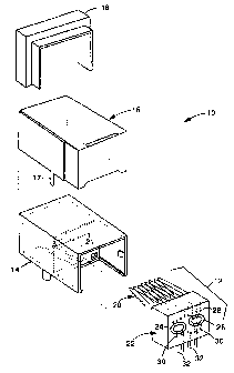
Fig. 1 is a perspective exploded assembly diagram of a
single-port modular connector embodiment of the present
invention;
Fig. 2 is a perspective exploded assembly diagram of a
four-port, single-row modular connector embodiment of the
present invention';
Fig. 3 is a perspective exploded assembly diagram of an
eight-port two-row modular connector embodiment of the
present invention;
Fig. 4 is a side view of the eight-port two-row modular
connector of Fig. 3 showing the critical maximum rear
extension "A" required to maintain plug compatibility with
preexisting connectors and showing the critical placement of
the signal conditioning circuitry directly above the
corresponding PCB mounting pins;
Fig. 5 is a side view of a three-row modular connector
that started with the two-row modular connector of Figs. 3
and 4. Fig. 5 shows the critical maximum rear extension "B"
required to maintain plug compatibility with preexisting
connectors. The signal conditioning circuitry is critically
placed directly above each successively deeper rows of PCB
mounting pins;
Fig. 6 is a schematic diagram of a DC blocking and
filter-capacitor circuit, as may be required in the coupling
of a PHY device to a cable medium in a 100BASE-T network
application, and that may be implemented within the
integrated signal conditioning part of any of the molded
inserts shown in Figs. 1-5;
Fig. 7 is a schematic diagram of a DC blocking and
series choke circuit, as may be required in the coupling of a
PHY device to a cable medium in a 100BASE-T network
application, and that may be implemented within the
CA 02266993 2001-06-22
-6-
integrated signal conditioning part of any of the molded
inserts shown in Figs. 7_--5; and
Fig. 8 is a schematic diagram of a common mode choke
circuit, as may be required in the coupling of a PHY device
to a cable medium in a 7_00BASE-T network application, and
that may be implemented within the integrated signal
conditioning part of any of the molded inserts shown in Figs.
1-5.
DETAILED DESCRIP7.'ION OF THE PREFERRED EMBODIMENT
Fig. 1 illustrates a single-port printed-circuit-board
(PCB) mount modular connector embodiment of the present
invention, referred to herein by the general reference
numeral 10. The modular connector 10 comprises a snap-in
insert assembly 12 that _installs :into a back end of a plastic
housing 14 and solders down to a PCB. A metal Faraday shield
16 covers the top, side: and back of the assembled insert 12
and housing 14 and provides for electromagnetic-radiation
(EMR) protection. A tab 17 is intended to be soldered to a
groundplane of the PCP.. A conductive flexible gasket 18 is
used to collar the front: end of the assembled housing 14 and
shield 16 and provide R,J-45 jack grounding by bridging the
small distance to an in;~talled jack. For further details of
this construcaion, seek Jnited States Patent 5,647,765,
issued July 1.5, 1997, t~~ Haas, et al.
A group of spring c_~.onnectors 20 passes through a hole 21
in a dividing wall within the housing 14 to ultimately
connect with any RJ-45 ~~l.ugged in from the front. The RJ-45
connection system is an industry standard and is ubiquitous
in the data network i.r~.dust:ry. The group of spring connectors
20 provides f=or eight industry defined circuit connections
that pass through a plastic insert. body 22.
CA 02266993 2001-06-22
The typical RJ-45 connection to a data network is part
of the physical interface layer and requires a modest amount
of signal conditioning. =Lt is critical to the present
invention that such signal conditioning be implemented
entirely within the volume of the insert body 22, and
especially net off-connector on the PCB or in a "dog-house"
back extension. The pin--out, pin placements, and overall form
factor of the modular connector 1.0 are critical because it
must be the form, fit, and function equivalent to preexisting
PCB's that were designed for prior art modular connectors.
The point of mounting the=_ signal conditioning inside the
insert body 22 is to save the PCB real estate that would
otherwise be needed or not available, and to gain the EMR-
related advantage of being inside the Faraday shield 16.
Such signal conditi~~ning is represented in Fig. 1 with
the example of a pair of torroid transformers 24 and 26,
e.g., as produced and marketed by HALO Electronics (Redwood
City, CA). Fc>r example, see, United States Patent 5,656,985,
issued August. 12, 199, to Peter Lu, et al.
Other e~:amples of :signal conditioning can include
ferrite slab: and cores, chip capacitors, and baluns. Such
signal conditioning i; ~~onnected by wires that are welded at
points 28 to the grou~> of spring connectors 20. The PCB side
of the signal conditic:~ning is attached by welding to points
2'. 30 on the tops of a sa:~t of eight PCB wiring posts 32. Such
welding is critical ta:~ the present. invention, as opposed to
soldering, because thcint:ended PC:B mount will be subjected
to soldering operatiorus, e.g., vapor phase or wave solder,
that could re-melt tha:>. signal conditioning connections and
cause a conductivity l:mpz-edict:ability. Some consumers of such
prior art modular conruector combat. this; problem by using
CA 02266993 1999-03-25
_g-
x-ray imaging to inspect the attachments after soldering
operations. The shields are then installed after passing the
x-ray inspection. The present invention is intended to make
such x-ray inspections unnecessary, and thereby reduce
manufacturing costs.
There are applicatiOris where soldering or using _
conductive epoxy could be used instead of welding the signal
conditioning components to the PCB wiring posts.
Fig. 2 illustrates a four-port, single-row modular
connector embodiment of the present invention, referred to
herein by the general reference numeral 40. The modular
connector 10 comprises a four-bay insulative housing 42 that
accepts RJ-45 style jacks from its front and a gang of four
molded inserts 44-47. Each such molded insert 44-47 is
essentially the same as that described for the snap-in insert
assembly 12 illustrated in Fig. 1. A two-piece Faraday
shield comprises an aft part 48 that covers the rear of each
of the four molded inserts 44-47, and a forward part 50 that
covers the front, top, and sides of the four-bay insulative
housing 42. Each bay of the four-bay insulative housing 42
is preferably the same so that a series of standardized
molded inserts 44-47 may be produced that offer a selection
of signal conditioning options for special applications.
Fig. 3 illustrates an eight-port, two-row modular
connector embodiment of the present invention, referred to
herein by the general reference numeral 60. The eight-port
modular connector 60 comprises a lower row with a four-bay
insulative housing 62 that accepts four RJ-45 style jacks
from its front and a gang of four molded inserts 64-67. The
four-bay insulative housing 62 and each molded insert 64-67
is essentially the same as that described for the four-port,
single-row modular connector 40 illustrated in Fig. 2. In
fact, the two are preferably identical so that the single-row
modular connector 40 of Fig. 2 can be quickly and easily
CA 02266993 1999-03-25
-9-
converted to the eight-port, two-row modular connector 60 of
Fig. 3.
Such conversion would include an upper row four-bay
insulative housing 68 that accepts four RJ-45 style jacks
from its front and a gang of four molded inserts 70-73 that
have forward extensions of their spring contacts so they can
reach from behind far enough over the lower first row.
A three-piece Faraday shield comprises a lower middle
part 74 that covers the rear of each of the four lower-row
molded inserts 64-67, an aft part 76 covers the rear of each
of the four upper-row molded inserts 70-73, and a forward
part 78 that covers the front and sides of the four-bay
insulative housings 62 and 68, and part of the top of housing
68. After assembly, the three Faraday shield pieces 74, 76,
and 78 are electrically connected so that they constitute a
continuous shield around the whole of the eight-port, two-row
modular connector 60. Each molded insert 64-67 and 70-73
includes a signal conditioning circuit that provides a proper
electrical coupling between a physical interface device (PHY)
or encoder/decoder and an unshielded twisted pair (UTP) cable
to a high speed computer network. In some applications, such
signal conditioning and the circuitry used to effect the
condition may have to vary in circuitry and component types
from insert to insert. In such cases the present invention
includes a snap-together construction that would allow a user
to mix-and-match inserts by their signal conditioning types
to their assigned positions in the bay rows.
Fig. 4 is a side view of the eight-port two-row modular
connector 60 of Fig. 3. A critical maximum rear extension
"A" is required to maintain plug compatibility with
preexisting connectors, dimension "A" is therefore limited to
0.100 inch. A first and second row of PCB mounting and
connection pins 80 and 81 actually comprise four pins each in
two rows for each molded insert 64-67. Similarly, a third
and fourth row of PCB mounting and connection pins 82 and 83
CA 02266993 1999-03-25
-10-
actually comprise four pins each in two rows for each molded
insert 70-73. Therefore, each molded insert 64-67 and 70-73
has eight pins that will be individually referred to herein
as P1-P8. Pins P1, P3, P5, and P7 are positioned on 0.100
inch centers in a row set forward of the other row of pins by
0.100 inch. The second row of pins comprises P2, P4, P6, and
P8, and they too are set on 0.100 inch centers but staggered
0.050 inch relative 'to pins P1, P3, P5, and P7. A post 84
helps secure and align the eight-port two-row modular
connector 60 to a PCB motherboard 86. A set of plated-
through holes 87-91 (in rows) respectively allow connections
to the post 86 and connection pin rows 80-83.
Fig. 4 further shows the critical placement of the
signal conditioning circuitry directly above the
corresponding PCB mounting pins. Additional circuitry can be
included in the free spaces above the molded inserts 64-67
and 70-73. Such space is especially accessible to the
connector circuits of the upper row through the molded
inserts 70-73. It may be preferable to position the signal
conditioning circuitry in the upper end of the molded inserts
64-67 and 70-73 to improve insulation high-pot, cross talk,
etc.
Fig. 5 is a side view of a three-row modular connector
100 that can be fabricated by starting with the two-row
modular connector 60 of Figs 3 and 4. Fig. 5 shows the
critical maximum rear extension "B" required to maintain plug
compatibility with preexisting connectors, dimension "B" is
therefore limited to 0.100 inch. The limitation of dimension
"A" in Fig. 4 has also allowed a third row 102 to be more
easily added and without a large cost in additional real
estate needed on a PCB 104. A third set of molded inserts
106-109 is added behind the second set 70-73. The signal
conditioning circuitry for the third set of molded inserts
106-109 is also critically placed directly above its two rows
of PCB mounting pins 110 and 112.
CA 02266993 2001-06-22
-11-
Fig. 6 represents a DC blocking and filter-capacitor
circuit 120 for coupling a PHY device through the PCB pins
P1-P6 to a cable medium in a 100BASE-T network application
through RJ-45 jack connections Jl-J8. Such DC blocking and
filter-capacitor <~ircuit: 120 may be implemented within the
integrated signal conditioning part of any of the molded
inserts 64-67, 70-73, an<~ 106-109.
Fig. 7 represents ~i DC blocking and series choke circuit
130 for coupling a PHY c)evice through the PCB pins P1-P6 and
8 to a cable medium in a 100BASE-T network application
through RJ-45 jack connections J1-J8. Such DC blocking and
series choke circuit 130 may be implemented within the
integrated signal condit=ioning part of any of the molded
inserts 64-67, 70-73, and 106-109.
Fig. 8 represents ~~ common-mode choke circuit 140 for
coupling, e.g., a PHY de~Jice, through the PCB pins P1-P8 to a
cable medium in a 100BA;3E-T network application through RJ-45
jack connections J1-J8. Such common-mode choke circuit 140
may be implemented within the integrated signal conditioning
part of any of the molded inserts 64-67, 70-73, and 106-109.
Although the present invention has been described in
terms of the presently ~~referred embodiments, it is to be
understood that the disclosure is not to be interpreted as
limiting. Various al_tE:~r,~tions and modifications will no doubt
become apparent t.o those skilled in the art after having read
the above di:~closure. Accordingly, it is intended that the
appended claims be int:.erpreted as covering all alterations
and modificat:ion~: as t_-all. within the true spirit and scope of
the invent10T1.