Note : Les descriptions sont présentées dans la langue officielle dans laquelle elles ont été soumises.
CA 02266995 1999-03-25
RJ-45 MODULAR CONNECTOR WITH MICROWAVE-TRANSMISSION-LINE
INTFxRATED SIGNAL CONDITIONING FOR HIGH SPEED NETWORKS
1. Field of the Invention
The present invention relates to electronic jacks and
connectors, and more particularly to modular phone-style RJ-
45 Category-5 unshielded twisted pair (UTP) network media
interface connectors.
2. Descristion of the Prior .-
Highly reliable networks are critical to the success of
the enterprise, so ease of installation and support are
15 primary considerations in the choice of network technology.
Since the introduction in 1986 of star-wired 'lOBASE-T" hubs,
structured wiring systems have continued to evolve and hubs
and switches have become increasingly reliable. Today,
Ethernet networks are rapidly approaching the reliability
20 level associated with their telephone ancestors, and are
relatively simple to understand and administer.
Ethernet technology is ubiquitous. More than eighty-
three percent of all installed network connections were
Ethernet by the end of 1996 according to IDC Corporation.
25 This represents over 120 million interconnected personal
computers, workstations and servers. The remaining network
connections are a combination of Token Ring, Fiber
Distributed Data Interface (FDDI), Asynchronous Transfer Mode
(ATM) and other protocols. All popular operating systems and
30 applications are Ethernet-compatible, as are upper-layer
protocol stacks such as transmission control
protocol/internet protocol (TCP/IP), IPX, NetBEUI and DECnet.
The Fast Ethernet (100BASE-T) standard was approved in
1995 arid established Ethernet as a scaleable technology.
CA 02266995 2004-03-15
-2-
Now, the development of Gigabit Ethernet (1000BASE-T) extends
the scalability of Ethernet even further. Gigabit Ethernet
is an extension to the highly successful ten Mbps and one
hundred Mbps IEEE 802.3 Ethernet standards. Offering a raw
data bandwidth of one thousand Mbps, Gigabit Ethernet
maintains full compatibility with the huge installed base of
Ethernet nodes .
Network interface connections have conventionally
included some form~of signal conditioning near the RJ-45
category-3 or category-5 modular connector. The usual
purpose is to block spurious signals, e.g., high~frequency
noise, differential-mode direct current (DC). and coaunon mode
voltages. Various magnetics assemblies from HALO Electronics
(Redwood City, CA) like the ULTRATM series of 16-pin SOIC
isolation modules are used to meet the requirements of IEEE
Standard 802.3 for 10/100BASE-TX and ATM155 applications. A
very informative background on connectors and their network
applications, and a long citation of prior art, is provided
by John Siemon, et al., in United States Patent 5,474,474,
issued December 12, 1995.
A few artisans have described signal condition
components placed inside the bodies of modular connectors.
For example, Peter Scheer, et al., describe a connector jack
assembly with a rear insert that includes signal conditioning
components, in United States Patent 5,647,767, issued July
15, 1997. However, the descriptions show there is a rather
large housing extension necessary in the back of the
connectors to accommodate a horizontally oriented printed
circuit board. The footprint that results would prohibit the
embodiments of Peter Scheer, et al., from being able to make
a form, fit, and function substitution of ordinazy connectors
already designed into various network products. Venkat A.
Kaman also describes another connector jack with an insert
CA 02266995 1999-03-25
-3 -
body having encapsulated signal conditioning components, in
United States Patent 5,587,884, issued December 24, 1996. A
common mode choke and other magnetics are described as being
encapsulated in the insert molding. The Raman disclosure
also describes a rather large connector housing to
accommodate a small horizontally oriented printed circuit
board for the magnetics in the rear. So it too would not be
able to directly substitute for many of the standard
connections being marketed.
Gregory Loudermilk, et al., recognized the need for a
filtered modular jack that provides the signal conditioning
needed by high speed communications systems, and that
"occupies approximately the same amount of board space on a
printed circuit motherboard as do current modular jacks".
But then their United States Patent, 5,687,233. issued
November 11, 1997, diagrams and describes a mounting pin
array with a large extension to the rear to accommodate a
transmit and receiver printed circuit board in a rear
housing.
A very modest rearward extension to an RJ-11 modular
jack is described by Yukio Sakamoto, et al., in United States
Patent 5,069,641, issued December 3, 1991. A small printed
circuit board is shown vertically oriented directly above the
line of mounting pins and has a common mode choke coil
mounted to it. Gregory Loudermilk, et al., commented that
Yukio Sakamoto, et al., did not teach signal conditioning in
their RJ-11 connector that was sophisticated enough for high
speed applications like LAN and ATM switches. The basic
criticism was that the Sakamoto disclosure may have been
sufficient for lOBASE-T Ethernet connections, but not good
enough for 100BASE-T Fast Ethernet connections.
The signal conditioning described by all those mentioned
here will probably fall far short of what is going to be
required to convert to 1000BASE-T Gigabit Ethernet. At such
CA 02266995 1999-03-25
-4-
high operating frequencies, circuit impedances no longer stay
lined. Short pieces of wire can have very high inductive
reactances, and closely positioned wires and components can
have significant mutual, distributed, and parasitic
5 capacitances. Therefore, the engineering of 1000BASE-T
Gigabit Ethernet R.1-45 modular connectors need to include
microwave design techniques that account for transmission
line effects.
SUMMARY OF THE 1NVENTION
In one aspect the present invention
provides a modular connector with integrated signal
conditioning for IOOBASE-T Fast Ethernet and I OOOBASE-T
Gigabit Ethernet.
In another aspect the present invention
provides a transmission line effects solution to the problem
of integrated signal conditioning in mufti-port modular
connector systems for printed circuit board mounting.
In still yet another aspect the present invention
provides a modular connector system that will reliably survive
motherboard solder operations during the assembly of other
components.
Briefly, and in general terms, a modular connector
embodiment of the present invention includes an insulative housing
that accepts a RJ-45 style jack from its front, and a molded insert from
the opposite side. Each molded insert includes a signal conditioning
circuit that provides a proper electrical coupling between a physical
interface
device (PHY) or encoder/decoder and an unshielded twisted pair (LJTP)
cable to a high speed computer network. Such signal conditioning
CA 02266995 2002-02-19
r:
cornp;=ices a commcan erode choke .f'or each of the transmitter
and ~ecei.ver c:ir~wi_t: pairs that. are construc:tec:i from twin-
lrao transmission line se<~t~ons. Each cornrnon mc:de choke
conrprlses two st 1= wire: conductors that ~~re brought
together at. a un ~orrn critical separation distar;ce for a
cr.i.tic:a.l longitu~iirmrl. ruru Lendt:h. The wire size,
surr,~unding diel~~ctr_ic, separation distan:re, ancrun
length are al' ce~ntr-olleri t:c> ar:rive at a :common-mo<~le choke
equi~~~al.ent witrl ;,cries ir~i,xuc-tarrce, t:ransf:ormer cou~oling,
1(_arid _=apacit.ance ~.lalues s:~itaR~le. Eor use with 1~GBASE-T
East E;thernet arr-,i 100CE~A.>~~-~I' ~.~'.gabit: Ethe:rnet.
Ac:cordi.ngly in one ,~spe~:t. the present invention
providEes an R,J-4'> style r;uodu_lau ~onrzector, compris_i_ng: a
pl_ast:ic rectangular hc:using with an open front e-nd to
1.~ rece.i_ve a rnatchi;u,~ RJ-45 style modular plug, anti an
opposite open ba :k acrd; a vert_~.cally oriented p; asti.c
b., ocE_ that inser~:<~na loc:ks Lets said open bacL: end of
ttue mousing; a c-or:t<~c:t st-ri.n<7 <~ssembly of a plur aiity of
w~_res in separate c:irc-nits that pass forward through said
:'(i open back end in :o she bac_:k of said open front E,nd of the
hous._ng, and r_trav are :.ut>port~~c1 past. a right anclle turn by
t. t, c- L~i~:~sric: t~ioc c; . r c,t :>fv rmn,rnting ~~ins for ~
;n:L~.:~ction
to a printed motherboard that ;ire disposed at a bottom
edge oi_ the plas~::i~~ blc ck; a p:Lurality of transr,rission
f 5 line segments di ~~>osecL :in the plastic block and providing
an interface between ~. local area network media cable
connected to the c:ont.~.c:t spr_inc~ assembly, where_:.n, the
plurality of tralsmis~,:ion line segments effectuate an
a Lect=ronic ci rcu i.t th~.t suppresses noise interference
30 associated with ~ LAN operating on said LAN mod-a cable
that i.s construc.r_ed k:y~ beading and kinking, but. not
twi~~i.ing the oth~rwiae-parval Lel and uniformly spaced said
CA 02266995 2002-02-19
-oa-_
plurality of wirf~s i-n seiarate c__rcuits to run closer or
fartoer apart frr>m i_ts neighboring wires over a length
entirely within v he plastic bi.eck; the plastic ~loc:k i:~
di5~i :-ed in half . nt:o two coverlying layers fort=_-and-aft
whet--. each suppo! ~s anti rnsulat.~aa ;bout one half ~:>f t:he
p ur ~a..ity of wir~ ~,-~ and tl;E~:ir rF~spc.~:t..i.vf~ c:;~:mne~~.ti ons to
the
rnoun!-.ing pins; and said mounting pins are organized in~o
fore-and-aft rvow:; t:hat. a-':i.c~n w.i.th each of said two
overlying layers cf the p.last:ic: bloe:k.
.'.' In one embo~l~rnent, the c-vorm~:~ctor has the pair of
m re: r::>n oppos i.t~ r s ide:, c> t a rnidd ~e wi re which a re bent or
ki.nked toward thce middle such that each has a closely
space-~d segment: tirai= runs paraLl_e1 to said middla- wire. In
another embodiment, each ~::lose-~y spaced segment that runs
: p~=tra 1.1 el- to sa i.d ;ni:lcilE wi..re comprises <~ distr.il~uted
capac~it:ance that is prc;pc>ttipn~1 to a spa~,ing arid <~n
inductance that Ls pr.cl~o:-t i.or~a4i. to a run length of the
rE~spect:ive segmeirt . Ir.. further ernbod.i_ment, t:t~e
pi-urality of r_rairsmis4ol, 1me segments effectuate an
f.(7 e-Lect:rc>n.ic circu;.t tY'm,t ~,ompr i:~es a transmission line
sect ion dimensionally naoipulal~ed to suppress noise
int:erference ass >ciat:ed mth .said LAN operating on said
LAN media cable =hat i s c;onstrracted by bending atnd kinking
tire otherwise-par.al 1e.1 anti uni:Eormly spaced plurality of
f 5 w:i_res i_n separat~'e circ;rui~:; too run closer or farther apart
from its neighborsng wires over a length within the
pl.asti.c: block an.1 a :;t c orid lE:.ngth at right. angles and
extending forwar:~ in the spring assembly. In a still
f zrt.lmv embodime rt, t,r.c ~>l.w-aLi.ty of transmiss.ic~n Line
sagments effectu ~t.e ar. e-ec-:t ronir. circuit that provides
fcor aru impedance matc::Y,~ ng of LI~N signals between said set
of n.ounting pins and ~ai~1 hAN media cable.
CA 02266995 2002-02-19
-',k>-
An advan't.'.agc c>f: the hreserct invention is that a
modu~ar connector is provided that can be used to retrofit
o.rdir_ary modular ~~onnectc7:ra bec:,~u:;e thc~ integrated signal
conditioning doer-; not require a back extension to the main
S housing.
Another adv,untage of the prc;sent invention is that a
modular connec:to is provided with integrated signal
conditioning that. will rmrt disconnect during soldering
oper:~tions of th:e motherboard.
a Truese aru:l o~.:~:eo_° av~pects and advantages of t he present
invention will n~~ dout:t 1>c_come apparent to those of
ordinary skill i;c i~f~e art af't.er ',having :read the fol..lowing
dr~ta ::_l~:cz cxescrip .~C7C? c1 ve preferred amb~.~diment s which
ar:e :_l l.ustrat.ec: ~,. 1=he various drawing figures.
1
T N THE DEt.AW INGS
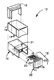
Fi_g. 1 is a ~~ersfective exploded assembly diagram of
a sirzgl_e-port mo~:~rlar connect or_ embodiment of the present
vr~,veit 1_or_ P
Fig. 2 is a side vi ew of_ t=he front and back: inser t
halves used in tuc rnoc:ul<tr connector of Fig. 1;
CA 02266995 1999-03-25
-6-
Fig. 3 is a side view of the front and back. insert
halves of Fig. 2 before being joined together to illustrate
which structures belong to each part;
Fig. 4 is a side view of the back insert halves of Figs.
1-3 and is intended to show that the wire connections rise
vertically within the plastic insert body and then turn
pezpendicular to run parallel with a motherboard the modular
connector may be mounted to. The left~ends of the conductors
in the diagram are curled back under to forma set of four
spring wire contacts to an RJ-45 jack;
Fig. 5 is a rear view of the back insert halves of Figs.
1-4 with the spring wire contact parts laid flat for the
diagram so that critical bends and kinks in the wire can be
better illustrated;
Fig. 6 is a side view of the front insert halves of
Figs. 1-3 and is intended to show that the wire connections
rise vertically within the plastic insert body and then turn
perpendicular to run parallel with a motherboard the modular
connector may be mounted to. The left ends of the conductors
in the diagram are curled back under to form another set of
spring wire contacts to an RJ-45 jack;
Fig. 7 is a rear view of the front insert halves of
Figs. 1-3 and 6 with the spring wire contact parts laid flat
for the diagram so that critical bends and kinks in the wire
can be better illustrated;
Fig. 8 is a schematic diagram of a DC blocking and
filter-capacitor circuit, as may be required in the coupling
of a PHY device to a cable medium in a 100BASE-T network
application, and that may be implemented within the
integrated signal conditioning part of any of the molded
inserts shown in Figs. 1-5;
Fig. 9 is a schematic diagram of a DC blocking and
series choke circuit, as may be required in the coupling of a
PHY device to a cable medium in a 100BASE-T nztwork
p > CA 02266995 2004-03-15
-?-
application, and that may be implemented within the
integrated signal conditioning part of any of the molded
inserts shown in Figs. I-5; and
Fig. 10 is a schematic diagram of a common mode choke
eizcuit, as may be required in the coupling of a PHY device
to a cable medium in a 100BASE-T network application, and
that may be implemented within the integrated signal
conditioning part o~ any of the molded inserts shown in Pigs.
1-5.
15 E ED
Fig. 1 illustrates a single-port printed-circuit-board
(PCB) mount modular connector embodiment of the present
invention, referred to herein by~the general reference
numeral 10. The modulaz connector 10 comprises a snap-in
insert assembly 12 that installs into a back end of a plastic
housing 14 and solders down to a PCB. A metal Faraday shield
16 covers the top, sides and back of the assembled insert 12
and housing 14 and grovides for electromagnetic-radiation
(EMR) protection. A tab 17 is intended to be soldered to a
groundplane of the PCB. A conductive flexible gasket 18 is
used to collar the front end of the assembled housing 14 and
shield I6 and provide R,T-45 jack grounding by bridging the
small distance to an installed jack. For further details of
this construction, see, United States Patent 5,64?.765.
issued July 15, 1997, to Haas, et al.
A group of spring connectors 20 passes through a hole 21
in a dividing wall within the housing 14 to ultimately
CA 02266995 1999-03-25
-s-
connect with any RJ-45 plugged in from the front. The RT-45
connection system is an industry standard and is ubiquitous
in the data network industry. The group of spring connectors
20 provides for eight industry defined circuit connections
that pass through a plastic insert body 22.
The typical RJ-45 connection to a data network is part
of the physical interface layer and requires a modest amount
of signal conditioning. It is critical to the present
invention that such signal conditioning be implemented
. entirely within the volume of the insert body 22, and
especially not off-connector on the PCB or in a "dog-house"
back extension. The pin-out, pin placements, and overall
form factor of the modular connector 10 are critical because
it must the be form, fit, and function equivalent to
preexisting PCB's that were designed for prior art modular
connectors. The point of mounting the signal conditioning
inside the insert body 22 is to save the PCB real estate that
would otherwise be needed or not available, and to gain the
F.t~t-related advantage of being inside the Faraday shield 16.
Fig. 2 shows that the insert body 22 actually comprises
a front insert half 24 and an back insert half 26, both of
which are made from a plastic with good dielectric
characteristics at near microwave frequencies.
Fig. 3 shows how the front insert half 24 and back
insert half 26 are joined together. The front insert half 29
supports spring connection jacks J1, J3, J5, and J7 at the
top, and PCB mounting pins P1, P3, P5, and P7 at the bottom.
Such PCB mounting pins are on 0.100 inch centers and phosphor
bronze 510 spring temper 0.014 inch material is used for all
of J1-P1 through J7-P7. The back insert half 26 supports
spring connection jacks J2, J4, J6, and J8 at its top, and
PCB mounting pins P2, P4, P6, and P8 at its bottom.
Such PCB mounting pins are also on 0.100 inch (2.54 mm) centers,
but staggered 0.050 inch (1.27 mm) relative to PCB mounting pins
P 1, P3, P5, and P7.
CA 02266995 2004-03-15
-9-
Phosphor bronze 510 spring temper 0.014 inch (0.36mm) wire material is used
for all of
J2-P2 through J8-P8.
Figs. 4-7 show details of how the wire material for J1-P1 through J8-P8 is
bent
and kinked in order to make the necessary connections and to inject controlled
inductances and capacitances respectively between J1-J8 and P1-P8. The
techniques
used here are borrowed from ultra high frequency (UHF) and microwave practice
where
sections of transmission lines are used to match impedances, build inductive
chokes,
and implement various kinds of low-pass, bandpass, and high pass filter
networks. Four
reactive components L1-L4 are identified which have critical run lengths that
are kinked
nearer to an adjacent conductor within front insert half 24 and back insert
half 26. The
separation distance, the run length, and the dielectric between are all
independent
variables that will affect the reactive impedances of L1-L4.
Referring now to Figs. 4 and 5, for an exemplary RJ-45 style modular
connector,
a dimension "dl" is about 0.450 inches (11.4 mm), "d2" is about 0.500 inches
(12.7
mm), "d3" is about 0.125 inches (3.175 mm), "d4" is about 0.625 inches (15.9
mm),
and "d5" about 0.625 inches (15.9 mm). A plastic keeper 27 prevents the spring
connectors from roaming too much while the assembly 12 is outside the housing
14.
Referring now to Figs. 6 and 7, for the same exemplary RJ-45 style modular
connector, a dimension "d6" is about 0.4375 inches (11.11 mm), "d7" is about
0.500
inches (12.7 mm), "d8" is about 0.500 inches (12.7 mm), and "d9" is about
0.625 inches
(15.9 mm).
Fig. 8 represents a DC blocking and filter-capacitor circuit 120 for coupling
a
PHY device through the PCB pins Pl-P6 to a cable medium in a 100BASE-T network
application through RJ-45 jack connections J1-J8. Such DC blocking and filter-
capacitor circuit 120 may be implemented within the integrated signal
conditioning part
of any of the molded inserts.
f
c L
CA 02266995 2004-03-15
-10-
Fig. 9 represents a DC blocking and series choke circuit
130 for coupling a PHY device through the PCB pins P1-P6 to a
cable medium in a 100BA5E-T network application through RJ-45
jack connections J1-J8. Such DC blocking and series choke
circuit 130 may be implemented within the integrated signal
conditioning part of any of the molded inserts.
Fig. 10 represents a common-mode choke circuit 140 for
coupling, e.g., a PHY device, through the PCB pins P1-P6 to a
cable medium in a 100BASE-T network application through RJ-45
jack connections J1-J8. Such common-mode choke circuit 140
may be implemented within the integrated signal conditioning
part of any of the molded inserts.
Fast Ethernet 100BASE-TX uses two pairs of category-5
balanced cable, or two pairs of 150 ohm shielded balanced
cable (as defined by ISO/IEC 11801). Fast Ethernet 1QOBASE-
FX uses two mufti-mode fibers as defined by ISO 9314. Fast
Ethernet 100BASE-T4 uses four pairs of category-3, -4 or -5
balanced cable (as defined by TSO/IEC 11801). In each case,
the length of a twisted-pair segment, from computer to wiring
closet, may be up to 100 meters (328 feet). This distance is
identical to that used by lOBASE-T links. Cable bundles such
as 25-pair cables cannot be used with 100BASE-T. There is no
provision for coaxial cable support or bus wiring methods. A
100BASE-TX system is similar to lOBASE-T in that one pair is
used to transmit while the other pair is used to detect a
data packet collision. This system defines a half-duplex
link. The physical properties of transmission are more
difficult to deal with at one hundred Mbps than at ten i4bps.
Therefore, better cable, connectors and jacks, and more
sophisticated transmission encoding must be used. Unshielded
cable must conform to rather rigorous category-5
specifications. The transmission scheme uses a block-code
known as "4B/SB,u creating a transmission frequency of one
CA 02266995 2004-03-15
-lI-
hundred twenty-five t~ia. The 100BASE-T4 'PHY' is designed to
work with category-3 cables tEthernet). Such cables usually
have poor noise responses above twenty-five l~iz and will not
meet FCC or European emission standards. Four pairs of
category-3 wire must be used to get satisfactory results,
e.g., the signal is split amongst the wire pairs and encoded
using a block code'known as '886T'. The resulting Iink can
be up to one hundred meters tthree hundred twenty-eight feet)
long, and 25-pair bundle cables cannot be used.
Although the present invention has been described in
terms of the presently preferred embodiments, it is'to be
understood that the disclosure is not to be izrterpreted as
limiting. Various alterations and modifications will no
doubt become apparent to those skilled in the art after
having read the above disclosure. Accordingly, it is
intended that the appended claims be interpreted as covering
all alterations and modifications as fall within the true
spirit and scope of the invention.