Note : Les descriptions sont présentées dans la langue officielle dans laquelle elles ont été soumises.
CA 02268576 1999-04-12
- 1 -
ELECTRONIC SWITCH RELAY
FIELD OF THE INVENTION
The present invention relates to switching
circuits, and more particuharly to a relay utilizing
electronic switching devices.
BACKGROUND OF THE INVENTION
The common assignee of the subject application is
an industry leader in the design and manufacture of
ultrasonic measurement devices. Such ultrasonic measurement
devices measure the distance between an object and a
transducer by sending a high frequency pulse to the object
and capturing echoes reflected by the object. By measuring
the delay between the transmission of the high frequency
pulse and the reception of the echo(s), the distance
between the object and the transducer is determined.
In many applications, the ultrasonic device will
include several transducers. Multiple ultrasonic
transducers allow multiple distances to be measured at the
same time. The transducers are coupled to a single
electronic control circuit through a series of relays. The
relays function as a multiplexer. A transducer is selected,
i.e. coupled to the electronic circuit, by activating the
associated relay, while the other relays serve to isolate
the unselected transducers, thereby preventing cross-talk
or interference between transducers. Conventional relays
are able to switch high currents and voltages as both
alternating current (AC) and direct current (DC).
CA 02268576 1999-04-12
- '2 -
Conventional electromechanical relays also feature a very
high galvanic isolation in the order of 1012 Ohms. The high
degree of isolation facilitates multiplexing multiple
transducers without giving rise to significant cross-talk
between transducers.
To improve the performance of the ultrasonic
measurement devices, a temperature sensing circuit 204 is
included. Temperature changes in air, gas, water, liquid;
etc. will affect the speed of the ultrasonic sound waves,
and the temperature sensing circuit allows the effects of
temperatures to be taken into account. The temperature
sensing circuit measures the temperature inside the
transducers, and generates a current proportional to the
absolute temperature (1 uA/°K). Because the output from the
sensing circuit comprises a current having a typical value
between 233uA for -40°C and 423uA for +150°C, it is critical
that leakage currents from the other transducers be
carefully controlled, otherwise the temperature readings
will be inaccurate. For many applications, the ultrasonic
measurement device will utilize 10 ultrasonic transducers.
Consequently, in order to accurately read a temperature
sensing circuit the leakage current contribution from all
the transducers must not exceed O.luA, otherwise, the
leakage currents may begin to affect the reading from the
temperature sensing circuit for the active transducer.
Conventional electromechanical relays utilize
mechanical contacts for switching and isolation. While
electromechanical relays are capable of providing the
required level of isolation between the transducers, the
operating life of the relay depends on the mechanical
contacts. Repetitive switching of an electromechanical
relay causes the contacts to wear. For certain applications
CA 02268576 1999-04-12
- 3 -
of the ultrasonic measurement device, such as grain level
monitoring in silos or liquid chemical measurement in a
tank, the contacts are more susceptible to degradation due
to airborne dust particulate or caustic chemical vapours.
In such industrial applications, the chemical vapours will
tend to oxidize or ionize the conductive coatings which are
applied to the surfaces of the contacts. As the integrity
of the contacts deteriorates the current is not able to
flow through the relay. As a result, echo and temperature
measurements cannot be read. It has been found-that in an
industrial application with the presence of ammonia vapour,
conventional electromechanical relays need to be replaced
as soon as 2 months for the ultrasonic measurement device
to function properly. Another drawback of electromechanical
relays is the switching noise which accompanies the
actuation of the contacts.
Accordingly, there remains a need for a suitable
replacement for conventional electromechanical relays which
provides the isolation characteristics of electromechanical
devices while at the same time is resistant to the effects
of harsh environments.
BRIEF SUMMARY OF THE INVENTION
The present invention provides an electronic
relay which utilizes semiconductor switching devices, such
as MOSFET's, thereby eliminating the need for mechanical
relay switches and includes an arrangement which minimizes
leakage currents in the switching devices thereby achieving
a high degree of isolation comparable to existing
electromechanical devices.
The present invention is particularly suited for
application in ultrasonic measurement devices designed and
CA 02268576 1999-04-12
- 4 -
manufactured by the common assignee of the present
application. Such ultrasonic measurement devices measure
the distance between an object and a transducer by sending
a high frequency pulse to the object and capturing echoes
reflected by the object. By measuring the delay between
the transmission of the high frequency pulse and the
reception of the echo(s), the distance between the object
and the transducer is determined. In many applications, the'
ultrasonic device will include several transducers
connected to a single electronic control circuit through a
series of relays. The relays function as a multiplexer and
a transducer is selected, i.e. coupled to the electronic
circuit, by activating the associated relay.
An object of the present invention is to provide
an electronic relay which can replace conventional
electromechanical relays and improve durability and
reliability. The electronic relay according to the present
invention exhibits the following features: the capability
to switch high and low voltage alternating current (AC),
and the capability to switch low voltage (negative) direct
current (DC). In the context of an ultrasonic measurement
device, the high AC voltage switching capability is needed
for the ultrasonic transmit functions. The low AC voltage
switching capability is needed for ultrasonic receive
functions and the negative DC switching capability is
needed for the temperature measurement function.
The electronic relay according to the invention
comprises semiconductor (i.e. solid state) switching
devices which eliminate the need for mechanical contacts as
in conventional electromechanical relays. Advantageously,
the elimination of mechanical contacts makes the electronic
relay less sensitive to the effects of harsh operating
CA 02268576 1999-04-12
- 5 -
environments, thereby improving the operating life of the
device. Another feature of the electronic relay is the
elimination of the switching noise from the operation of
the mechanical contacts. In addition, the electronic relay
according to the invention does not suffer from contact
bounce and as a result higher scanning speeds are possible.
In a first aspect, the present invention provides
an electronic relay for selectively coupling a transducer
to an electronic circuit, the transducer including an
input/output port for receiving excitation signals from the
electronic control circuit and transmitting echo signals to
the electronic control circuit, said electronic relay
comprising: (a) a solid state switch having a first port
connected to the input/output port of the transducer, a
second port coupled to the electronic control circuit, and
means for actuating said switch to electrically connect the
input/output port of the transducer to the electronic
control circuit in an on-state and isolate the input/output
port from the electronic control circuit in an off-state,
said means for actuating being responsive to a control
signal from the electronic control circuit; (b) leakage
current control means coupled to said solid state switch
for controlling leakage current when said solid state
switch is open so that the transducer is electrically
isolated from the electronic control circuit.
In another aspect, the present invention provides
an electronic relay for selectively coupling a transducer
to an electronic circuit, the transducer including an
input/output port for receiving excitation signals from the
electronic control circuit and transmitting echo signals to
the electronic control circuit, said electronic relay
comprising: (a) a solid state switch having a first port
~
CA 02268576 1999-04-12
- 6 -
connected to the input/output port of the transducer, a
second port coupled to the electronic control circuit, and
means for actuating said switch to electrically connect the
input/output port of the transducer to the electronic
control circuit in an on-state and isolate the input/output
port from the electronic control circuit in an off-state,
said means for actuating being responsive to a control
signal from the electronic control circuit; (b) said means
for actuation comprising a resistor and capacitor network
coupled to said switch and having an input port for
receiving said control signal.
BRIEF DESCRIPTION OF THE DRAfnTINGS
Reference will now be made to the accompanying
drawings which show, by way of example, preferred
embodiments of the present invention, and in which:
Fig. 1 is a schematic representation of an
ultrasonic measurement device with an electronic relay
according to the present invention;
Fig. 2 is a schematic representation of a
transducer for the ultrasonic measurement device of Fig: 1;
Fig. 3 is a schematic representation of an
implementation of the electronic relay of Fig. 1;
Fig. 4 is a schematic representation of another
implementation of the electronic relay of Fig. 1;
Fig. 5 is a schematic representation of another
implementation of the electronic relay of Fig. 1; and
CA 02268576 1999-04-12
Fig. 6 is a schematic representation of another
embodiment of the electronic relay of Fig. 1.
DETAILED DESCRIPTION OF THE PREFERRED EMBODIMENTS
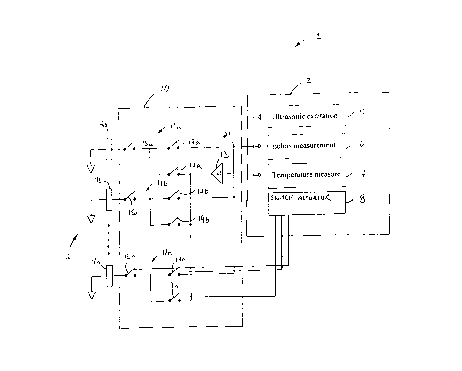
Reference is first made to Fig. 1 which shows an
ultrasonic measurement device 1 and an electronic relay
according to the invention. While the electronic relay
will be described in the context of the ultrasonic device
1, it is to be understood that the electronic relay
according to the present invention has wider applicability.
As shown in Fig. 1, the ultrasonic measurement
device 1 comprises a transducer module 2, a controller
module 3, and an electronic relay module 10 according to
the present invention. The ultrasonic measurement device 1
is subject of other patents and a brief overview is
provided as it pertains to the electronic relay 10, the
subject of the present invention. The ultrasonic
measurement device 1 provides a means for measuring the
distance between an object and the transducer module 2
(i.e. the device 1). Such a device has wide applicability
in applications as diverse as grain level measurement in a
silo to water level monitoring in flumes. The transducer
module 4 comprises a number of transducers 4, shown
individually as 4a, 4b .. 4n in Fig. l.,Each transducer 4
provides three functions as a transmitter for high
frequency pulses (i.e. pulses in the ultrasonic frequency
range), as a receiver for detecting echoes of the pulses
from the object and for temperature measurements. The
controller 3 includes an ultrasonic excitation module 5, an
echo measurement module 6, and a temperature measurement
module 7. The ultrasonic excitation module 5 provides the
excitation source for the transducers 4 to produce the high
frequency pulses. The high frequency pulses are directed
CA 02268576 1999-04-12
_ g _
towards the object and the reflections (i.e. echoes) from
the object are detected by the transducer module 2 and
converted into electrical signals which are processed by
the echos measurement module 6. in order to determine the
distance between the transducers 4 and the object.
The transducer 4 is shown in more detail in Fig.
2, and referring to Fig. 2, the transducer 4 comprises a
crystal 200 and an excitation coil 202. One side 202a of
the excitation coil is coupled to the crystal 2-00, and the
other side 202b of the coil 202 is coupled to the
excitation module 5 and the echo measurement module 6 in
the controller 3. Because the speed of sound is affected by
temperature changes, i.e. in air, gas, water, etc., each of
the transducers 4 preferably include a temperature sensor
circuit 204. The temperature sensor 204 generates an output
signal indicative of the temperature at the transducer 4.
The output signal is processed by the temperature
measurement module 7 for temperature compensation purposes.
The temperature sensor circuit 204 generates a current
proportional to the absolute temperature (1 uA/°K). Because
this current is typically very small, e.g. the current will
vary from 233uA for -40°C up to 423uA for +150°C, the
leakage currents through the switching elements in the
electronic relay need to be carefully controlled.
Furthermore, in many applications for the ultrasonic
measurement device 1 up to l0 ultrasonic sonic transducers
4 may be utilized. Consequently, when the temperature
sensor 204 in a transducer 4 is read, the leakage currents
associated with the switching devices for the other
transducers must not exceed O.luA, otherwise the reading
from the temperature sensor 204 may be affected. Therefore,
the leakage current from the switching devices for each
transducer 4 should not exceed 0.01uA for a device 1 with
CA 02268576 1999-04-12
_ g _
ten transducers 4. Based on a current polarization of 10
VDC for the temperature sensors 204, an isolation
resistance of 1G~ (i.e.~ lOV/O.OluA) is preferred. In
existing devices, electromechanical relay devices were used
to provide this degree of isolation. For further details of
the ultrasonic measurement device 1 reference should be
made to U.S. Patent Nos. 4,596;144 and 4,992,998 owned by
the common assignee of the subject application. In the
present invention, the electronic relay module 10 comprises
a solid state design. .
Referring back to Fig. 1, the electronic relay
module 10 comprises a switching module 11 for each of the
transducers 4 and a unity gain amplifier 13. In Fig. 1, the
switching modules 11 are shown individually as lla, llb,...
lln. Each.switching module 11 comprises a first switch 15,
a second switch 17 and a third switch 1-9. In Fig. 1, the
first, second and third switches are shown individually as
15a, 15b,... 15n, 17a, 17b,... 17n, and 19a, 19b,... 19n,
respectively. One terminal of each of the first switches 15
is coupled to the respective transducer 4. The other
terminal of the first switch 15 is coupled to a terminal of
the second switch 17 and a terminal of the third switch 19.
The input of the unity gain amplifier 13 is coupled to the
other terminal of each of the second switches 17. The input
of the amplifier 13 is also coupled to the output of the
excitation module 5, the input of the echo measurement
module 6 and the input of the temperature measurement
module 7. The output of the unity gain amplifier 13 is
connected the other terminal of each of the third switches
19. The actuation, i.e. opening and closing, of the
switches 15, 17, 19 is controlled by a switch actuator 8 in
a manner as will be described below.
CA 02268576 1999-04-12
- 10 -
It is a feature of the present invention that the
switching elements 15, 17, 19 are implemented using
semiconductor, i.e. solid state, devices. Semiconductor
switching devices have the advantage of eliminating the
mechanical contacts. However, semiconductor devices are
susceptible to leakage currents which can compromise the
isolation of the inactive transducers 4. For example, if
the switching elements 15, 17, 19 are implemented using
MOSFET (Metal Oxide Field Effect Transistors), there will
be a certain current leakage that is proportional to the
drain-source voltage when the transistor is in a non-
conductive state. An equivalent leakage resistor current
is given by the expression ,Vd$/Ileaxage ~ For a typical MOSFET
device, the leakage resistance is often in range 10 MS2 to.
40 MS2. Unfortunately, the leakage resistance tends to
decrease at high temperatures thereby causing an increase
in the leakage current and a decrease in the isolation
between the source and drain.
For an ultrasonic measurement device 1 having two
transducers 4, it has been found that while the leakage
currents from MOSFET switching devices result in some
compromises, performance is not adversely affected.
However, the benefits of the solid state switching devices
are diminished by the increases in the leakage currents as
the number of the transducers 4 is increased. Accordingly,
the electronic relay 10 according to the present invention
includes an arrangement for eliminating or at least
reducing leakage currents to negligible levels.
According to this aspect of the invention, the
third switches 19 and the unity gain amplifier 13 are
provided to minimize or eliminate the leakage currents
through the second switches 17 which is open to isolate the
CA 02268576 1999-04-12
- 11 -
currently inactive transducers 4. As will now be
described, the third switches 19 and amplifier 13 generate
a null voltage across the open switches 17 in order to
minimize the leakage currents. Referring to Fig. 1, if
transducer 4a is activated for excitation or echoes
measurement, then the first 15a and second 17a switches are
closed, while the first 15 and second 17 switches for the
remaining transducers 4b to 4n are open for isolation. To
eliminate the leakage currents through the open second 17a
to 17n switches, the respective third switches.l9b to 19n
are closed and the third switch 19a is open. The unity gain
amplifier 13 amplifies the current without modifying the
voltage. This arrangement of open and closed switches
causes the voltage at the input to the amplifier 13 and at
one terminal of each of the second switches 17b to 17n
(i.e. node 21) to be reproduced at the output of the
amplifier 13 and at the other terminal of each of each of
the second switches 17b to 17n through the respective
closed third switches 19b to 19n. The result is that a null
voltage is generated across the respective open switches
17b and 17n and the leakage current is zero. Similarly for
the active transducer 4a, a differential voltage of zero is
produced across the third switch 19a so that the leakage
current of the open switch 19a is also zero.
It will be appreciated that to obtain a perfectly
null voltage and leakage current the amplifier 13 would
theoretically need to have a perfect unitary gain with no
voltage offset. In a practical system, the unity gain
amplifier 13 will comprise an operational amplifier, i.e.
op-amp, having the highest impedance that is possible and
having a voltage offset as low as possible. Operational
amplifiers having a 100uV maximum offset or less are
readily available, for example, op-amp model LT1078
' CA 02268576 1999-04-12
- 12 -
manufactured by Linear Technology. Since the MOSFET
transistors will have at least lOMS2 minimum at the high
temperature, the resulting leakage current will be 10 pA
(i.e. 100 uV / 10 MS2) .
Better performance can be achieved by utilizing
a chopper stabilized op-amp. Chopper stabilized op-amps
typically have an offset voltage under luV. This would
result in a leakage current as low as O.lpA which is
comparable to electromechanical relays. In both cases,
i.e. 10 pA or 0.1 pA, the leakage current is small enough
that the reading of a transducer is not affected or the
error from a temperature sensor is not more than 0.1°C based
on a luA/°C or luA/°K output from the sensor 204.
In the case where the transducer 4 includes an
internal decoupling capacitor 206 (Fig. 2), the unity gain
amplifier 13 should still be able to force a null voltage
across the open switches if the series of first switches
15a to 15n were removed and replaced by short circuits, for
example, leaving second switches 17b to 17n and third
switch 19a described above. However, if the transducers 4
exhibit a primarily inductive characteristic, then the
amplifier 13 will not be able to force a DC voltage because
the inductors will act like a short circuit to ground.
Accordingly, the first switches 15 are provided to allow
amplifier 13 to force a null voltage across the second
switches 17. It will be understood that controlling the
leakage currents in the second switches 17 also has the
effect of blocking the leakage currents in the first
switches 15, and therefore it is not necessary to also
generate a null voltage across the first switches 15.
CA 02268576 1999-04-12
- 13 -
Having described the electronic relay 10, three
implementations of the electronic relay 10 will now be
described. In the following description, the
implementations of the electronic relay are provided for a
ultrasonic measurement device utilizing two transducers. It
will however be understood that the implementations are
suitable for N transducers.
Reference is made to Fig. 3, which shows a first
implementation of an electronic relay 100. Theelectronic
relay 100 comprises a unity gain amplifier stage 110 and
first 120 and second 130 switching elements for each of the
transducers 4. The first switching element 120 is used to
control the transducer 4, and the second switching element
130 is used to control the leakage currents in the
switching elements which are isolating one of the
transducers 4. In this implementation, the electronic relay
100 utilizes MOSFET transistors for the switching elements
120; 130. Since a MOSFET can only switch continuous
current, two transistors are utilized for each switching
element to order to handle alternating current.
The first switching element 120 comprises first
Q1 and second Q2 MOSFET (N-channel) transistors, and a
photo-voltaic coupler 121 or PVC coupler. The coupler 121
is used to generate an isolated voltage which is applied
across the source and gate terminals of the transistors Q1
and Q2, and provides the voltage to enable the gates of the
MOSFET transistors.
As shown in Fig. 3, the source terminals of the
transistors Q1 and Q2 are tied together, and the gate
terminals.are also tied together. The source terminals of
Q1 and Q2 are connected to the negative output terminal of
CA 02268576 1999-04-12
- 14 -
the coupler 12I and the gate terminals of Q1 and Q2 are
connected to the positive output terminal of the coupler
121. One of the control terminals of the coupler 121 is
connected to a switching contro_1 output 122 from the switch
actuator 8. The other control terminal of the coupler 121
is connected to signal ground through a resistor Rl. The
coupler 121 is used to generate a floating voltage high
enough to drive the gates and turn on the,transistors Q1
and Q2. The coupler 121 should be able to provide an output
current of approximately lOuA. Typical PVC type couplers
include a JFET (Junction Field Effect Transistor) on the
output which acts to short the gates of the transistors Ql
and Q2 when the coupler 121 is off.
The second switching element 130a comprises first
Q3 and second Q4 MOSFET (N-channel) transistors and another
PVC coupler 131. As shown in Fig. 3, the source terminals
of the transistors Q3 and Q4 are' tied together and
connected to the negative output terminal of the opto-
coupler 131. The gate terminals of transistors Q3 and Q4
are also tied together and connected to the positive output
terminal of the of the coupler 131. The control terminal of
the coupler 131 is connected to the~positive voltage rail
V~~ and the other control terminal is coupled to the
resistor R1 through a diode D1. With this arrangement, the
transistors Q3 and Q4 are turned on, i.e. switch 130a is
closed, when a signal to turn OFF, i.e. open the switch
120a, is received from the control input 122. Conversely,
the transistors Q3 and Q4 are turned OFF when a signal to
turn ON the switch 120a is issued on the control input 122.
The first switching element 120b for the second
transducer 4b is arranged in a similar fashion to the first
switching element 120a. The switching element 120b
CA 02268576 1999-04-12
- 15 -
comprises first Q5 and second Q6 MOSFET transistors and an
opto-coupler 123. The source terminals of the transistors
Q5 and Q6 are tied together and connected to the negative
output terminal of the coupler 123. The gate terminals of
transistors Q5 and Q6 are tied together and connected to
the positive output terminal of the coupler 123. One
control terminal of the coupler 123 is connected to a
control output 124 from the switch actuator 8. The other
control terminal of the coupler 123 is connected to signal
ground through a resistor R2.
The second switching element 130b for the second
transducer 4b is arranged in a similar fashion to the
switching element 130a and comprises first Q7 and second
Q8 MOSFET transistors and an opto-coupler 132. The source
terminals of the transistors Q7 and Q8 are tied together
and connected to the negative output terminal of the opto-
coupler 132. The gate terminals of transistors Q7 and Q8
are also tied together and connected to the positive output
terminal of the coupler 132. The control terminal of the
opto-coupler 132 is connected to the positive voltage rail
V~~ and the other control terminal is coupled to the
resistor R2 through a diode D2. With this arrangement, the
transistors Q7 and Q8 are turned on, i.e. switch 130b is
closed, when a signal to turn off, i.e. open the switch
120b, is received from the control input.124.
In this embodiment, the first switching elements
120 are used to enable the respective transducer 4 for
excitation and echo measurement. The second switching
elements 130, on the other hand, operate together with
unity gain amplifier stage 110 to control the leakage
currents through the transistors in the switching elements.
CA 02268576 1999-04-12
- 16 -
As shown in Fig. 3, the amplifier stage 110
comprises a first op-amp 111 and a second op-amp 112. The
first op-amp 111 is configured as a unity gain amplifier.
The positive and negative inputs of the op-amp 111 are
coupled through a resistor R6 to the node formed by the
connection of the outputs of the first and second switching
elements 120a and 120b. The second op-amp 112 is configured
as a voltage follower to supply a low impedance output to
'the switching elements 130a and 130b. The positive terminal
of the op-amp 112 is tied to the output of the first op-amp
111. The negative terminal is coupled to a leakage control
node 113 through a feedback resistor R3. The leakage
control node 113 is formed from the connection between the
drain terminals of transistors Q4 and Q8 in the respective
switching elements 130. As shown in Fig. 3, the negative
and positive input terminals of the op-amp 112 are coupled
through diodes D3 and D4. The output of the op-amp 112 is
coupled to the leakage current control node 113 through a
resistor R4. The resistor R4 functions as protection device
to limit current.
In operation, when transistors Q1 and Q2 are
turned OFF, i.e. opened, transistors Q3 and Q4 are turned
ON and a voltage is forced on the source of transistor Q2.
Because the source of transistor Q1 is at a lower potential
then the drain of transistor Q1, the protection diode in
transistor Q1 will block the current from ground through
the first transducer 4a. Therefore, even if the transducer
4 represents a short circuit to DC (i.e. the transducer 4
does not include a decoupling capacitor), the leakage
current through transistor Q1 is controlled. The protection
diode in the transistor Q1 effectively replaces the first
switch 15 in the arrangement shown in Fig. 1. Since
transistor Q1 becomes a high impedance, a voltage can be
' CA 02268576 1999-04-12
- 17 -
forced on the source of transistor Q2 to control its
leakage current. Through the operation of the unity gain
amplifier stage 110 the potential difference between the
source and the drain of transistor Q2 becomes zero.
Consequently, the leakage current in transistor Q2 will be
null.
It will be understood that the offset voltage of
the op-amp 111 will affect the precision of the "zero volt"
potential between the source and the drain of_transistor
Q2, which in turn may lead to some leakage current from
transistor Q2. Since the leakage current is DC, the leakage
current will not affect operation of the transducer 4 and
the echos measurement module 6, which operate using AC
signals. However, if the resulting leakage current is too
high, the operation of the temperature measurement module
7 could be affected since the temperature module 7 responds
to DC signals from the sensor 204 (Fig. 1).
Conversely, when transistors Q1 and Q2 are
closed, i.e. turned ON to communicate with the associated
transducer 4, the transistors Q3 and Q4 are opened or
turned OFF. The first op-amp 111 again inputs the voltage
signal from the transducer signal node 109 and the signal
is reproduced by the second op-amp 112 at the leakage
current control node 113. As described above, the output of
the second op-amp 112 is a low impedance output. With
transistor Q2 turned ON, the resulting potential difference
across the turned OFF transistors Q3 and Q4 is zero, i.e.
the leakage control node 113 is at the same voltage level
as the transducer signal node 109. As a result, the leakage
current in the transistors Q3 and Q4 will be zero.
' CA 02268576 1999-04-12
- 18 -
Referring to Fig. 3, diodes D5 and D6 are
provided to protect the inputs the first op-amp 111 and the
positive input of the second op-amp 112. During the
excitation, there is a 400 VAC (peak-to-peak) present at
node 109, but this AC voltage is only used to excite the
transducer. During the taking of a reading, a low level AC
voltage is present at the node 109. The unity gain
amplifier 111 follows the voltage at node 109, but the
ability of the amplifier 111 to null the voltage for all
positive and negative excursions will depend on the
characteristics of the transducer (i.e. if the transducer
includes a decoupling capacitor). During the temperature
reading stage, a negative DC voltage is present at the node
109 and the leakage currents in the MOSFETs are effectively
controlled.
The negative input of the second op-amp 112 is
protected by the resistor R3 and diodes D3 and D4. The
diodes D3 and D4 are coupled to the low impedance output of
the first op-amp 111. As a result stray capacitance at the
inputs of the op-amp 112, the feedback through resistor R3
will be delayed. Typically, a capacitor would be added in
parallel to resistor R3 for compensation. It is however
preferable to not include such a capacitor since resistor
R3 is provided for protection and a capacitor in parallel
would act as a short circuit for high frequency AC signals.
(High frequency AC signals are used for the transducers 4.)
Instead for compensation, the op-amp 112 includes a snubber
circuit comprising a capacitor C1 and resistor R5. As shown
in Fig. 3, the snubber circuit is coupled to between the
positive and negative inputs of the op-amp 112. The snubber
circuit's function is to damp any oscillation between the
inputs of the op-amp 112. The capacitor C1 is selected so
CA 02268576 1999-04-12
- 19 -
that it appears as a short circuit at the oscillation
frequency.
As also shown in Fig. 3, a capacitor CS is
provided at the output of each transducer 4a, 4b. The
function of the capacitors C9 is filter any noise which
emanates from a transducer 4 which is not currently
selected, i.e. isolated by the associated switching element
120. The stray capacitance between the source and drain of
each MOSFET Q1, Q2 (or Q3 and Q4) in the -turned-off
switching element 120 can transmit noise from the
unselected transducer 4 which in turn could corrupt the
output being read from the currently selected transducer 4.
The capacitor Cs preferably comprises a ceramic type
capacitor.
Typical component values for the electronic relay
100 of Fig. 3 are as follows:
D1 to D6 1N4148
Q1 to Q8 MTP3N50E
R1, R2 392 Ohms
R3, R6 300 KOhms
R5 4.02 KOhms
R4 1.88 KOhms
C1 1 uF
PVC's PVI1050
Op-amp LT1078
Cs 220 pF, 500 Volt
Reference is next made to Fig. 4, which shows in
schematic form a second embodiment of an electronic relay
200 according to the invention. The electronic relay 200 is
very similar to the relay 100 described in Fig. 3, 'except
CA 02268576 1999-04-12
- 20 -
that the number of PVC couplers has been reduced by two. It
will be appreciated that eliminating the number of PVC
couplers can result in significant cost savings since the
PVC coupler represents the most expensive component in the
electronic relay. As will be described, the electronic
relay 200 utilizes more cost effective opto-couplers.
In Fig. 4, like reference numerals are used to
indicate like elements in the Fig'. 3.
Referring to Fig. 4, the electronic relay 200
comprises a unity gain amplifier stage 210, and first 220
and second 230 switching elements for each of the
transducers 4. The electronic relay 200 shown in Fig. 4 is
configured for two transducers 4a and 4b and the
corresponding first switching elements and second switching
elements are indicated individually as 220a; 220b and 230a,
230b, respectively. The first switching element 220 is used
to control the transducer 4; and the second switching
element 230 is used to control the leakage currents in the
switching element which is isolating one of the transducers
4. The electronic relay 200 also utilizes MOSFET
transistors for the switching elements 220, 230. Since a
MOSFET can only switch continuous current, two transistors
are utilized for each switching element in order to handle
alternating current.
The first switching element 220 comprises first
Q1 and second Q2 MOSFET transistors, and an opto-coupler
221. A PVC coupler 222 is shared between the pair of
switching elements 220a and 230a. The PVC coupler 222
comprises a known device, such as the PV11050 manufactured
by International Rectifier. The PV11050 features dual
photo-sensitive output ports (indicated by references 223
CA 02268576 1999-04-12
- 21 -
and 224 in Fig. 4) which are activated by a single LED
source. To turn ON the MOSFET transistors, the PVC coupler
222 needs to provide at least a 10 uA output, which is
within the specification of the PV11050 device. The opto-
coupler 221 comprises a integrated device such as the H11A1
which is available from a number of manufacturers. The PVC
coupler 222 and the opto-coupler 221 are used to generate
an isolated voltage which is applied across the source and
gate terminals of the transistors Ql and Q2.
As shown in Fig. 4, the source terminals of the
transistors Q1 and Q2 are tied together, and the gate
terminals of Q1 and Q2 are also tied together. The source
terminals of Q1 and Q2 are connected to the negative output
terminal of the first port 223 on the coupler 222 and the
gate terminals of Ql and Q2 are connected to the positive
output terminal of the same port 223. The control terminal
of the PVC coupler 222 is coupled through a resistor Rl3 to
the control output of an opto-coupler 231 which is
connected to the switching control output 122 from the
switch actuator 8. One input of the opto-coupler 221 is
coupled to the resistor R13 through a protection diode D7
and the other input is tied to the positive supply rail Vac.
The output port of the opto-coupler 221 is coupled to the
tied-together gates and sources of the transistors Q1 and
Q2 as shown. The tied-together sources of transistors Q1
and Q2 are also connected to another terminal on the opto-
coupler 221 through a resistor R11.
Similarly, the second switching element 230a
comprises first Q3 and second Q4 MOSFET transistors and the
opto-coupler 231. The source terminals of the transistors
Q3 and Q4 are tied together and connected to the negative
output terminal of the second port 224 on the PVC coupler
' CA 02268576 1999-04-12
- 22 -
222. The gate terminals of transistors Q3 and Q4 are also
tied together and connected to the positive output terminal
of the second port 224. As shown in Fig. 4, the gates and
sources of the transistors Q3 and Q4 are also coupled to
the output port of the opto-coupler 231. The tied-together
sources of transistors O3 and 04 are also coupled to
another terminal of the opto-coupler 231 through a resistor
R12.
The arrangement of the PVC coupler 222 and the
two opto-couplers 221 and 231 toggles the first 220a and
second 230a switching elements ON and OFF in response to
the control signal from the switching control output 122 in
the switch actuator 8.
The first switching element 220b for the second
transducer 4b is arranged in a similar fashion to the first
switching element 220a. The switching element 220b
comprises first Q5 and second Q6 transistors, and an opto-
coupler 225. A PVC coupler 226 is shared between the pair
of switching elements 220b and 230b. The transistors Q5 and
Q6 are coupled to the opto-coupler 225 and the PVC coupler
226 with resistors R14 and R16 and diode D8 as described
above for the first switching element 220a.
The second switching element 230b for the second
transducer 4b is also arranged in a similar fashion to the
switching element 230a for the first transducer 4a. The
switching element 230b comprises first Q7 and second Q8
transistors, and an opto-coupler 232. The transistors Q7
and Q8 are coupled to the opto-coupler 232 and the PVC
coupler 226 with resistors R15 and R16 as described above
for the switching element 230a.
CA 02268576 1999-04-12
- 23 -
As shown in Fig. 4, the input control terminal of
the opto-coupler 232 is connected to the control output 124
from the switch actuator 8. When the second transducer 4b
is selected, the switch elements 220b and 230b are toggled
ON and OFF in response to the control signal on the switch
control line 124.
The first switching elements 220a, 220b are used
to enable the respective transducer 4 for excitation and
echo measurement. The second switching elements-230a, 230b,
on the other hand, operate together with the unity gain
amplifier stage 210 to control the leakage currents through
the transistors in the switching elements.
As shown in Fig. 4, the amplifier stage 210
comprises a first op-amp 211 and a second op-amp 212. The
first op-amp 211 is configured as a unity gain amplifier.
The positive and negative inputs of the op-amp 211 are
coupled through a resistor R10 to a node 109 formed by the
connection of the outputs of the first and second switching
elements 220a and 220b. The second op-amp 212 is configured
as a buffer which supplies a low impedance output to the
switching elements 230a and 230b. The positive terminal of
the op-amp 212 is tied to the output of the first op-amp
211. The negative terminal is coupled to a leakage control
node 113 through a feedback resistor R7. The leakage
control node 113 is formed from the connection between the
drain terminals of transistors Q4 and Q8 in the respective
switching elements 230. As shown in Fig. .4, the negative
and positive input terminals of the op-amp 212 are coupled
through diodes D3 and D4. The output of the op-amp 212 is
coupled to the leakage current control node 113 through a
resistor R8. The resistor R8 functions as a protection
device to limit current.
CA 02268576 1999-04-12
- 24 -
The electronic relay 200 shown in Fig. 4 operates
in the same fashion as the electronic relay 100 described
above with reference to Fig. 3. The electronic relay 200 is
suitable for the following application range: AC voltages
and negative DC voltage levels less than ~-15 VDC~.
As shown in Fig. 4, the electronic relay 200
includes capacitors Ce for filtering noise from the
respective transducers 4 which could be coupled to the
controller 3 through the stray capacitance between the
source and drain of the MOSFETs Q1, Q2 or Q5, Q6 as
described above for Fig. 3.
Typical component values for the electronic relay
200 of Fig. 4 are as follows:
D3 to D8 1N4148
Q1 to Q8 MTP3N50E
R11, R12, R14, R15 100 KOhms
R13, R16 392 Ohms
R7, R10 300 KOhms
R9 4.02 KOhms
C1 1 uF .
C8 220 pF, 500 Volt
PVC PVI1050
Opto-couplers H11A1
Op-amps LT1078
For the embodiments of the electronic relay 100
and 200 described above, the PVC couplers were utilized to
supply an isolated voltage to enable the gates of the
MOSFET transistors. This arrangement enables the MOSFET's
to switch ~DC and AC signals. However for the ultrasonic
transducers 4 used in the ultrasonic measurement device,
' CA 02268576 1999-04-12
- 25 -
the signals encountered for typical operation comprise AC
signals at a frequency greater than 1 kHertz and DC signals
less than 15 Volts and negative. Another embodiment of an
electronic relay 300 which is tailored for this operating
range is shown in Fig.~S. In the implementation for the
electronic relay 300 of Fig. 5, the opto-coupler devices
(e.g. 121, 131 in Fig. 3 and 221, 222 and 231 in Fig. 4)
and the MOSFET's in the second switching elements (i.e. 130
in Fig 3 and 230 in Fig. 4) have been replaced by a circuit
arrangement which utilizes bi-polar transistors and
operational amplifiers. This leads to significant cost
savings since the opto-coupler devices and to a lesser
extent the MOSFET transistors represent a significant
component costs in the electronic relay.
The electronic relay 300 in Fig. 5 is shown for
two transducers 4a and 4b, however, it will be understood
that circuit may be extended to N ultrasonic transducers.
Referring to Fig. 5, the electronic relay 300 comprises a
unity gain amplifier stage 310, a switching element 320, a
leakage control circuit 330, and a switching drive circuit
340 for each of the transducers 4. The switching element
320 is used to control the transducer 4 and the leakage
control circuit 330 is used to control the leakage currents
in the switching elements which are isolating a transducer
4 which is not active. The switching drive circuit 340a as
will be described below works together with the control
circuit 330 to eliminate the need for the PVC couplers by
providing an isolated voltage for switching the MOSFET
transistors in the switching elements 320.
The switching element 320a for the first
transducer 4a comprises first Q1 and second Q2 MOSFET (N-
channel) transistors. The drain of the first MOSFET Q1 is
' CA 02268576 1999-04-12
- 26 -
coupled to the transducer 4a and the drain of the second
MOSFET Q2 is coupled to the node 109. The sources of the
transistors Q1 and Q2 are tied together and connected to a
terminal of a capacitor C3 in the switching drive circuit
340a. The other terminal of the capacitor C3 is connected
a resistor R16 in the switching drive circuit 340a. This
terminal of the resistor R16 is also connected to the gates
of the transistors Q1 and Q2 which are tied together. The
other terminal of the resistor R16 is coupled to the
control output l22 of the switch actuator 8 and also to the
leakage control circuit 330a.
As shown in Fig. 5, the leakage control circuit
330 comprises an op-amp 332 and first Q9 and second Q10 bi-
polar transistors. The negative input of the op-amp 332 is
connected to the output. of the unity gain amplifier stage
310 at node 309. As shown in Fig. 5, the negative and
positive inputs of the op-amp 332 are connected to a pair
diodes D9 and D10. The diodes D9 and D10 are provided to
protect the inputs of the op-amp 332. The output of the op-
amp 332 is coupled to the base of the transistor Q9 through
a resistor R17. The emitter of the transistor Q9 is
connected to the lower voltage rail Vdd, and the collector
of Q9 is coupled to the positive input of the op-amp 332
through resistors R18 and R19 and a diode D11. The anode of
the diode D11 is also connected to the tied together
sources of the MOSFET transistors Q1 and Q2.
As shown in Fig. 5, the op-amp 332 also includes
a snubber circuit comprising a capacitor C5 and a resistor
R20 for compensation. The snubber circuit is coupled
between the positive and negative inputs of the op-amp 332,
and functions to damp any oscillation between the inputs of
' CA 02268576 1999-04-12
- 27 -
the op-amp 332. The capacitor C5 is selected so that it
appears as a short circuit at the oscillation frequency.
The collector of the second transistor Q10 is
connected to the base of the first transistor Q9, and the
emitter of Q10 is connected to the low voltage rail Vdd. The
base of the transistor Q10 is coupled through a resistor
R21 to the control output 122. The base of Q10 is also
coupled to the lower voltage rail Vdd through a resistor
R22. The primary function of the transistor-Q10 is to
enable/disable transistor Q9.
For the second transducer 4b, the second
switching element 320b, the leakage current control
circuit, and the switching drive circuit 340b are arranged
in a similar fashion. The switching element 320b comprises
first Q5 and second Q6 MOSFET transistors. The drain of the
first MOSFET Q5 is coupled to the transducer 4b and the
drain of the second MOSFET Q6 is coupled to the node 109.
The sources of the transistors Q5 and Q6 are tied together
and connected to a terminal of a capacitor C4 in the
switching drive circuit 340b. The other terminal of the
capacitor C4 is connected a resistor R23 in the switching
drive circuit 340b. This terminal of the resistor R23 is
also connected to the gates of the transistors Q5 and Q6
which are tied together. The other terminal of the resistor
R23 is coupled to the control output 124 of the switch
actuator 8 and also to the leakage control circuit 330b.
As shown in Fig. 5, the leakage control circuit
330b comprises an op-amp 333 and first Q11 and second Q12
bi-polar transistors. The negative~input of the op-amp 333
is also connected to the output of the unity gain amplifier
stage 310 at node 309. For protection, a pair of diodes D12
CA 02268576 1999-04-12
- 28 -
and D13 are provided across the negative and positive
inputs of the op-amp 333 as shown in Fig. 5. The output of
the op-amp 333 is coupled to the base of the transistor Q11
through a resistor R24. The emitter of the transistor Q11
is connected to the lower voltage rail Vdd, and the
collector of Q11 is coupled to the positive input of the
op-amp 333 through resistors R25 and R26 and a diode D14.
The anode of the diode D14 is also connected to the tied
together sources of the MOSFET transistors Q5 and Q6.
The op-amp 333 also includes a snubber circuit
for compensation comprising a capacitor C6 and a resistor
R27 as shown in Fig. 5. The capacitor C6 is selected so
that it appears as a short circuit at the oscillation
frequency.
The collector of the second transistor Q12 is
connected to the base of the first transistor Q11, and the
emitter of Q12 is connected to the low voltage rail Vdd. The
base of the transistor Q12 is coupled through a resistor
R29 to the control output 124. The base of Q12 is also
coupled to the lower voltage rail Vdd through a resistor
R29.
For the operation of the electronic relay 300, a
command signal of -12 Volts is outputted by the switch
actuator 8 on the control lines 122, 124 to turn OFF a
switch element 320 (i.e. isolate a transducer 4) and a
command signal of +12 Volts is outputted to turn ON a
switch element 320 (i.e. select a transducer 4 for
excitation and reading, or to input the temperature
compensation signal).
' CA 02268576 1999-04-12
- 29 -
Referring to Fig 5 and, in particular, to the
first switching element 320a and the switching drive
circuit 340a, when the command signal on the control output
122 is negative, i . a . -12 Volts, the capacitor C3 in the
switching control circuit 340a is charged at a negative
voltage relative to the sources of the MOSFET transistors
Q1, Q2. Even if a high voltage signal is applied by the
ultrasonic excitation module 5, the MOSFET transistors Q1
and Q2 will stay off because the capacitor C3 will maintain
a more negative voltage on the gates than on the sources of
the MOSFET's. Similarly, the MOSFET's Ql and Q2 in this OFF
state will block an AC output signal from the transducer
4a. If the temperature compensation module 8 attempts to
read the output signal from the temperature circuit 204
(Fig. 2), then the sources of the MOSFET's Q1 and Q2 are
pulled down to -11.4 Volts (i.e. -12 Volts plus the drop
across the protection diode for Q2). Consequently, the
transistor Q1 does not conduct if a negative continuous
voltage is applied on the drain with respect to the source
of the transistor Ql.
When a +12 Volt command signal is applied from
the control output 122 the protective diode for transistor
Q1 forces the voltage at the sources of transistors Ql and
Q2 to approximately 0.6 Volts (i.e. before transistor Q1
conducts). This in turn causes the transistors Q1 and Q2 to
conduct. In the conduction state, the voltage drop across
transistors Q1 and Q2 is virtually zero and the "On-state
impedance" for the switching element 320a will be two times
the resistance Ron for the transistor Q1 or Q2 (where
transistors Q1 and Q2 are matched) . For the transistor type
utilized for Q1 and Q2 in the switching element 320a, the
on-state impedance is less than six Ohms. This low
impedance is maintained as long as the sources of the
CA 02268576 1999-04-12
- 30 -
MOSFET transistors Q1, Q2 have a voltage which is less than
0 Volts DC. When the voltage level for a DC signal rises
above 8 Volts, the MOSFET's Q1, and Q2 will not conduct.
However, this does not present a significant problem
because the DC signal of interest for the ultrasonic
measurement device is the output signal from the
temperature sensor 204 (Fig. 2) and this signal is
typically -12V to OV. The differential voltage between the
gates and sources of MOSFETs Q1 and Q2 will be between 5 to
17 Volts. For the AC signals outputted to and inputted
from the transducer 4a, the capacitor C3 is continuously
charged and keeps the transistors Q1 and Q2 ON or in
conduction.
Because the temperature reading' from the
temperature sensor 204 (Fig. 2) is critical to the
operation of the ultrasonic measurement device 1, the
leakage currents from the transducers 4 which are not
selected must be minimized or eliminated. For the
electronic relay 300 of Fig. 5, the function of the bi-
polar transistor Q9 is to maintain a null potential
difference between the source and'the drain of the MOSFET
Q2 when transistor Q2 is in a non-conduction state. A~null
voltage across the non-conductive MOSFET Q2 or Q6 means
that the leakage current is also null. Accordingly, a
transducer 4 which is not selected will not introduce an
error in the temperature reading because of leakage current
from the MOSFET transistor Q2 or Q6.
In operation, a -12 Volt command signal is
applied on the control outputs 122, 124 to disable a
transducer 4 and a +12 Volt command signal is applied to
enable a transducer 4, i.e. the MOSFET's Ql and Q2 in the
switching element 320 are turned ON. Therefore, to disable
CA 02268576 1999-04-12
- 31 -
the first transducer 4a and select the second transducer
4b, a -12 Volt command signal is applied to the switching
drive circuit 340a for the first switching element 320a and
a +12 Volt command signal is applied to the switching drive
circuit 340b for the second switching element 320b. When
the -12 Volt command signal is applied, the transistor QlO
is turned OFF, and the voltage at node 109 is applied to
the anode of diode D11 via the unity gain amplifier 310,
the amplifier 332 and the transistor Q9. The output from
the op-amp 332 controls the transistor Q9 to produce a
voltage at the anode of diode D11 equal to the output of
the unity gain amplifier 310. The resistor R19 provides
feedback of the voltage at the anode of diode D11. When
the anode voltage of diode D11 equals the voltage at node
109, the leakage for the MOSFET Q2 will be null. This
results in a null leakage current flowing from the MOSFET
Q2. Since transistor Q9 is a bipolar transistor it cannot
handle AC voltages. It will however be understood that the
leakage needs to be controlled the temperature readings are
being taken, i.e. a low negative DC voltage level between
0 to -12V. The diode D11 is provided to disable the
transistor Q9 when the voltage level falls below -12V. The
leakage control circuit 330b for the second switching
element operates in a similar fashion when the second
transducer 4b is disabled.
As shown in Fig. 5, the electronic relay 300
includes capacitors Cs for filtering noise from the
respective transducers 4 which could be coupled to the
controller 3 through the stray capacitance between the
source and drain of the MOSFETs Q1, Q2 or Q5, Q6 as
described above for Fig. 3.
CA 02268576 1999-04-12
- 32 -
Typical component values for the electronic relay
300 of Fig. 5 are as follows:
D11, D14 BYD77G
D9, D10, D12, D13 1N4148
Ql, Q2, Q5, Q6 MTP3N50E
Q9, Q11 MPSA42
Q10, Q12 2N4401
R8 1.88 KOhms
R16, R23 . 10 MOhms
R19, R26, R30 300 KOhms
R18, R25 1.88 KOhms
R21, R22, R28, R29 200 KOhms
R 17 , R2 4 10 KOhms
R20, R27 4.02 KOhms
C5, C6 1 uF
C3 , C4 1 nF
CS 220 pF, 500 Volt
Op-amps LT1078
Reference is next made to Fig. 6 which shows
another embodiment of an electronic relay 400 according to
the invention. The electronic relay 400 is particularly
suited for an application comprising two transducers 4a and
4b. For such an arrangement, one of the transducers 4 will
be active, and therefore, it is necessary to only eliminate
the effect of the other switch in order to input a clean
reading from the associated transducer.
Referring to Fig. 6, the electronic relay 400
comprises first 420a and second 420b switching elements.
Each of the switching elements 420 includes a respective
isolation circuit 430a and 430b. The first switching
CA 02268576 1999-04-12
- 33 -
element 420a comprises first Qla and second Q2a (N-channel)
MOSFET transistors. As shown in Fig. 6, the source
terminals of transistors Qla and Q2a are tied together, and
the gate terminals of transistors Qla and Q2a are also tied
together. The drain terminal of transistor Q1a is coupled
to the transducer 4a, while the drain terminal of
transistor Q2a is coupled to the input/output line of the
controller 3. Similarly, the second switching element 420b
comprises first Qlb and second Q2b MOSFET transistors. The
source terminals of transistors Qlb and Q2b are tied
together, and the gate terminals of transistors Qlb and Q2b
are also tied together. The drain terminal of transistor
Qlb is coupled to the transducer 4b, while the drain
terminal of transistor Q2b is coupled to the input/output
line of the controller 3.
As shown in Fig. 6, the isolation circuit 430a
for the first switching element 420a comprises a capacitor
C7 and a resistor R31. The capacitor C7 is coupled across
the tied-together source and tied-together gate terminals
for the transistors Qla and Q2a. One terminal of the
resistor R31 is connected to the tied-together gate
terminals of transistors Qla and Q2a, and the other
terminal of the resistor R31 is connected to the control
output 122 from the switch actuator 8. Similarly, the
isolation circuit 430b for the second switching element
420b comprises a capacitor C8 and a resistor R32. The
capacitor C8 is coupled across the tied-together source and
tied-together gate terminals for the transistors Qlb and
Q2b. One terminal of the resistor R32 is connected to the
tied-together gate terminals of transistors Qlb and Q2b,
and the other terminal of the resistor R32 is connected to
the control output 124 from the switch actuator 8.
CA 02268576 1999-04-12
- 34 -
The electronic relay 400 shown in Fig. 6 allows
an AC voltage or a low negative voltage (i.e. in the range
0 to -15VDC) to be switched from the transducer 4. To
provide the ability to switch an AC voltage, the drive or
control voltage for the MOSFET's Q1 and Q2 needs to be
isolated. For the embodiments described above, isolation
was provided through the use of opto-couplers and the like.
For the electronic relay 400 shown in Fig. 6, isolation is
provided by the resistors R31 and R32 in the respective
isolation circuits 430a and 430b. The value for the
resistors R31 and R32 is high, typically 10 MOhms. While
the resistors R31 and R32 do not provide perfect galvanic
isolation, i.e. there will be some AC leakage, leakage
during the reading of the DC temperature signal is the most
critical. During the reading of the DC temperature signal,
the capacitors C7, C8 and the gates of the MOSFET's Ql, Q2
prevent leakage currents and possible corruption of the DC
signal level being inputted from the selected transducer 4.
During AC operation, i.e. for ultrasonic
excitation and echo measurement of a transducer 4, the
average voltage across the MOSFET's Q1, Q2 will be zero.
To excite and read the first transducer 4a, the switch
actuator 8 generates a +SVDC signal on control output 122
and a -12VDC signal on control output 124. The +5VDC on
control output 122 turns on the MOSFET's Qla and Q2a, and
the -12VDC on control output 124 turns off the MOSFET's Qlb
and Q2b in the second switching element 420b. If an AC
voltage appears at the drain of either MOSFET Qla or Q2a,
the MOSFET Qla or Q2a will stay on because the capacitor C7
maintains a +5VDC voltage across the gate and source
terminals of the MOSFET's Qla and Q2a.
CA 02268576 1999-04-12
- 35 -
To keep the MOSFET's Q1 and Q2 turned ON for the
transmission of any AC signal (i.e. excitation signal to
transducer 4 or echo measurement signal from the transducer
4), the RC constant for resistor R31 and capacitor C7 (and
resistor R32 and capacitor~C8) should be at least 10 times
greater than the period of the lowest frequency AC signal
applied to the transducer 4. To provide an additional
measure of protection, the values for the resistors R31,
R32 and capacitors C7, C8 are selected to give a RC
constant of at least 100 to 1000 times the period of the
lowest frequency AC signal. It will be understood that a
small RC constant will allow the capacitor C7 or C8 to
rapidly overcharge and lead to high voltage being applied
to the gates of the MOSFET's Q1, Q2 which could damage the
MOSFET's.
During DC operation, i.e. for reading the DC
temperature signal from the transducer 4, the maximum DC
voltage applied to the gate terminals of the MOSFET's Q1
and Q2 needs to be carefully controlled. For the selected
MOSFET devices, the voltage between the gate and source
terminals should.not exceed ~ 20VDC. For example, if a
+SVDC voltage is applied on control line 122 or 124 to turn
on the respective MOSFET pair Qla and Q2a or Qlb and Q2b,
then the voltage across the source and drain terminals
cannot be brought lower than -15VDC, otherwise the gate
could be damaged. If a voltage greater than +1 VDC (i.e.
+5 VDC minus the threshold gate voltage for the MOSFET,
typically 4 VDC), then both MOSFET transistors Q1 and Q2
would turn off and the switching element 420 would be
inoperable. Accordingly for DC operation, the control
voltage for activating the MOSFET's Q1 and Q2 is in the
range 0 to -12 VDC.
CA 02268576 1999-04-12
- 36 -
As shown in Fig. 6, the electronic relay 400
includes capacitors Cg for filtering noise from the
respective transducers 4 which could be coupled to the
controller 3 through the stray capacitance between the
source and drain of the MOSFETs Qla, Q2a or Qlb, Q2b as
described above for Fig. 3.
The present invention may be embodied in other
specific forms without departing from the spirit or
essential characteristics thereof. While the subject
invention has been described with reference to an
ultrasonic measurement device, certain adaptations and
modifications of the invention will be obvious to those
skilled in the art, for other applications in which
conventional electromechanical relays have been utilized.
Therefore, the presently discussed embodiments are
considered to be illustrative and not restrictive, the
scope of the invention being indicated by the appended
claims rather than the foregoing description, and all
changes which come within the meaning and range of
equivalency of the claims are therefore intended to be
embraced therein.