Note : Les descriptions sont présentées dans la langue officielle dans laquelle elles ont été soumises.
CA 02268716 1999-04-15
WO 98119318 PCT/GB97/02937
INDUCTOR
This invention relates to an inductor and to a method
for producing an inductor. In particular, it relates
to an inductor which is suitable for carrying
relatively large currents (e. g. tens, hundreds or even
thousands of amps).
Such inductors may be required for use with mains
electricity distribution and/or transmission networks
(generally referred to herein as power networks). In
particular, such inductors are needed in the filter
unit ("conditioning unit") described in the applicant's
co-pending published international patent applications,
nos. PCT/GB95/00893, PCT/GB95/00894 and PCT/GB95/02023.
The teaching and disclosures of those three patent
applications should be referred to in relation to the
present invention and are incorporated herein by
reference.
Previously, conventional spiral wound inductors (i.e.
comprising wire wound in a spiral around a core) have
been produced. However when producing high frequency
filter elements using inductors of this type, which
elements are required to carry relatively large
currents at ultra low frequencies (e. g. 50-60Hz, such
as in electricity power networks), convention spiral
wound inductors become limited by their physically
large dimensions. The larger the required inductance
and/or the larger the load current, then the larger the
physical size of the inductor must be.
Furthermore, inductive elements of the type needed in
conditioning units may have to withstand hundreds or
even many thousands of amps of load and/or fault
current. They should preferably also maintain a
relatively low impedance at ultra low frequencies (i.e.
below 100Hz), whilst at high frequencies still maintain
it
CA 02268716 1999-04-15
WO 98119318 PCTIGB97/02937
2
an "ideal" inductor characteristic i.e. the reactance
is directly proportional to the applied frequency for a
fixed inductor value.
Spiral wound inductors suffer extremely high mechanical
stresses when passing relatively large load and/or
fault currents. Furthermore, conventional spiral wound
inductors are limited in their high frequency
performance by the interwinding capacitance i.e. the
capacitance offered by each turn to the next. Also the
heat dissipation and power loss (commonly referred to
as I2R losses) are a particular problem in these sort
of components. Therefore spiral wound inductors are
not particularly desirable for this purpose.
The present invention aims to provide an inductor which
mitigates some or all of these problems.
Accordingly, in a first aspect, the present invention
provides an inductor including an elongate conductor
bar of rectangular cross section, at least part of the
bar being surrounded by a sleeve which provides
substantially no electrical conduction path through the
sleeve in a (or any one or all) direction away from the
conductor bar.
By "substantial no electrical conduction path" it is
meant that for practical purposes there is minimal
electrical conduction i.e. not enough (and preferably
none) to be practically significant. Such a sleeve
concentrates the lines of magnetic flux in the sleeve.
The advantage of such an inductor is that at higher
frequencies (e.g. above 100Hz) the skin effect is
reduced whilst at lower frequencies but high currents
the stress on the inductor is also reduced. These
advantages will be explained in more detail later.
Preferably the sleeve is elongate and preferably it has
CA 02268716 1999-04-15
WO 98119318 PCTlGB97102937
3
a cross section of a hollow rectangle, although it may
be of other shapes e.g: circular, square, polyface etc.
Preferably the sleeve encloses the conductor and
preferably it lies adjacent to, or contacts, all sides
of the conductor bar. Alternatively or additionally,
the sleeve may surround more than one conductor bar
e.g. two, three or possibly more conductor bars, with
each of the conductor bars being insulated from each
other. A conductor bar may include one or more
conductor elements e.g. may be made from stranded
conductors.
Preferably the conductor bar has a minimum cross
sectional area of 4.5mm2, and more preferably of lOmmz.
Preferably the inductor can carry at least a l0A
current without undue heating effects.
Preferably the sleeve is made of, for example, a
ferromagnetic material or similar, such as a sintered
or laminated material being either a conductor, semi-
conductor or insulator such that there is no low
impedance path within the sleeve. For example,
laminated iron, laminated brass or nickel, or sintered
ferrite could be used.
There should be minimal or substantially no electrical
conduction between the bar and the sleeve. If the
sleeve is an insulating material then nothing else may
be necessary. However if the sleeve is a conductor or
semi-conductor then an insulating layer may be included
between the sleeve and the bar, although this may not
be necessary depending on the materials used.
If the sleeve is a laminated conductor, then the
lamination may be such so as to provide the high
impedance within the sleeve.
CA 02268716 1999-04-15
WO 98119318 PCTlGB97102937
4
Preferably, the inductor includes means for connecting
it to other electrical components. Such means could be
e.g. contactor pads, leads or terminals connected to
the conductor bar.
In a further aspect, the present invention provides a
method of forming an inductor comprising the step of
enclosing a rectangular conductor bar with a sleeve
which provides substantially no electrical conduction
path through the sleeve in a direction away from the
conductor bar.
In a further aspect, sufficient inductive reactance
values) may be obtained, at high frequencies, in
certain items of electrical plant such as cables,
meters, switch gear and/or transformer bushings by
retro fitting a suitable sleeve over existing conductor
sections. Such conductor sections may be of any cross
section or shape e.g. round, square or triangular.
However, as before, the preferable solution will be for
a rectangular section of the conductor element to be
encased in a suitable sleeve e.g. rectangular.
In an electrical network, a suitable sleeve may also be
included around a spur cable of the network at, for
example, the point at which the spur cable joins a main
cable. This prevents high frequency signals travelling
along the spur cable from the main cable and therefore
may alter the network frequency response
characteristics where necessary.
The present invention also provides a communications
apparatus (known herein as a "network conditioning
unit") for use with a mains power network which is used
to propagate both high frequency telecommunication
signals and low frequency mains power signals.
The network conditioning unit includes a low pass
filter portion or portions for filtering out the low
_.
CA 02268716 1999-04-15
WO 98/19318 PCTIGB97/02937
frequency high amplitude mains power signal i.e.
separating it from the telecommunication signals) and
allowing it to pass through the conditioning unit. The
unit also includes a high pass coupling element for
5 input and removal of telecommunication signals from the
network and, preferably, a terminating element of
similar impedance to the impedance of the network at
that point. The low pass filter portion includes an
inductor according to any one of the previous aspects
of the invention.
The use of such a unit (as described in the applicant's
three previous published PCT patent applications as
described above) ensures that the (e. g. high frequency)
telecommunication signals do not contaminate the
internal low voltage wiring present inside a premises,
and/or that noise sources from the internal low voltage
premises wiring do not contaminate or corrupt the high
frequency telecommunication signals being transmitted
over the external power network.
The filter element of the present invention, which aims
to reduce telecommunication signals entering the
internal network of a users premises, preferably has no
more than 1 volt dropped across it whilst passing a
100amp load current from e.g. a 240V, 50Hz, single
phase source.
Preferably the network conditioning unit provides
impedance matching between reception/transmission
devices and the power network. Additionally the
network conditioning unit may carry full load current
at power frequencies (e. g. 50/60Hz) whilst still
carrying the telecom signals (e. g. voice and data
signals), and also safely carry power frequency fault
current, the magnitude and duration of which will be
determined by the design parameters of the network.
The network conditioning unit preferably includes a low
pass filter comprising a main inductor according to an
aspect of the present invention arranged between a
CA 02268716 1999-04-15
WO 98119318 PCT/GB97102937
6
mains electricity input and a mains electricity output
.and connected at each end thereof to a signal
input/output line which is arranged in parallel to the
mains electricity input and mains electricity output,
the two connections including a first capacitor and a
second capacitor each of a predetermined capacitance
depending upon the portion of the frequency spectrum
which is to be utilised for communications purposes.
In this arrangement the main inductor is operative to
prevent communication signals from the signal
input/output line from entering the domestic/industrial
premises. The inductor is of a value that will present
a relatively high impedance at the frequencies of
interest. This inductor is therefore preferably of a
high inductance such as 10~H to 200~.H for frequencies
of lMHz and above.
The first capacitor which connects the mains
electricity input and the signal input/output line acts
as a coupling capacitor to allow communication signals
through from the signal input/output line whilst
attenuating all low frequency components at or about
the main electricity supply frequency (ie., 50/60Hz).
The second capacitor arranged between the mains
electricity output and ground provides a further
attenuation of communication signals.
To provide for the event of failure of either the first
or second capacitor, each such capacitor is preferably
provided with a respective fuse arranged between the
first or second capacitor and the signal input/output
line. Furthermore an additional safety precaution can
be incorporated by provision of an additional inductor
or inductors (which may be according to the present
invention) arranged between the connections between the
signal input/output line and the first and second
capacitors. This inductor has no effect on
communication frequency signals but will provide a path
to ground if the first capacitor develops a fault
CA 02268716 1999-04-15
WO 98/19318 PCTlGB97102937
7
thereby allowing the first fuse to blow without
allowing the power frequency signal onto the signal
input/output line.
The inductance of the main inductor depends upon its
design. The 10~,H inductance previously specified is
preferably a minimum (although inductance as low as 1
or 2~H may be contemplated) and with use of a suitable
inductor a higher inductance, for example of the order
of 200~.H, can be obtained. Alternatively, a number of
inductors connected in series could be used.
The coupling capacitor has a capacitance preferably in
the range 0.01 to 0.50~.F and the second capacitor
linking the mains electricity output with the signal
input/output line and ground has a capacitance
preferably in the range of 0.001 to 0.50~.F.
The second inductor arranged on the signal input/output
line preferably has a minimum inductance of
approximately 250~,H. This inductor therefore has
minimal or no effect on communication signals at high
frequency present on the signal input/output line. The
conductor used to construct the 250~.H inductor should
be of sufficient cross-sectional area to take fault
current as dictated by the series fuse link should the
decoupling capacitor fail to short circuit condition.
Preferably, any spurious or self-resonance in the
inductive or capacitive elements are avoided. As the
lower cut off frequency of the conditioning unit is
increased the minimum values of inductance and
capacitance may be proportionally reduced.
In a preferred embodiment the filter is assembled in a
screened box so as to provide a good earth and prevent
radiation of the communication signals.
In a further aspect, the present invention provides an
electricity distribution and/or power transmission
i n
CA 02268716 1999-04-15
WO 98119318 PCTIGB97/02937
8
network (which may be a trunk and branch multipoint) at
least part of which may be external to a building, the
network including input means for the input onto a
phase conductor of the network of a telecommunication
signal e.g. having a carrier frequency greater than
approximately lMHz and output means for removing said
telecommunication signal from the network, said signal
preferably being transmissible along said external part
of the network, the network including as part of either
the input or output means (or both) communications
apparatus, the communications apparatus including a low
pass filter portion for allowing, in use, a low
frequency high amplitude mains electricity power signal
to pass along the network (e.g. to the building) and
I5 preferably for preventing (e. g. high frequency)
electrical noise (e.g. from the building) entering the
network (and preferably the portion of the network
external to the building), and a coupling element for
input and/or removal of a telecommunication signal from
the network, wherein said low pass filter includes a
main inductor or inductors according to an aspect of
the present invention arranged between a mains
electricity input and a mains electricity output.
Preferably, the network connects a plurality of
separate buildings and said signal is transmissible
between the buildings. Preferably, signal propagation
is between a phase conductor or conductors of the
network and earth or neutral, although propagation may
be phase-phase.
Preferably, the network includes more than one (e.g
three) phase conductors wherein said input means is for
the input of the telecommunications signal onto one or
more of the phase conductors and said output means is
for removing the telecommunication signal from at least
one other phase conductor. Preferably, the input means
is for the input of the signal onto only one of the
CA 02268716 1999-04-15
WO 98!19318 PCT/GB97/02937
9
phase conductors. Preferably, the carrier frequency is
between approximately 1-60MHz.
Preferably, the coupling element is suitable for use
with a telecommunication signal having a carrier
frequency of greater than !MHz. Preferably, the
communications apparatus includes a terminating element
for terminating the apparatus in a similar impedance to
the impedance of the network at that point.
Preferably, the inductor is connected at the mains
electricity input end to a first capacitor and at the
mains electricity output end to a second capacitor,
said first capacitor connecting the mains electricity
input to a signal input/output line, and said second
capacitor connecting the mains electricity output to
ground.
In a further aspect, the present invention provides a
method of signal transmission including input of a
telecommunication signal e.g. having a carrier
frequency of greater than approximately !MHz onto a
phase conductor of an (e. g. trunk and branch
multipoint) electricity power distribution and/or
transmission network at least part of which may be
external to a building and subsequent reception of the
signal, said signal preferably being transmitted along
said external part of the network, wherein said signal
is input onto and/or received from the network using
communications apparatus, the apparatus including a low
pass filter portion including an inductor according to
an aspect of the present invention for allowing a low
frequency high amplitude mains electricity power signal
to pass through the communications apparatus (e. g. from
the network to a consumer's premises and for preventing
electrical noise from the premises entering the
network), and a coupling element for input and/or
CA 02268716 1999-04-15
WO 98119318 PCT/GB97I02937
removal of the telecommunication signal from the
network.
Preferably, the communications apparatus directs the
5 telecommunication signal into the network away from the
consumer's premises.
In a further aspect, the present invention provides an
inductor including an elongate conductor bar, at least
10 part of the bar being surrounded by a sleeve which
provides substantially no electrical conduction path
through the sleeve in a direction away from the
conductor bar, the inductor having an inductance of at
least ll,eH, preferably S,uH, preferably lOLcH, more
preferably 50 ~cH or 100~cH and possibly at least 250~cH
or 500,uH or lmH. The invention also contemplates a
corresponding method of making such an inductor.
Embodiments of the present invention will now be
described with reference to the accompanying drawings
in which:
Figure 1 is a schematic diagram of an inductor
according to a first aspect of the present invention;
Figure 2 is a schematic diagram of a conductor of
circular cross-section:
Figure 3 is a schematic diagram of a strip conductor of
rectangular cross-section;
Figure 9 is a diagram showing the connection of two
cables according to an aspect o.f~the present invention;
Figure 5 is an equivalent electrical circuit diagram of
a coupler according to an aspect of the present
invention;
__~ _ . t _
CA 02268716 1999-04-15
WO 98!19318 PCTIGB97/02937
I1
Figure 6 is a schematic diagram of an inductor
according to a further aspect of the present invention;
Figure 7 is a first embodiment of a network
conditioning unit for use with the present invention;
Figure 8 is a plan view of a network conditioning unit
according to figure 12;
Figure 9 is a view of a circuit board for the network
conditioning unit of figure 8;
Figure 10 is a schematic diagram of a network
conditioning unit according to an aspect of the present
invention;
Figure lla and llb are schematic diagrams of network
conditioning units as used with the present invention;
Figure 12 is a second embodiment of a network
conditioning unit for use with the present invention;
and
Figure 13 shows a further embodiment of the present
invention.
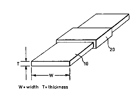
Figure 1 shows an embodiment of an inductor according
to an aspect of the present invention. The conductor
comprises a conductor bar (10) surrounded by a sheath
(20). The conductor bar (10) has a width "W" and a
thickness "T".
The advantages provided by the geometry of the inductor
of figure 1 will be better understood by considering
the analysis given below of the conductors shown in
figures 2 and 3. Figure 2 shows a cylindrical
conductor of length "L" and diameter "D", whilst figure
3 shows a generally rectangular conductor of length
CA 02268716 1999-04-15
WO 98119318 PCTIGB97102937
12
"L", width "W" and thickness "T".
For a circular conductor of length "L" and diameter "D"
nD Z
Cross Sectional Area (CSA) of conductor =
4
Circumference of conductor = nD
Surface Area (SA) of conductor = nD x L
where ~c - 3.142
D = conductor diameter
L = conductor length
n
for D = 1 unit, the CSA = ~ Sq.units or
units 4 4
the circumference = z
The SA = ~cL
For a rectangular strip conductor of width "W"
thickness "T" and length "L"
Cross Sectional Area (CSA) of conductor = W x T
Circumference of conductor = 2[W+T]
Surface Area (SA) of conductor = 2L[W+T]
35
for a rectangular strip conductor with a CSA of ~ sq
n 4
units we have W x T= -
4
and 2[W+T] - circumference of bar.
The circumference is a minimum when W=T i.e. bar has
square cross-section and circumference = 4W=4T
and Wz
4
Therefore the circumference of the bar = 4x'~=2 r
2
which is greater than '~ . Hence the circumference of a
square bar is greater than the circumference of a
circular bar for a fixed CSA.
CA 02268716 1999-04-15
WO 98119318 PCTIGB97102937
13
Then in general for a constant CSA as W
T ~ 0 or as T -- ~, W ~ 0. Therefore 2 [W+T) is always
greater than n .
Therefore the circumference of a rectangular bar is
always greater than the circumference of a circular bar
for equal CSAs.
It therefore follows that for a given CSA of circular
conductor, a rectangular conductor with the same CSA
will have a greater circumference, which approaches
infinity as its thickness becomes very small.
It further follows that if the above conductors each
have length "L" units then the surface area of the
rectangular strip conductor will also approach infinity
as its thickness becomes very small.
These dimensional relationships between circular and
rectangular conductors have considerable significance
in conductor designs) as the following properties
apply:-
- 1. At ultra low frequencies [d.c (OHz) to about
100Hz] electric currents propagate almost equally
throughout the CSA of a conductor.
2. At higher frequencies (above 100Hz) electric
currents tend to migrate towards the outer
surfaces of a conductor. This effect is termed
the "skin effect" of the conductor. The changes
imposed by the skin effect will be less in a
rectangular type of conductor when compared with a
circular conductor of the same CSA. A rectangular
conductor made of the same material and of the
same CSA will therefore have a much increased high
frequency current carrying capability.
. ~ ,
CA 02268716 1999-04-15
WO 98/19318 PCTIGB97102937
19
3. As electric currents are passed through a
conductor the reactance of that conductor creates
a heating effect within the conductor which
effectively limits the maximum current which it
might carry. For any given CSA of conductor the
rectangular type of conductor can be designed such
that the ratio of thickness to width gives a much
greater surface area and hence cooling capability
than its circular equivalent.
For all of these reasons, use of a rectangular
conductor is an improvement on the use of a circular
conductor.
The inductance of a coil of wire may be increased by
forming the coil around a core of suitable material
with which to concentrate the lines of magnetic flux.
For example, iron, brass and various grades of ferrite
may be used as material for the core. The conductor
may also be sleeved with these types of material i.e.
wholly or partially surrounded by a sJ_eeve.
If a rectangular type conductor is sleeved with, say,
ferrite, as shown in Figure 1, then its inductive
reactance will be greatly increased at high frequencies
and yet have little or no change at ultra-low
frequencies i.e. d.c. (OHz) to approx. 100Hz.
Therefore, when such rectangular sleeved inductors are
incorporated in high, low and bandpass filter designs
(such as these utilised in the design of High Frequency
Conditioned Power Network (HFCPN) directional couplers
- conditioning units) and in the provision of low and
high pass filter elements for high frequency
conditioned power networks, the problems associated
with IZR losses (conductor heat losses) and the
relatively large physical size of inductors may be
reduced or overcome.
_..~.....
CA 02268716 1999-04-15
WO 98119318 PCTIGB97/02937
At ultra-low frequencies i.e. up to say 100Hz
(electricity distribution networks are typically 50 or
60Hz and may also be direct current i.e. OHz), the
ferrite sleeve has negligible effect on the rectangular
5 conductor's performance. However, at frequencies above
lMHz the sleeve has a pronounced effect giving a
relatively high inductive reactance value and when
interconnected to suitable decoupling capacitance
produces high attenuation to the high frequency
10 signals.
Conventional inductors suffer a problem at high
frequencies due to their interwinding capacitance i.e.
the capacitance offered by each turn to the next. By
15 utilising a rectangular sleeved reactance type of
inductor this interwinding capacitance effect is
minimised. The reactive sleeving material may be coated
onto the conductor over an insulative membrane if
required or included in a suitable adhesive resin
compound and formed over the conductor.
Heat dissipation may also be improved in this way and
the sleeving technique may be included in power cable
joints in order to develop high frequency directional
coupling within the joint housing (400) as illustrated
in Figure 4 for joining two polyphase cables (402,
410). Figure 5 illustrates the equivalent electrical
circuit diagram which has a directional coupling effect
at high frequencies.
Optimum coupling is from polyphase cable (402) to/from
single phase cable (404) via connector (406) with
minimal coupling to cable (402) due to the series
inductors Llo, LZo and L3o produced by the ferrite
sleeves (408) as shown in Figure 4. The cable phase
conductors may be of any cross section e.g. circular,
wedge shaped, square or rectangular, and are provided
with ferrite sleeves either on each conductor or formed
i n
CA 02268716 1999-04-15
WO 98119318 PCT/GB97I02937
16
over the bunched conductors. They may have rectangular
sections formed at the sleeves to produce optimum
performance as previously described.
Such sleeved inductive components may be included in
electrical network joints as shown in figure 4 (and
schematically in figure 5), or mounted inside equipment
such as transformers and switchgear housings, in
electricity meter housings or in electrical appliances.
Indeed electricity meter current coils may be sleeved
such that their reactance increases with frequency and
may form part of an integral filter or high frequency
directional coupler or HFCPN ~~conditioning unit".
Similarly, fuse elements may be sleeved and have
elements formed from rectangular section conductors in
order that their inductive reactance might increase
with frequency and that they might form part of a
directional coupler or HFCPN conditioning unit.
It might be that a sufficient inductive reactance
values) might be obtained, at high frequencies, in
certain items of electrical plant such as cables,
- meters, switchgear and transformer bushings by
retrofitting suitable ferrite sleeves over existing
conductor sections (e.g round, ecliptical, polysided,
rectangular, square or triangular etc). This is
illustrated Figure 6. The preferable solution is for a
rectangular section of a similar area to be suitably
sleeved with ferrite or other similar material.
Figure 13 shows a three core cable 1300, around the
cores of which is fitted a sleeve 1320 according to the
present invention in order to form an inductive
element. The sleeves could of course be '~retro-fitted"
to an already laid conductor cable and also not all of
the conductors need to be fitted with sleeves.
Furthermore, the cable could of course include more or
... ? -__....
CA 02268716 1999-04-15
WO 98119318 PCTIGB97102937
17
less than three conductors.
The cable 1300 comprises an outer cable sheath 1330
inside which is a neutral earth sheath 1340.
Surrounding the three conductors 1310 is a layer of
insulative filler 1350 which keeps the conductors away
from the neutral earth sheath 1340. Each of the
conductors are covered by respective separate
insulative sheaths 1360 and all three conductors are
surrounded by a single sleeve 1320 according to the
present invention.
The sleeve 1320 contains a quantity of ferromagnetic
material which is chosen to be proportional to the
vector sum of the 50/60Hz current in the polyphase
conductors 1310. The properties of the material affect
the quantities utilised or required. The sleeve may be
split to facilitate its ease of fitting (i.e. ensuring
that there is no need to cut the conductors) and may be
held in place by a non-metallic clamp or "P"-clip 1370.
The value of inductance produced by this arrangement
will depend on the type or grade of ferromagnetic
material used, its overall length and its proximity to
the conductors: The greater the thickness of the
ferromagnetic sleeve the less likely it is that it will
saturate due to the 50/60Hz vector sum of the polyphase
current in the conductors.
A suitable material for the sheath could be Neosid MMG
ferrite grade F9C. For a sleeve having dimensions, for
example, of external diameter 63 mm, internal diameter
38mm and thickness 25mm, the magnitude of the vector
sum of the current flowing in one direction through the
ferrite is approximately 25 amps when saturation begins
to occur. Saturation current can be increased by
fitting a thicker sleeve with the same internal
diameter. In this example, the arrangement produces an
inductance of 11 ,uH per 25mm of length. Inductance can
CA 02268716 1999-04-15
WO 98119318 PCT/GB97/02937
18
be increased by increasing the length of the ferrite
and this increase is linear i.e. a 50mm length giving
22,uH etc .
The basic elements of a network conditioning unit 1104
according to one aspect of the present invention are
illustrated in Figs. lla and llb. Fig. lla shows a
conditioning unit 1104 (as also designated 1000 in fig.
10). The conditioning unit can be considered to be
equivalent to a low pass filter 1100 and a coupling
capacitor element 1102 (which can be considered to be a
high pass filter element).
The low pass filter element 1100 allows mains power to
be supplied from the distribution network to a consumer
whilst preventing high frequency communication signals
from entering the consumers premises. A coupling
capacitor, or high pass filter element, 1102 is
provided to couple the high frequency communication
signals onto the distribution network whilst preventing
the mains power from entering the communications
apparatus.
The conditioning unit components may be fitted into e.g
an electricity meter case located in a consumer's
premises, or possibly may be set into a compartment at
the rear of such a meter. Alternatively the necessary
components may be located in e.g. a customer's high
rupturing capacity (HRC) fuse or cut-out unit.
Referring to Fig. 12, an embodiment of a conditioning
unit (essentially a filter) according to an aspect of
the invention is indicated generally by the reference
numeral 1200 and is connected between a mains
electricity input 1202 and a mains electricity output
1204. A signal input/output line 1206 is also
connected into the filter. The mains power line is a
standard 50Hz or 60Hz mains electricity power supply
providing a domestic electricity power source of 110v
or 240v at a maximum current of 100 amps for normal
usage.
CA 02268716 1999-04-15
WO 98119318 PCT/GB97102937
19
The filter 1200 may be assembled into a shielded box
which prevents radiation of the communication signals
to externally located appliances and which provides a
connection 1208 to earth for the signal input/output
line 1206. The filter 1200 includes a first or main
inductor 1210 according to an aspect of the present
invention. This provides an inductance of
approximately 50~H. This may be a minimum for the
signal characteristics utilised, or possibly an
inductor of 10~H or less would suffice. The use of
different materials or a plurality of series inductors
may increase the inductance of the inductor up to, for
example, approximately 200~.H.
An end of the main inductor 1210 is provided with a
connection to the signal input/output line 1206. A
first connection 1212 between the mains electricity
input 1202 and signal input/output line 1206 comprises
a first or coupling capacitor 1214 having a
capacitance of between 0.01 and 0.50~.F, and preferably
around 0.1~,F. This coupling capacitor 1214 is
connected to a first fuse 1216 which is arranged to
blow in the event of failure or a fault developing in
capacitor 1214.
A second connection 1218 includes a second capacitor
1220 having a capacitance of between 0.001 and 0.50~F,
preferably around 0.1~.F. This capacitor provides
further attenuation of the communication signals by
shorting to the earth or ground 1208. A second fuse
1222 is provided to blow if a fault develops in the
second capacitor 1220, thereby preventing further unit
damage. w
The signal input/output line 1206 is connected to a
second inductor 1224 which may be constructed in
accordance with the present invention and having an
inductance of approximately 250~H minimum. This
inductor is provided as a damage limiter in the event
of failure of the coupling capacitor 1204. In the
event of such failure this inductor provides a path to
i n
CA 02268716 1999-04-15
WO 98/19318 PCT/GB97/02937
the ground 1208 for the 50Hz mains electricity power
frequency, thereby blowing fuse 1206. The inductor has
no effect on the communication frequency signals
present on the signal input/output line 1206.
5
Fig. 7 shows a circuit diagram of a second embodiment
of a filter according to an aspect of the present
invention. The filter 700 includes a pair of inductors
L1, L2 (which may be constructed in accordance with the
10 present invention) arranged in series between a mains
electricity input 720 and a mains electricity output
740. A preferred value for L1 and L2 is approximately
16~.H. L, and L2 may be of different values to reduce
harmonic response relationships. Connected between the
15 RF input line 760 and the mains input 720 is a first
fuse F1 and capacitor C1, and connected between the RF
input 760 and ground is a third inductor L3,(which may
also be constructed in accordance with the present
invention) which acts as an RF choke and has a typical
20 value of 250~.H.
Connected in a similar fashion between the connection
point of L1 and L2 and ground is a second fuse F2 and
second capacitor C2. Connected between the mains
electricity output 74 and ground is a third fuse F3 and
third capacitor C3. A typical value for the capacitors
is around 0.1~F and for the fuses approximately 5 amps
HRC (high rupturing capacity).
The values given for these components are exemplary
only, and different preferred values will be
appropriate for other design frequencies and
electricity network parameters.
Turning to Fig. 8 a typical housing arrangement for a
network conditioning unit according to an embodiment of
the present invention is shown. The main inductors L1
and L2 are housed within a shielding box 820. L1 and
L2 are shown as coil inductors, but could be replaced
by inductors according to the present invention.
Various connections are shown, including a
_._ _~__ ...._. r ~_.._ ...
CA 02268716 1999-04-15
WO 98/19318 PCT/GB97/02937
21
communication interface port 800 to which a user's
communication equipment would normally be connected.
However, as shown in Fig. 8, this port may be
terminated in an impedance matching port terminator
810.
Fig. 9 shows a circuit board 96 which fits inside the
unit 820 of figure 8 and houses the rest of the
circuitry for the network conditioning unit of figure
7. Connections A, B, C, D and E are shown which
connect to the appropriate points of the box shown in
figure 8.
Fig. 10 is a schematic representation of a network
conditioning unit 1000, showing the various building
blocks 1005-1060 of the network conditioning element.
To design a suitable network conditioning unit, the
circuits represented by blocks 1010 and 1060 should be
high-impedance elements over the required
communications frequency spectrum (eg. lMHz and above)
and low impedance elements at frequency of mains
electricity supply (ie. 50/60Hz) i.e. these elements
are inductors. Similarly blocks 1005 and 1020 should
be low impedance coupling elements over the required
communications frequency spectrum and high impedance
isolating elements at the frequency of the mains
electricity supply ie. they are capacitors.
HRC fault current limiting fusible safety links (1040
and 1050) are provided in series with elements 1005 and
1020. An additional impedance matching network 1030
may be included for connection to a communications
port. This element may be external to the network
conditioning unit 1000.
The optimum values of items 1010, 1005, 1020 and 1060
will be dependant upon factors including:-
a) The required frequency range over which the network
is to be conditioned.
CA 02268716 1999-04-15
WO 98/19318 PCT/GB97/02937
22
b) The unit length of the network which is to be
conditioned.
c) The number and types of loads which may be
encountered on the network.
d) The characteristic impedance of the network phase
conductors with respect to each other and/or earth (as
appropriate) i.e. conductor outer electrical sheath.
e) The impedance of the communications interface
devices.
The network conditioning unit may be filled with air,
inert gas, resin compound or oil depending upon the
location and load and/or fault current ratings of the
conditioning unit. Also it may be, for example, sited
indoors, pole mounted, buried underground or inserted
in street lamp columns.
Similarly items 1010 and 1060 may comprise a number of
individual inductors in series, and if no
interconnection is required, for example, on some
street lights, items 1040, 1005, 1030 and 1060 may be
omitted.
Items 1005 and 1020 may comprise of a number of
capacitors in series and/or parallel configuration
depending upon working voltages encountered ie. 240,
415, llkV, 33kV etc. Alternatively, or additionally,
items 80 and 82 may comprise of two or more capacitors
in parallel in order to overcome, for example,
deficiencies in-capacitor design when conditioning a
network over a relatively wide frequency range, for
example 50 MHz to 500 MHz.
Furthermore, items 1010, 1050 and 1020 of the network
conditioning unit may be cascaded if required. In a
typical design, the greater the number of cascaded
elements the sharper will be the roll-off response of
the filter and the greater its attenuation, subject to
T ..._. __.._ .. .
. ____~.__ _. . . .._.... . _. _ _. .
CA 02268716 1999-04-15
WO 98/19318 PCTIGB97/02937
23
avoidance of resonances etc.
The above embodiments of the present invention have
been described by way of example only and various
alternative features or modifications from what has
been specifically described and illustrated can be made
within the scope of the invention, as will be readily
apparent to a person skilled in the art.