Sélection de la langue

Search

Sommaire du brevet 2271033 

Énoncé de désistement de responsabilité concernant l'information provenant de tiers

Une partie des informations de ce site Web a été fournie par des sources externes. Le gouvernement du Canada n'assume aucune responsabilité concernant la précision, l'actualité ou la fiabilité des informations fournies par les sources externes. Les utilisateurs qui désirent employer cette information devraient consulter directement la source des informations. Le contenu fourni par les sources externes n'est pas assujetti aux exigences sur les langues officielles, la protection des renseignements personnels et l'accessibilité.

Disponibilité de l'Abrégé et des Revendications

L'apparition de différences dans le texte et l'image des Revendications et de l'Abrégé dépend du moment auquel le document est publié. Les textes des Revendications et de l'Abrégé sont affichés :

  • lorsque la demande peut être examinée par le public;
  • lorsque le brevet est émis (délivrance).
(12) Demande de brevet: (11) CA 2271033
(54) Titre français: DISPOSITIF DERIVEUR DE COURANT ELECTRIQUE
(54) Titre anglais: POWER DIVERTING DEVICE
Statut: Réputée abandonnée et au-delà du délai pour le rétablissement - en attente de la réponse à l’avis de communication rejetée
Données bibliographiques
(51) Classification internationale des brevets (CIB):
  • H04M 19/00 (2006.01)
(72) Inventeurs :
  • MALMGREN, CARL HENRIK JORGEN (Suède)
  • EMERICKS, ANDERS HARALD (Suède)
  • HELLBERG, HENRIK HELMER (Suède)
  • ISRAELSSON, MATTIAS (Suède)
(73) Titulaires :
  • TELEFONAKTIEBOLAGET LM ERICSSON
(71) Demandeurs :
  • TELEFONAKTIEBOLAGET LM ERICSSON (Suède)
(74) Agent: MARKS & CLERK
(74) Co-agent:
(45) Délivré:
(86) Date de dépôt PCT: 1997-11-07
(87) Mise à la disponibilité du public: 1998-05-22
Requête d'examen: 2002-09-09
Licence disponible: S.O.
Cédé au domaine public: S.O.
(25) Langue des documents déposés: Anglais

Traité de coopération en matière de brevets (PCT): Oui
(86) Numéro de la demande PCT: PCT/SE1997/001871
(87) Numéro de publication internationale PCT: SE1997001871
(85) Entrée nationale: 1999-05-07

(30) Données de priorité de la demande:
Numéro de la demande Pays / territoire Date
9604095-1 (Suède) 1996-11-08

Abrégés

Abrégé français

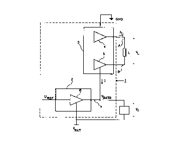
Cette invention concerne un procédé et un dispositif qui permettent de dériver le courant dans un circuit électrique (1), tel qu'un circuit d'abonné comprenant une transmission bifilaire équilibrée. Ce circuit comprend un utilisateur (3) qui a des besoins variables en matière de tension, ces besoins étant gérés en fonction de la caractéristique d'alimentation du dispositif et de la résistance dans la transmission bifilaire (A, B, L). Les besoins en tension de l'utilisateur sont renvoyés par l'intermédiaire d'un signal de référence (U¿REF?) à l'entrée d'un circuit régulateur de tension (2), lequel va envoyer à l'utilisateur une tension d'actionnement (V¿BAT2?) qui est fonction de la valeur du signal de référence. Le circuit régulateur de tension (2) reçoit une tension d'alimentation (V¿BAT?), la tension du régulateur (V¿0?) étant déterminée en calculant la différence entre la tension d'actionnement (V¿BAT2?) et la tension d'alimentation (V¿BAT?). Un dispositif externe (8), qui est monté en parallèle au circuit régulateur de tension et qui peut consister en une résistance, est connecté de manière à dériver toute puissance excédentaire générée dans le circuit régulateur de tension. Cette dérivation se fait à l'aide de la totalité ou d'une partie du courant d'alimentation de l'utilisateur qui est amené à la résistance externe, la totalité ou une partie de la puissance excédentaire y étant ensuite libérée.


Abrégé anglais


The present invention relates to a method and a device for diversion of power
in an electric circuit (1), e.g. a subscriber circuit with a balanced two-wire
transmission, comprising a user (3) with a variable voltage requirement, which
is controlled by the supply characteristic of the device and the resistance in
the two-wire transmission (A, B, L). The voltage requirement of the user is
fed back via a reference signal (UREF) to an input of a voltage-regulating
circuit (2), which supplies the user with a drive voltage (VBAT2) adapted to
the value of the reference signal. The voltage-regulating circuit (2) is fed
with a supply voltage (VBAT) and a regulator voltage (V0) is defined as the
difference between the drive voltage (VBAT2) and the supply voltage (VBAT).
Parallel with the voltage-regulating circuit, an external device (8), e.g. a
resistance, is connected in order to divert an undesired power generation in
the voltage-regulating circuit through the whole or part of the supply current
of the user being led to the external resistance and there the whole or part
of the power generation is emitted.

Revendications

Note : Les revendications sont présentées dans la langue officielle dans laquelle elles ont été soumises.


7
Claims
1. Method for diversion of power in an electric device comprising a user with
a varying voltage requirement, where a voltage-regulating circuit supplies the
user
with at least part of the current requirement (I) of the user and at least
part of the
drive voltage (V BAT2) of the user, which is regulated through at least one
reference
signal (U REF) from the user being fed back to the voltage-regulating circuit,
characterized in that an external device (8) comprising at least a resistive
part,
is connected in parallel with the above mentioned voltage-regulating circuit,
which
leads to the whole or a part of the current requirement (I) of the user
passing through
and being emitted as power in the external device.
2. Method according to Claim 1, characterized in that the external device is
selected to be a resistance.
3. Device for diversion of power in an electric device which comprises a user
with a
varying voltage requirement, a voltage-regulating circuit which supplies the
user
with at least part of the current requirement (I) of the user and at least
part of the
drive voltage (V BAT2) of the user and a reference signal (U REF) from the
user
which is fed back to the voltage-regulating circuit in order to regulate the
drive
voltage (V BAT2) of the user, characterized in that an external device (8)
comprising at least a resistive part is connected in parallel with the above
mentioned
voltage-regulating circuit (2), whereby the whole or part of the current
requirement
(I) of the user is arranged to pass through the external device (8) and there
be given
off as power.
4. Device according to Claim 3, characterized in that the user (3) and the
voltage-regulating circuit (2) are arranged in a semiconductor circuit.

8
5. Device according to Claim 3, characterized in that the external unit (8)
comprises a resistance.
6. Device according to Claim 5, characterized in that the user (3) and the
voltage-regulating circuit (2) are arranged in a semiconductor circuit.
7. Device according to any of Claims 3-6, characterized in that the electric
device
(1) is a subscriber line circuit.

Description

Note : Les descriptions sont présentées dans la langue officielle dans laquelle elles ont été soumises.


CA 02271033 1999-OS-07
WO 98121876 1 PCT/SE97101871
Power diverting device
TECHNICAL FIELD
The present invention relates to a method and a device for diverting waste
power
in an electric device.
S
STATE OF THE ART
When connecting for example an electric circuit with a variable load, problems
can occur with overheating of certain of the constituent components in the
electric
circuit. This problem is known and a number of technical solutions have been
developed in order to take care of this.
In many solutions it is accepted that waste power occurs in the circuit. Other
solutions use a DC/DC-converter for each load, the output voltage of which is
continually controlled in order to be adapted according to the actual load.
Another
alternative is, if there is access to two or more supply voltages in the
circuit, to
reduce the waste power in the circuit through switching between them for the
lowest adequate supply voltage for the occasion, which is described in SE
Patent
9403876-7.
US Patent 5 428 682 describes a technique for conducting away heat in a
telephone
circuit. This consists of two line supply amplifiers, one for each exiting
telephone
line, which outputs are connected to earth respectively the supply voltage by
a pair
of switches and two external resistances. The switches permit a pole reversal
of a
DC-supply to the telephone line. In the external resistances the undesired
heat can
be given off and the heat generation in the telephone circuit remains at an
acceptable
level.

CA 02271033 1999-OS-07
WO 98/21876 PCT/SE97/01871
2
SE Patent 80034l9-2 describes a technique with connection of an external
resistance for heat diversion, which resembles greatly the technique in the
above
mentioned US Patent 5 428 682.
GB Patent 2 050 115 A describes a technique where a resistance is connected
into
the final stage of an amplifier which has a certain output line current. The
generated
power in the final stage transistors is reduced through a part of the output
line
current passing through the resistance, and in this way the generated heat in
the final
stage is held at an acceptable level.
FR Patent 2 690 S37 describes a technique where a current regulator in a line
supply
circuit limits an output current through the connection of a resistance.
DISCLOSURE OF THE INVENTION
1 S A circuit, for example a line circuit comprising a final stage and a
voltage regulator,
which is to drive a balanced two-wire transmission with both an AC-signal and
a
DC-current, has a DC-supply characteristic which means that the line voltage
and
the DC-current is a function of a combined resistance in the line and load of
the
circuit. With the line open, the line is supplied with the maximal line
voltage at the
same time as the DC-current is zero, and furthermore the final stage of the
circuit
must have access to a drive voltage which is somewhat greater than the
required line
voltage. The drive voltage is obtained from the output of the voltage
regulator which
in turn is supplied from the drive voltage of the circuit.
When the line is loaded the line voltage will drop and the DC-current will
rise
depending on the resistance of the line and the load and on the supply
characteristic
of the line circuit. A so-called regulator voltage, which is the difference
between the
supply voltage of the circuit and the drive voltage of the final stage, is
generated in
this case over the voltage regulator at the same time as the DC-current flows
through it, which leads to an undesirable power generation in the voltage
regulator.

CA 02271033 1999-OS-07
WO 98I21876 PCT/SE97/01871
3
The undesired power generation can be difficult to lead away so that the
temperature of the circuit is held at a safe level.
The power generation in the circuit, more closely defined that over the
voltage
S regulator, is greatest in short lines, i.e. when the total resistance of the
line and the
load has a low value, as both the regulator voltage and the DC-current through
the
voltage regulator are large.
The present invention tackles a problem with diverting waste power in a
circuit
IO through emitting it in an outer component.
Another problem is to obtain the above described function with the smallest
poss-
ible interference in an existing circuit.
15 The obj ect of the present invention is, through diverting a part of the
waste power
of a circuit to an outer component, to increase the life length of the circuit
and to
reduce its thermal effects.
The above problem is solved through connecting an external component, e.g. a
20 resistance, in parallel with the voltage regulator of the circuit, which
leads to that a11
or part of the waste power of the circuit being emitted in the external
component.
An electric device, e.g. a subscriber line circuit, comprises a user with a
variable
voltage requirement and a voltage-regulating circuit, e.g. a voltage
regulator. The
25 voltage requirement of the user is fed back via a reference signal to an
input on the
voltage regulator, which supplies the user with a drive voltage adapted to the
value
of the reference signal. Over the voltage regulator there is formed a voltage
drop
from the difference between the drive voltage and the supply voltage of the
circuit.
The size of the voltage drop depends on the value of the varying drive
voltage.
30 When the voltage regulator is connected in parallel with an external
component, e.g.

CA 02271033 1999-OS-07
WO 98I21876 PCT/SE97/01871
4
a resistance, the electric circuit is relieved when all or part of the user's
supply
current is led to the external resistance and then all or part of the waste
power of the
voltage regulator is emitted.
An advantage of the suggested invention is that only one resistance is
required in
order to take care of waste power in the circuit. Another advantage is that
there is no
longer need for any switches for pole reversing of the DC-supply of the two-
wire
transmission.
Yet another advantage is that the invention is easy to implement without large
changes to an already existing circuit solution.
The invention will now be described more closely with the help of the
preferred
embodiment and with reference to the appended drawing.
DESCRIPTION OF THE DRAWING
Figure 1 shows an electric circuit with a heat dissipating device according to
the
invention.
PREFERRED EMBODIMENT
Figure 1 shows a generalized view of an electric circuit 1 with a heat
dissipating
device 8 according to the invention. The electric circuit comprises a voltage-
regulating circuit 2, which is connected to the supply voltage VBAT of the
circuit
and which supplies a user 3 with a drive voltage VBAT2 ~ In the embodiment
shown
the user 3 is a schematically shown subscriber line circuit comprising two
final
amplifiers 4 and S with two wires A and B, which at their other end are
connected to
a load L in the form of e.g. a subscriber apparatus, and the voltage-
regulating circuit
comprises a voltage regulator 6. The user is connected between earth GND and
the
output 7 of the voltage regulator. A heat dissipating device 8, which
comprises at

CA 02271033 1999-OS-07
WO 98/21876 PCT/SE97/01871
least one component with a resistive part, e.g. a resistance, is connected
parallel
with the output 7 of the voltage regulator and the supply voltage VBAT
The user which is connected between earth GND and the drive voltage VgAT2 h~
5 a varying voltage requirement which can be read and fed back to the voltage
regulator 6 of the circuit via a reference signal UHF. Depending on the
voltage
requirement of~the user a voltage drop VO of varying size will occur between
the
drive voltage VBAT2 and the supply voltage VBAT of the circuit.
In the embodiment shown a current IL flows from one amplifier 4 through the
wire
A to the load L and further to the second amplifier 5. The wires A and B and
the
load L have an inbuilt resistance, which leads to the occurrence of a
potential differ-
ence VL between the amplifiers. Variations in the current and in the inbuilt
resist-
ance for the two-wire transmission result in a potential variation between the
amplifiers. The potential variation leads to the voltage requirement of the
user also
being variable and furthermore a variable supply current I flowing through the
user.
A voltage VO occurs over the voltage-regulated circuit 2, which is equal to
VO - VBAT - VBAT2 C1)
where the drive voltage is a function of the potential difference between the
final
amplifiers, VBAT2 - f ~VL)~ which gives
VO - VBAT - f ~VL) C2) .
From equation 2 it can be clearly seen that the regulator voltage VO can vary
de-
pending on the resistance in the line and the load. If the external power
dissipating
device 8 is not connected then the whole of the supply current I will flow
through
the voltage-regulating circuit 2 and give rise to the undesired power
generation
when the regulator voltage VO increases. When the external device 8 is turned
on,

CA 02271033 1999-OS-07
WO 98/21876 PCT/SE97/01871
6
all or part of the current I will pass through the external device 8 instead
of through
the voltage-regulating circuit 2. The undesired waste power will therefore be
emitted in the external device and not influence the thermal conditions for
the
electric circuit 1.
This method for dissipating the waste power in an electric device can be
applied in
the case that a part of a current I; which flows through a user with a
variable voltage
requirement, is fed from a voltage-regulating circuit 2. Through the
connection of an
external device 8 with a resistive part, the whole or part of the current can
be led
away from the voltage-regulating circuit and away from the electric device.
The external power dissipating device can in its simplest embodiment consist
of a
resistance but it only needs to include a component with a resistive
characteristic,
e.g. a transistor, in order for the device to function according to a power
dissipating
principle.
A subscriber line circuit is often realized in a semiconductor chip, so-called
SLIC,
which has a limited durability as far as heat generation is concerned. The
above
described embodiment is naturally applicable even in the.case when for example
the
user and the voltage-regulating circuit are not constructed on the same semi-
conductor chip, but the dashed line can for example be a printed circuit or an
electric device where a heat dissipating function is desired in the form of a
device 8.
The invention is naturally not limited to the embodiments described above and
shown on the drawing but can be modified within the scope of the accompanying
claims.

Dessin représentatif
Une figure unique qui représente un dessin illustrant l'invention.
États administratifs

2024-08-01 : Dans le cadre de la transition vers les Brevets de nouvelle génération (BNG), la base de données sur les brevets canadiens (BDBC) contient désormais un Historique d'événement plus détaillé, qui reproduit le Journal des événements de notre nouvelle solution interne.

Veuillez noter que les événements débutant par « Inactive : » se réfèrent à des événements qui ne sont plus utilisés dans notre nouvelle solution interne.

Pour une meilleure compréhension de l'état de la demande ou brevet qui figure sur cette page, la rubrique Mise en garde , et les descriptions de Brevet , Historique d'événement , Taxes périodiques et Historique des paiements devraient être consultées.

Historique d'événement

Description Date
Le délai pour l'annulation est expiré 2004-11-08
Demande non rétablie avant l'échéance 2004-11-08
Réputée abandonnée - omission de répondre à un avis sur les taxes pour le maintien en état 2003-11-07
Lettre envoyée 2002-10-16
Requête d'examen reçue 2002-09-09
Exigences pour une requête d'examen - jugée conforme 2002-09-09
Toutes les exigences pour l'examen - jugée conforme 2002-09-09
Lettre envoyée 1999-10-22
Inactive : Page couverture publiée 1999-10-07
Inactive : Transfert individuel 1999-09-28
Inactive : CIB en 1re position 1999-06-23
Inactive : Notice - Entrée phase nat. - Pas de RE 1999-06-08
Inactive : Lettre de courtoisie - Preuve 1999-06-08
Demande reçue - PCT 1999-06-04
Demande publiée (accessible au public) 1998-05-22

Historique d'abandonnement

Date d'abandonnement Raison Date de rétablissement
2003-11-07

Taxes périodiques

Le dernier paiement a été reçu le 2002-10-31

Avis : Si le paiement en totalité n'a pas été reçu au plus tard à la date indiquée, une taxe supplémentaire peut être imposée, soit une des taxes suivantes :

  • taxe de rétablissement ;
  • taxe pour paiement en souffrance ; ou
  • taxe additionnelle pour le renversement d'une péremption réputée.

Les taxes sur les brevets sont ajustées au 1er janvier de chaque année. Les montants ci-dessus sont les montants actuels s'ils sont reçus au plus tard le 31 décembre de l'année en cours.
Veuillez vous référer à la page web des taxes sur les brevets de l'OPIC pour voir tous les montants actuels des taxes.

Historique des taxes

Type de taxes Anniversaire Échéance Date payée
Taxe nationale de base - générale 1999-05-07
Enregistrement d'un document 1999-09-28
TM (demande, 2e anniv.) - générale 02 1999-11-08 1999-11-01
TM (demande, 3e anniv.) - générale 03 2000-11-07 2000-11-01
TM (demande, 4e anniv.) - générale 04 2001-11-07 2001-10-23
Requête d'examen - générale 2002-09-09
TM (demande, 5e anniv.) - générale 05 2002-11-07 2002-10-31
Titulaires au dossier

Les titulaires actuels et antérieures au dossier sont affichés en ordre alphabétique.

Titulaires actuels au dossier
TELEFONAKTIEBOLAGET LM ERICSSON
Titulaires antérieures au dossier
ANDERS HARALD EMERICKS
CARL HENRIK JORGEN MALMGREN
HENRIK HELMER HELLBERG
MATTIAS ISRAELSSON
Les propriétaires antérieurs qui ne figurent pas dans la liste des « Propriétaires au dossier » apparaîtront dans d'autres documents au dossier.
Documents

Pour visionner les fichiers sélectionnés, entrer le code reCAPTCHA :


Pour visualiser une image, cliquer sur un lien dans la colonne description du document. Pour télécharger l'image (les images), cliquer l'une ou plusieurs cases à cocher dans la première colonne et ensuite cliquer sur le bouton "Télécharger sélection en format PDF (archive Zip)" ou le bouton "Télécharger sélection (en un fichier PDF fusionné)".

Liste des documents de brevet publiés et non publiés sur la BDBC .

Si vous avez des difficultés à accéder au contenu, veuillez communiquer avec le Centre de services à la clientèle au 1-866-997-1936, ou envoyer un courriel au Centre de service à la clientèle de l'OPIC.


Description du
Document 
Date
(aaaa-mm-jj) 
Nombre de pages   Taille de l'image (Ko) 
Dessin représentatif 1999-08-26 1 4
Description 1999-05-06 6 263
Revendications 1999-05-06 2 56
Abrégé 1999-05-06 1 60
Dessins 1999-05-06 1 12
Rappel de taxe de maintien due 1999-07-07 1 112
Avis d'entree dans la phase nationale 1999-06-07 1 194
Courtoisie - Certificat d'enregistrement (document(s) connexe(s)) 1999-10-21 1 115
Rappel - requête d'examen 2002-07-08 1 128
Accusé de réception de la requête d'examen 2002-10-15 1 176
Courtoisie - Lettre d'abandon (taxe de maintien en état) 2004-01-04 1 177
PCT 1999-05-06 9 353
Correspondance 1999-06-07 1 30