Note : Les descriptions sont présentées dans la langue officielle dans laquelle elles ont été soumises.
CA 02272104 2007-10-09
64,159-1618
-1-
METHOD FOR MAKING A THIN FYLM RESONANT
MICROBEAM ABSOLUTE PRESSURE SENSOR
BACKGROUND OF THE INVENTION
The invention pertains to sensors and particularly to resonant sensors. More
particularly, the invention pertains to resonant microbeam pressure sensors
having a
polysilicon microbeam resonator formed from a portion of the sensor diaphragm.
Previous developments have resulted in surface micromachined pressure sensors
each of which had a pressure diaphragm formed from a deposited thin film of
polysilicon with an integral vacuum cavity reference directlv under the
diaphragm.
Deformations of the diaphragm with applied pressure caused shifts in a
Wheatstone
bridge fabricated from polysilicon piezoresistors deposited on the diaphragm
resulting
in a voltage output indicating the amount of pressure sensed bv the sensor.
The
Wheatstone bridge has a relatively low sensitivity to strain in the diaphragm,
and the
output voltage requires an analog-.to-digital (A/D) conversion to be used in
digital
systems.
Several patents provide background to the present description. U.S. patent #
4,744,863, by inventors Henry Guckel and David W. Bums. issued Mav 17. 1988,
and
entitled "Sealed cavitv semiconductor pressure transducers and method of
producing the
same:" U.S. Patent # 5,417,115, by inventor David W. Burns. issued Mav 23.
1995. and
entitled "Dielectricallv isolated resonant microsensors;" U.S. Patent #
5,458,000, by
inventors David W. Burns and J. David Zook, issued October 17, 1995, and
entitled
"Static pressure compensation of resonant integrated microbeam sensors;" and
U.S.
Patent # 5,511,427, by inventor David W. Bums, issued April 30, 1996, and
entitled
"Cantilevered microbeam temperature sensor"'.
European Patent Application 91302715.7 discloses polysilicon resonating beam
transducers and a method for making them. U.S. Patent 5,417,115 discloses
dielectrically
isolated resonant microsensors and a method for making them.
SUMMARY OF THE INVENTION
The present invention has an integral vacuum cavity reference and a
polysilicon
diaphragm, but has a polysilicon resonator integrally formed from a portion of
the
diaphragm, thus being able to provide a frequency output that is a direct
measure of the
pressure applied to the top surface of the diaphragm, thus eliminating the
errors of the
RC \\ 1'. 1' ~a l S3i l l J +l'J iS:.{ "i4:t;!=l 1_i', =:/
CA 02272104 1999-05-18
a 4 /. w = ,
(insert as the last paragraph of >~A~~G~O~73~1D t~F THE ~IE; c~~T o:c page 1.)
European Patent Application 91302715,7 discloses po4Ysilicon resonating benrn
taanssiucers and a method for making them. U.S. Patent 5,417,115 discloses
dielr..ctrically isolated
resonant n3icrosensors and a rnethod for makir.g them.
AMENDED SHEET
TOIPL. F.0b
CA 02272104 2007-10-09
64159-1618
_~-
Wheatstone or other parameter transforming device deposited on the diaphragm
which
introduces errors into the results of the measured parameter. The output of
the present
micromachined sensor interfaces readily with digital and optical systems. The
invention
is a thin film resonant microbeam absolute pressure sensor that achieves the
advantageous objectives of having an integral vacuum reference, a frequency
output,
high sensitivity and integral stress isolation. Fabrication of this microbeam
sensor
requires no backside wafer processing, involves a process and layout
independent of
wafer thickness, can use full thickness die for high yield and robustness, and
the process
is compatible with a family of resonant sensors (including temperature and
strain).
The invention is a microstructure having a thin film diaphragm, at least one
embedded resonator, and an integral vacuum reference. The diaphragm and
resonator
are formed from polysilicon. This sensor may utilize a sensing and driving
mechanism
that is either electrical or optical, or a combination of electrical and
optical. The sensor
may have a single resonant microbeam or a multiple of microbeams which may
include
push-pull operation for temperature cancellation or compensation.
For more precise sensing, the microbeam sensor may incorporate integral stress
isolation using cantilevered single crystal silicon paddles. The sensor may be
configured into a differential pressure sensor by a process that uses
additional
micromachining while retaining the resonator in its own vacuum reference.
CA 02272104 2007-10-09
64159-1618
, =
-2a-
In accordance with this invention, there is provided
a method for making a thin film resonant microbeam absolute
pressure sensor, comprising: forming a first layer on a
substrate to define a first cavity; forming a second layer on
the first layer to define a channel; forming a third layer on
the second layer; removing portions of the third layer to form
a microbeam; forming a fourth layer on the third layer to
define a second cavity; forming a fifth layer on the fourth
layer; removing the second layer to form a channel to the
first and fourth layers; and removing the first and fourth
layers via the channel to result in the first and second
cavities proximate to the microbeam; and characterized in
that: the first, second and fourth layers comprise low
temperature oxide.
BRIEF DESCRIPTION OF THE DRAWING
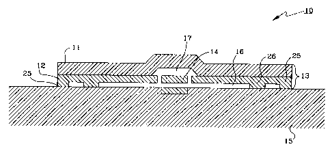
Figure 1 shows a resonant microbeam pressure sensor.
Figures 2a, 2b, 2c and 2d illustrate the stress
effects on a pressure sensing diaphragm.
Figure 3 is a schematic of a resonant microbeam
sensor diaphragm.
Figures 4a, 4b, 4c, 4d, 4e, 4f, 4g and 4h show a
process for fabricating a resonant microbeam sensor.
Figure 5 reveals an optically driven resonant
microbeam sensor.
Figure 6 illustrates an electrically driven resonant
microbeam sensor having an electrostatic drive line and a
piezoresistive sense line.
Figures 7a, 7b, 8a and 8b show single and multiple
resonator configurations, respectively.
CA 02272104 1999-05-17
WO 98/29722 PCT/US97/24108
-3-
Figures 9a and 9b reveal a stress isolating mounting for a resonant microbeam
sensor.
Figures 10a. l Ob and I Oc illustrate a resonant microbeam sensor having a
fiber
optic drive and sense mechanism.
. 5 Figures l la and l lb show a recessed stress isolating mounting for a
microbeam
sensor.
DESCRIPTION OF PREFERRED EMBODIMENTS
Figure 1 shows a cross-section of the present thin film resonant microbeam
absolute pressure sensor 10. Two lavers 11 and 12 of fine-grained polvsilicon
form
pressure sensitive diaphragm 13, with a resonant member 14 formed in lower
layer 12.
Composite diaphragm 13 is fabricated on a silicon substrate 15. Using surface
micromachining techniques. sacrificial oxides and reactive sealing, a vacuum
cavity
reference 16 is formed in the region between diaphragm 13 and substrate 15.
Pressure
applied to the topside of diaphragm 13 creates deformations into lower cavity
region 16,
stretching resonant microbeam 14 and causing shifts in its resonant frequency.
Microbeam 14 is free to vibrate into lower cavitv region 16 and into an upper
cavity
region 17 (also in vacuum). Optical or electrical drive mechanisms excite the
microbeam into resonance and detection of the vibration provides a quasi-
digital output
signal which is a measure of applied pressure. Multiple resonators can be
configured on
a single diaphragm 13 to provide compensation for temperature and common mode
effects. Diaphragm 13 can be circular or square; similarly, so can the die. An
optional
fabrication sequence using B:Ge codoped material provides significant stress
isolation
by undercutting silicon substrate 15 directly beneath the pressure sensor.
Other
micromachining steps can adapt resonant pressure sensor 10 to differential
pressure
sensor sensing applications using multiple devices or bv configuring an
additional
pressure port.
This device has a pressure diaphragm formed from a deposited thin film of
polysilicon. with an integral vacuum reference directly underneath the
diaphragm.
Deformations of the diaphragm with applied pressure caused resistance shifts
of a
Wheatstone bridge, fabricated from polysilicon piezoresistors deposited on the
diaphragm. Device 10 described here has an integral vacuum cavity 16 reference
and a.
CA 02272104 1999-05-17
WO 98/29722 PCT/US97/24108
-4-
polysilicon diaphragm 13, but has a polysilicon resonator 14 integrally formed
from a
portion of diaphragm 13, thus providing a frequency output that is a direct
measure of
pressure applied to the top surface of diaphragm 13 (see Figure 1) which
interfaces
readily with digital and optical systems.
Operation of device 10 can be noted by inspecting the illustrations in Figures
2a, 2b. 2c and 2d. Deformations of pressure-sensitive diaphragm 13 with
applied pressure
(PaPp) creates stress (an,.) in the plane of diaphragm 13 which increases
linearly with
pressure, for small deflections as shown by curve 18 in Figure 2b. The stress
6 and
strain s distributions in the plane of diaphragm 13, however, vary for points
near the
edge of diaphragm 13 or near the center. The stress (or strain) distribution
at the bottom
of diaphragm 13 is tensile near the center and compressive near the periphery.
Figure 2c shows stress and strain distributions of a diaphragm 13 based
pressure
sensor 10. A fully supported diaphragm 13 of radius 19 (h) and thickness 20 is
shown
in Figure 2a with pressure applied to the topside. The maximum tensile stress
occurs at
the diaphragm 13 edge, and increases linearly with applied pressure (in figure
2b). The
stress distribution at the bottom of the diaphragm 13 varies, according to
curve 22 of
figure 2c, from a tensile stress at the center to a compressive stress at the
periphery,
indicating that a resonator 14 is appropriately placed either at the diaphragm
13 center,
or at the periphery. Figure 2d shows the stress and strain profile 23 with
diaphragm 13
thickness 20, with a compressive stress at the upper surface and a tensile
stress at the
lower surface.
Resonant pressure sensors have been designed and fabricated with resonant
microbeams fabricated on single crystal silicon diaphragms. Smaller size,
large signal
and an integral vacuum reference 16 is obtained by the methods and innovation
described here. The single crystal silicon diaphragm is replaced with a much
smaller
(100 to 500 micrometers) polysilicon diaphragm 13, varying from 1.0 to 5.0
micron
thick. Diaphragm 13 is formed from two layers 11 and 12 of polysilicon, as
shown in
Figure 3. Resonator 14 is formed by etching two slits 24 in lower (beam)
polysilicon
layer 12. Upper (shell) polysilicon layer 11 increases diaphragm 13 thickness
and
contains a small cavity 17 directly above microbeam 14 to allow it to vibrate
unencumbered. Vacuum reference cavity 16 is located underneath lower
polysilicon
layer 12. Anchor regions 25 and 26, shown in Figures 1, 5 and 6, allow
diaphragm 13
CA 02272104 1999-05-17
WO 98/29722 PCT/US97/24108
-5-
to replicate as closely as possible clamped boundary conditions at the
periphery. These
consist of relatively wide anchor regions 25 for the outside of the plate, and
segmented,
narrow inner regions 26 for firming the displacements at the periphery.
The number of masking levels required for resonant absolute pressure sensor 10
= 5 is six: lower cavity masking level, lower drive, channel, beam, upper
cavity and shell.
Additional levels are required to form paddle-style stress isolation
(described below)
and piezoresistive or capacitive sense.
The lower cavity mask forms region 16 for the vacuum reference and allows
mechanical contact between the periphery of diaphragm 13 and underlying
substrate 15
through the lower cavity sacrificial oxide. The lower drive level is used to
form
photodiodes 31 in substrate 15 directly beneath microbeam 14. The photodiodes
will
create an electric field due to the photovoltaic effect when stimulated by
incident
radiation and allow optical interrogation of microbeam frequencies. This layer
can
similarly be used to form drive or sense electrodes in substrate 15 for
electrical versions.
The channel layer is used to provide access 60 for liquid access of etchant to
the upper
and lower cavities for removal of the sacrificial material. The channels are
required to
be thin for sealing purposes. The beam layer is used to define resonators. The
upper
cavity layer is used to pattern the upper cavity oxide immediately above
resonators 14.
Shell layer defines diaphragm 13 and completes the vacuum enclosure for
microbeam
14. The upper cavity 17, beam 14 and shell thicknesses are chosen to intensity
modulate the sensing radiation for optical detection and excitation. An
optional trench
mask is used to define a U-shaped trench around three sides of the paddles for
stress
isolation.
The microbeam fabrication process (see Figures 4a, 4b, 4c, 4d, 4e, 4f, 4g and
4h)
contains three LTO deposition steps and two polysilicon deposition steps.
Three
implants are used; two of them are blanket implants. No thermal oxidations are
required
in this sequence. Silicon nitride is used for an antireflection coating and a
scratch
protection layer. Processing of optically resonant microbeams 14 begins with a
nominally 7500 angstrom deposition of LTO 27 (i.e., low temperature oxide) on
a
silicon wafer 28 in figure 4a. Wafers 28 are n- or p-type with (optional)
inclusion of an
epitaxial layer on top of a codoped B:Ge etch stop layer. LTO 27 is patterned
and
etched using the lower cavity masking level to anchor diaphragm 13 to
substrate 15 and
CA 02272104 1999-05-17
WO 98/29722 PCTIUS97/24108
-6-
define the vacuum cavity reference region. An implant 29 is done through oxide
27
with a PR mask 30 of the lower drive layer to form p-n junctions 31 in
substrate 28 of
figure 4b. A thin, nominally 800 angstrom LTO layer is deposited and patterned
with the channel layer to form etch channels 60 to and through the anchor
regions 25 and 26
of figure 4c. A beam polysilicon layer 12 is deposited next, followed by an
implant,
patterning and etching to define beams 14 and remove beam polysilicon layer 12
in the
region between beam polysilicon layer 12 and beam 14 as shown in figure 4d.
The
thickness of beam polysilicon layer 12 is targeted at nominally 1.0
micrometer. A
nominally 7500 angstrom LTO layer 32 is deposited conformally over microbeam
14 in
figure 4e. The LTO is patterned with the upper cavity layer and etched to form
cavity
region 17 around the microbeam 14. A thicker shell polysilicon layer 11 (at
1.0 to 4.0
micrometers) is deposited and implanted in figure 4f, followed by an
intermediate
temperature anneal to set the strain field and drive the implant. Shell
polysilicon layer
11 and beam polysilicon layer 12 are then pattemed and etched using the shell
layer to
form diaphragm 13. A sacrificial etch is applied to remove LTO 27 and 32
thereby
resulting in cavities 16 and 17, as shown in figure 4g. Sacrificial etching 34
is done
using 1:1 HF:HCI, followed by withdrawal and the latest sublimation
techniques. A
thin layer of LTO is deposited followed by a 1600 angstrom layer of
polysilicon to seal
in a vacuum and form the reactive seal. Alternatively, silicon nitride may be
used for
sealing, or a polysilicon seal with the oxide omitted. A nominally 1000
angstrom thick
passivation layer 33 of silicon nitride is deposited. to enhance the seal and
performing
an additional function as an antireflection coating.
Stress isolation can be added by forming paddles upon which the absolute
pressure sensor is located. A layer of LTO is deposited, patterned and etched
with the
trench layer, followed by etching of the silicon nitride layer and silicon
through the
epitaxial layer. An additional layer of LTO is deposited for sidewall
passivation during
anisotropic etching. The LTO is blanket etched from the top side, leaving
oxide on the
exposed sides of the n-epitaxial layer. After anisotropic etching in EDP, the
LTO
passivation layers are removed.
Optical methods may be used to drive and sense the oscillations of a resonant
microbeam 14 using an optical fiber 36. Figure 5 shows an optically
driven/sensed thin
film resonant absolute pressure sensor. Light 35 from optical fiber 36 is
trained on
CA 02272104 1999-05-17
WO 98/29722 PCTIUS97/24108
-7-
resonator 14. A portion of light 35 is transmitted through shell layer 11 and
the beam
14 layer, striking an underlying photodiode 37. Light 35 generates an electric
field,
forcing microbeam 14 downward. Modulation of incident light 35 at the resonant
frequency excites beam 14, and results in a reflection of light 35 back
through fiber 36
which is also modulated and sensed externally with a photodiode. A second
method of
excitation uses the self-resonant approach and operates with continuous wave
incident
light 35.
Electrical drive/sense methods may be used to electrostatically excite the
microbeam and piezoresistively sense the deflections. Figure 6 shows an
electrostatic
drive line 38 and sensing piezoresistors with leadouts 40 for external
electrical
interconnection. Although single resonators 14 can be used to extract pressure
readings,
larger signals and a reduction in temperature sensitivity can be obtained
using multiple
resonators in a push-pull configuration. Cantilevered microbeam temperature
sensors
can be for temperature compensation. Figures 7a and 7b, and 8a and 8b show
single and
multiple resonator configurations, respectively. A single resonator 14 on a
circular
diaphragm 42 is shown schematically in figure 7a and on a square diaphragm 43
in
figure 7b. Multiple resonators 14. 41 and 44 on a circular diaphragm 42 are
shown
schematically in figure 8a and on a square diaphragm figure 8b.
Coupling to thin film resonators 14 using optical methods, for exaniple. can
induce undesirable packaging and mounting stresses on sensor 10, causing
baseline
shifts and hysteresis. A method for achieving stress isolation is to mount
sensing
devices 10 on a suspended paddle 45 of a substrate 28, in a side view of
Figure 9a,
which appreciably reduces the effects of detrimental stresses. Sensor 10 is
formed on
substrate 28 prior to formation of paddle 45.
Figure 9b shows top view of stress isolated resonant microbeam absolute
pressure sensor 10 on paddle 45 of substrate 28. The stress isolation results
from
positioning device 10 on a single crystal silicon paddle 45, suspended away
from the
mounting surfaces. Circular or square diaphragms can be mounted on paddle 45.
A
trench 52 parts three sides of paddle 45 from die 28. A square die 28 is
illustrated,
though it can also be circular.
A packaging configuration using an optical fiber 36 mounted to a silicon
pressure sensor 10 die 46 is illustrated in Figures 10a, l Ob and 10 c. An
optical fiber 36
CA 02272104 1999-05-17
WO 98/29722 PCT/US97/24108
-8-
is threaded through a glass or ceramic ferrule 47, which may have funnels on
one or
both ends. Ferrule 47 is attached to silicon die 46 which may be either square
or round.
A round die may be formed by using through-the-wafer etching techniques. A
cladding
48 surrounds optical fiber 36. Optical fiber 36 is used to drive and sense
microbeam 14.
Interface 49 provides for strain relief. A pressure port is cut into glass
ferrule 47 or
silicon die 46. Other sensor functions (temperature, strain, magnetic field,
and so forth)
can be measured using this packaging approach with alternate configurations.
A resonant microbeam absolute pressure sensor 10 may be situated on a circular
die 50. Side and top views of this configuration are shown in figures 11 a and
11 b,
respectively. Resonant pressure sensor 10 is built in a recess 51, to allow
connection to
a flat-faced ferrule 47 or cleaved fiber 36. Sensor 10 is on paddle 45 that is
suspended
apart from die 50 by trench 52. Dimensions 53 and 54 may be from 0.25 to 0.5
millimeter and from 0.5 to 2.5 millimeters, respectively.