Note : Les descriptions sont présentées dans la langue officielle dans laquelle elles ont été soumises.
CA 02273658 1999-06-07
1
METHOD AND APPARATUS FOR CANCELLING COMMON MODE NOISE IN
COMMUNICATIONS CHANNELS
DESCRIPTION
TECHNICAL FIELD:
This invention relates to noise cancellation and is especially applicable to
cancellation of common mode noise in communications channels, particularly
telephone
subscriber loops employing twisted-wire pairs.
BACKGROUND ART:
In theory, twisting together the conductors forming a twisted-wire cable, as
used
in a telephone subscriber loop, ensures that the impedance is balanced
throughout its
length. In practice, however, there are imbalances. For example, moisture
ingress
might cause one conductor to have greater leakage to ground, the twisting
might not be
uniform, and the conductors might be untwisted where taps are made. When a
signal
propagates along the cable, the waves on the respective conductors encounter
different
complex impedances. As a result, they may propagate at different speeds and be
subject
to different distortion. Upon arrival at the receiver, the two waves are no
longer
symmetrical. Although this effect can usually be ignored in conventional
telephone
systems, it presents problems in high speed digital subscriber loops,
especially Very
High speed Digital Subscriber Loops (VDSL) which operate at radio frequencies.
Radio-frequency (RF) signals from commercial AM or amateur radio stations
frequently
couple to twisted wire cables, particularly to overhead service drops, as a
common mode
noise signal. Because of the above-described cable imbalance, some portion of
such an
RF interference signal will usually convert to differential mode and be
coupled
inductively across the hybrid device. In addition, the stray capacitance
between the input
and output of the hybrid will couple the RF interference signal to appear at
the output
of the hybrid device. This may be significant if the RF interference signal is
relatively
large in amplitude.
Various systems have been proposed to cancel common mode noise in subscriber
loops. In T1E1.4/96-084 dated April 18, 1996, and at a VDSL workshop at IEEE
Globecom, November 18, 1996 in London, England, John Cioffi and John Bingham
proposed doing so by extracting a signal representing common mode noise and
filtering
it using an adaptive wide band filter to provide a radio frequency noise
estimate for
CA 02273658 1999-06-07
2
subtraction from the differential signal obtained from the secondary of the
hybrid
transformer. The coefficients of the adaptive filter were tuned during quiet
periods, i.e.
when no signal is being transmitted, to reduce the difference between the
differential
signal and the noise estimate signal substantially to zero. Unfortunately, the
adaptive
filter cannot readily compensate for the cross-coupling of the differential
signal and
common mode signals due to the loop imbalance and so, during signal
transmission, will
cancel part of the differential information signal too. Accordingly, the
resulting signal
supplied to the receiver will be distorted.
Canadian patent application No. 2,237,460 filed May 13, 1998, naming one of
the present inventors, disclosed a noise suppression circuit in which a noise
detection and
control unit scanned the operating band to identify noisy frequency bands and
suppressed
the noise in that band. The circuit is not entirely satisfactory because it
requires the
number of interfering RF signals to be few and does not cancel impulse noise.
Canadian
patent application No. 2,239,675 filed June 4, 1998, also naming such
inventor,
disclosed a wideband common mode noise canceller in which a digital common
mode
signal was filtered by an analysis filter bank to produce subband signals at
different
frequencies. Previous samples of each of the subband signals were summed and
compared with a predetermined noise threshold. If the summed noise signal was
greater
than the threshold, the subband signal was processed by a synthesis filter to
form a
component of a noise estimate signal for subtraction from the differential
signal. While
this circuit will compensate to some extent for stray capacitance of the
hybrid device and
the above-described loop imbalance caused by inductive coupling, its
performance is
limited.
DISCLOSURE OF INVENTION:
An object of embodiments of the present invention is to mitigate or eliminate
either or both of the above-described effects of impedance imbalance and
capacitive
coupling.
According to one aspect of the present invention, a noise cancellation circuit
for
a communications channel comprises a differential signal path and a common
mode
signal path connected to respective inputs of a summing device, the
differential signal
path comprising input means connected to the channel for receiving a
differential signal
therefrom and supplying the differential signal to a first of the inputs of
the summing
CA 02273658 1999-06-07
3
device, the common mode signal path comprising extraction means coupled to the
channel for extracting therefrom a common mode signal, means for generating a
common
mode noise estimate signal and applying said estimate signal to a second of
the inputs
of the summing device, coupling means for coupling at least part of the
extracted
common mode signal to an input of the generating means, the coupling means
having a
capacitive component equivalent to stray capacitance coupling between an input
and an
output, respectively, of the input means, the circuit further comprising means
for
compensating for phase differences between the differential signal and common
mode
noise estimate signal before their application to the summing device, the
summing device
providing as an output signal of the noise cancellation circuit the difference
between the
differential signal and the common mode noise estimate signal.
According to a second aspect of the invention, a noise cancellation circuit
for a
communications channel comprises a differential signal path and a common mode
signal
path connected to respective inputs of a digital adder, the differential
signal path
comprising input means connected to the channel for receiving a differential
signal
therefrom and analog-to-digital converter means coupled to the input means for
digitizing
the received differential signal and applying the digitized differential
signal to a first of
the inputs of the digital adder, the common mode signal path comprising
extraction
means coupled to the channel for extracting therefrom a common mode signal, a
second
analog-to-digital converter means coupled to the extraction means for
digitizing the
extracted common mode signal and applying the digitized extracted common mode
signal
to a noise detector for detecting one or more noisy frequency bands of the
common mode
signal and passing the digitized common mode signal in those detected
frequency bands
to an adaptive filter, the adaptive filter filtering the digitized common mode
signal to
produce a digital common mode noise estimate signal and applying the digital
estimate
signal to the second input of the digital adder, control means having inputs
connected to
the differential signal path and the common mode signal path and for
determining
correlation between signals in the differential signal path and common mode
signal path
and adjusting coefficients of the adaptive filter in dependence thereupon so
as to reduce
correlation between the differential and common mode signals, the circuit
further
comprising means for compensating for phase differences between the
differential signal
and the common mode signal before their application to the digital adder, the
adder
CA 02273658 1999-06-07
4
providing as an output signal of the noise cancellation circuit the difference
between the
differential signal and the digital common mode noise estimate signal.
In embodiments of either of the first and second aspects of the invention, the
first
compensating means may comprise a delay unit interposed between the input
means and
S the first summing device and having a delay period substantially equal to
delay
introduced in the first common mode signal path.
In embodiments of either of the first and second aspects of the invention,
where
the input means comprises a hybrid transformer, the capacitive coupling means
comprises
a second hybrid transformer similar to the first hybrid transformer, the
primary winding
of the second hybrid transformer being short-circuited and connected to the
output of the
common mode signal extraction means for reception of the common mode signal
and the
secondary winding of the second transformer being connected to said second
input of the
summing device.
Embodiments of the invention may combine both aspects of the invention. Thus,
according to a third aspect of the invention, a noise cancellation circuit for
a
communications channel comprises a differential signal path and a first common
mode
signal path connected to respective inputs of a summing device, the
differential signal
path comprising input means connected to the channel for receiving a
differential signal
therefrom and supplying same to a first of the inputs of the summing device,
the first
common mode signal path comprising extraction means coupled to the channel for
extracting therefrom a common mode signal and coupling means connected between
the
common mode extraction means and a second input of the summing means for
coupling
an analog common mode noise estimate signal to the summing means, the coupling
means having a capacitive component equivalent to stray capacitance coupling
between
the input and the output, respectively, of the input means, and first
compensating means
for compensating for phase differences between the differential signal and
analog
common mode noise estimate signal before their application to the summing
device, the
output of the summing device being connected by way of an analog-to-digital
converter
to a first input of a digital adder means, the circuit further comprising a
second common
mode signal path connected between the common mode signal extraction means and
a
second input of the digital adder, the second common mode signal path
comprising a
noise detector connected by way of an analog-to-digital converter to the
output of the
common mode extraction means, the noise detector being operable to detect one
or more
CA 02273658 1999-06-07
noisy frequency bands of a digitized common mode signal from the analog-to-
digital
converter means and pass the digitized common mode signal in those detected
frequency
bands to an adaptive filter, the output of the adaptive filter comprising a
digital common
mode noise estimate signal and being applied to a second input of the digital
adder
5 means, the circuit comprising control means connected to the differential
signal path and
the digital common mode signal path for determining correlation between
signals in the
differential signal path and digital common mode signal path, respectively,
and adjusting
coefficients of the adaptive filter in dependence thereupon so as to reduce
correlation
between said signals, the circuit further comprising second compensating means
for
compensating for phase differences between the signal output from the first
summing
means and the digital common mode noise estimate signal before their
application to the
respective inputs of the digital adder means, the digital adder means
providing as an
output signal of the noise cancellation circuit the difference between the
differential
signal and the two common mode noise estimate signals.
In embodiments of either of the first and third aspects of the invention, the
noise
detector may comprise a bank of narrowband filters having a degree of overlap
therebetween for splitting the common mode signal into a corresponding
plurality of
narrowband signals, selector means being controlled by the control unit to
select the
noisy bands, and combining means for combining signals in the selected bands
to form
the digital common mode noise estimate signal.
The selector means may then comprise a bank of selectors each for a
corresponding one of the narrowband signals, the circuit then comprising a
plurality of
averaging means for deriving a running average of samples of the narrowband
signals,
comparing such average with a corresponding threshold, and controlling the
corresponding selector in dependence upon such comparison, the control unit
controlling
the threshold levels to select the noisy bands.
The narrowband filters may comprise components of an analysis filter bank
having a plurality of downsamplers each for downsampling a respective one of
the
narrowband signals and the combining means comprises a corresponding synthesis
filter
bank.
The noise detector may comprise a circuit as described and claimed in
copending
Canadian patent application No. 2,239,675.
CA 02273658 1999-06-07
6
According to fourth, fifth and sixth aspects of the invention, there are
provided
noise cancellation methods corresponding to the noise cancellation circuits of
the first
second and third aspects.
BRIEF DESCRIPTION OF THE DRAWINGS:
Embodiments of the invention will now be described by way of example only and
with reference to the accompanying drawings in which:-
Figure 1 illustrates a first embodiment of the invention in the form of a
noise canceller
with capacitive coupling;
Figure 2 illustrates a capacitive coupling device of the embodiment of Figure
1;
Figure 3 illustrates a second embodiment of the invention in the form of a
noise canceller
having a noise detector and an adaptive filter;
Figure 4 illustrates a suitable noise detector for the embodiment of Figure 3;
Figure 5 illustrates functions of a control unit of the embodiment of Figure
3; and
Figure 6 illustrates a third embodiment of the invention which combines the
embodiments
of Figures 1 and 3.
BEST MODES FOR CARRYING OUT THE INVENTION:
In the drawings, identical or corresponding items in the different figures
have the
same reference numeral, in some cases with a suffix or prime to indicate a
modification.
Figure 1 illustrates, schematically, a noise suppression circuit according to
a first
embodiment of the invention connected to a communications channel. More
specifically,
the communications channel comprises a twisted-wire pair subscriber loop
having the TIP
and RING wires 10 and 12 connected to input means, specifically respective
ends of the
primary winding 14P of a hybrid transformer 14 and also to respective inputs
of a
summer 16 which extracts a common mode signal. The secondary winding 14S of
the
hybrid transformer 14 has one end grounded and the other end connected by way
of a
variable-gain amplifier 26 and an analog delay line 28 to one input of a
summer 24, the
output of which is coupled to the usual receiver (not shown). The hybrid
transformer
14 converts the signal received from the subscriber loop 10 to a differential
signal which
includes a component corresponding to common mode noise in the received
signal. The
summer 24 subtracts from the differential signal a common mode noise estimate
signal
derived from the output of the summer 16, which is supplied by way of a second
CA 02273658 1999-06-07
7
variable gain amplifier 18, a capacitive coupling device 20 and an inverting
amplifier 22
to a second input of the summer 24. During manufacture, the delay provided by
the
analog delay unit 28 is adjusted to compensate for delay introduced in the
common mode
path, specifically by the amplifiers 18 and 22 and the capacitive coupling
device 20, so
that the common mode estimate signal is synchronized with the different signal
at the
summer 24. Likewise, the gains in the differential signal path and common mode
signal
path are adjusted by adjusting the respective gains of the amplifiers 18 and
26 so that the
amplitude of the common mode noise estimate signal will correspond to that of
the
common mode noise component of the differential signal. The gain of the
amplifier 18
is proportional to the gain of amplifier 26.
As illustrated in Figure 2, the capacitive coupling device 20 conveniently
comprises a second hybrid transformer 30 substantially identical to the hybrid
transformer 14. The primary winding 30P of second transformer 30 is short-
circuited
and connected to the output of amplifier 18, while its secondary winding 30S
has one end
grounded and the other end connected to the amplifier 22. Because the primary
winding
30P is short-circuited, the common mode signal will be coupled to the
amplifier 22 by
way of the stray capacitive coupling of the second transformer 30, which
should be
substantially the same as the stray capacitive coupling of the first
transformer 14.
Consequently, the noise estimate signal subtracted from the differential
signal should
correspond to that coupled across the stray capacitance of the first
transformer 14.
Where the subscriber loop is well-balanced, and relatively short, say a few
hundred meters long, the noise cancellation circuit of Figure 1 might be
sufficient. In
many cases, however, the subscriber loop is not well-balanced and it is
necessary to
compensate for such imbalance. The noise cancellation circuit illustrated in
Figure 3
compensates for loop imbalance.
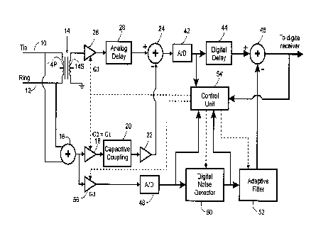
Figure 3 illustrates a noise cancellation circuit according to a second
embodiment
of the invention which compensates for loop imbalance. The noise cancellation
circuit
comprises a differential signal path comprising a hybrid transformer 14 having
its
primary winding 14P connected to the TIP 10 and RING 12 of a twisted-wire pair
subscriber loop. One end of its secondary winding 14S is grounded and the
other end
is connected to an input of a variable gain amplifier 26. The output of
amplifier 26 is
connected by way of an analog-to-digital converter 42 and digital delay unit
44 to a first
input of a digital adder 46. The adder 46 subtracts from the delayed
differential signal
CA 02273658 1999-06-07
8
a common mode noise estimate signal which is derived via a common mode signal
path
comprising the summer 16, a variable gain amplifier 18, a second analog-to-
digital
converter 48, a digital noise detector (DND) 50 and an adaptive filter 52. The
digitized
common mode signal is applied to the digital noise detector which detects the
frequency
bands in which there is significant noise and passes to the adaptive filter 52
only the
signal in those bands. The adaptive filter 52 is controlled by a control unit
54,
specifically a microcontroller, which has inputs connected to the differential
path at the
output of the A/D converter 42, to the common mode signal path at the output
of the
A/D converter 48, to the output of the digital noise detector 50 and to the
output of the
adder 46, which constitutes the output of the noise cancellation circuit. As
illustrated
by functional blocks 5.1 and 5.2 of Figure 5, which illustrates pertinent
functions of the
control unit/microcontroller 54, the latter also controls the gains of
amplifiers 26 and 18
to ensure that the signals applied to the A/D converters 42 and 48,
respectively, are
within their proper operating ranges.
The digital delay 44 is adjusted during manufacture to compensate for delay
introduced by summing device 16, amplifier 18, A/D converter 48 and digital
noise
detector 50. Although the adaptive filter 52 is in the common mode signal
path, it need
not be taken into account because its normal operation entails compensating
for delays.
It should be noted that the noise canceller of Figure 3 does not need quiet
periods
but will adapt the coefficients of adaptive filter 52 during normal operation.
Thus, in
operation, the common mode signal is digitized and applied to the digital
noise detector
50 which will detect significant noise signals; these noise signals are, of
course, most
likely to have been inductively coupled into the twisted-wire pair. Only the
portion of
the common mode signal in the noisy frequency bands will be passed to the
adaptive
filter 52 as the noise estimate signal. The control unit 54 monitors the cross-
correlation
between the output of the digital noise detector 50 and the output of the
output adder 46
and tunes the coefficients of the adaptive filter 52 so as to reduce the
correlation -
substantially to zero. A significant advantage of this embodiment is that it
does not
require a quiet period to tune the adaptive filter.
A preferred adaptive filter 52 processes the common-mode noise signal from
DND 50 such that it is as close as possible to the common mode noise component
of the
differential signal at the input to adder 46 by iteratively adjusting the
coefficients (tap
weights). The design of such an adaptive filter is known to persons skilled in
this art
CA 02273658 1999-06-07
9
and so is not further discussed here; a good description can be found in an
article by
Bernard Widrow et al. entitled "Adaptive Noise Cancellation: Principles and
Applications", Proceedings of the IEEE, Vol. 63, No. 12, December 1975, pp.
1692-
1716.
A suitable digital noise detector (DND) 50 is disclosed in copending Canadian
patent application No. 2,239,675 and will now be described with reference to
Figure 4.
In the digital noise detector 50, the digital common mode signal from A/D
converter 48
(Figure 3) is supplied to an analysis filter bank 60 which comprises a lowpass
filter 61,,
a plurality of bandpass filters 612 to 61r,1_, each having a different centre
frequency, and
a highpass filter 61M. The narrowband signals from the filters 611 to 61M are
supplied
to respective ones of a corresponding plurality of downsamplers 621 to 62M,
each of
which downsamples by a factor M. In this preferred embodiment, the
downsampling
rate M is equal to the number of subbands, i.e., the analysis filter bank 60
is uniformly,
maximally decimated.
The plurality of subband signals S, to 5,,,, are applied to a corresponding
plurality
of noise detection circuits 63, to 63,1, respectively, the outputs of which
comprise
respective subband noise estimate signals El to EM. The subband noise estimate
signals
E, to EM are supplied to respective inputs of a synthesis filter bank 64. The
analysis
filter bank 60 and the synthesis filter bank 64 are complementary and designed
to
provide "pseudo perfect reconstruction" as described earlier. Thus, synthesis
filter bank
64 comprises a plurality of upsamplers 651 to 65r,1 which receive and upsample
the digital
subband noise estimate signals El to E",1, respectively, by the factor M (the
same as the
downsampling rate in the analysis filter 60). The outputs of the upsamplers
651 to 65M
are supplied to a corresponding plurality of bandpass filters 661 to 66M,
respectively.
The outputs of the filters 661 to 66M are summed by summing device 67 for
output to the
adaptive filter 52 (Figure 3). It should be noted that the filters 66, to 66M
in the
synthesis filter bank 64 are not identical to the corresponding filters 61, to
61M in the
analysis filter bank 60. The relationship between the analysis filter bank 60
and the
synthesis filter bank 64, and especially the coefficients of their filters, is
known to those
skilled in this art and so will not be described in detail here. For details,
the reader is
directed to chapter 7 entitled "Multirate Signal Processing" of the text book
"Advanced
Digital Signal Processing: Theory and Applications", by G. Zelniker and F.
Taylor,
CA 02273658 1999-06-07
publ. Marcel Dekker, Inc. , and to the technical literature, including the
articles by
Akansu et al and by Crosier et al (supra).
The noise detection circuits 63, to 63M have identical structures so only one
circuit 63M, is shown in detail in Figure 4, for simplicity.
5 The components of the noise detection circuit 63M are controlled by a common
clock which, for convenience of illustration, is not shown. Within the noise
detection
circuit 63M, each sample value of the subband signal SM is applied to one
input of a
selector 68M, which may be a multiplexer, and to an absolute value device 69M
which
strips off the sign and supplies the sample value to an input of a delay bank
70M. The
10 outputs of the delay bank 70M are supplied in parallel to a summing device
71M, which
sums them and supplies the sum to a comparator 72M. The selector 68M is
controlled by
the output of the comparator 72M to select either the instant sample of the
subband signal
or a zero value and supply it to the corresponding input of the synthesis
filter bank 64.
The subband signal SM is clocked through the delay bank 70M continuously. The
values
in the delay bank 70M in any clock cycle are summed by the summing device 71M
and
the summation value compared with a threshold value TM. If the summation value
is
greater than the threshold value TM, the output of comparator 72M is a "1"
causing
selector 68M to select the instant sample value of the subband signal SM, and
supply it
as the digital noise estimate signal EM for channel M to the corresponding
input of
synthesis filter bank 64. If the summation value is less than the threshold T,
the
comparator 72M supplies a zero to selector 68M causing it to provide a zero
value as the
digital noise estimate signal EM. Thus, when the subband signal SM contains a
certain
common mode noise component, the instant sample value of subband signal SM is
supplied as the digital noise estimate signal EM. Otherwise, no value is
supplied.
The other noise detection and phase inversion circuits 63, to 63M_, produce
corresponding digital noise estimate signals E, to E,,,,_1 in a similar
manner.
The phase inversion units 63, to 63M use threshold values T, to TM,
respectively,
which are adjusted individually by the control unit 54 (Figure 3).
Generally, each threshold value will be selected according to the nature of
the
noise in the corresponding subband frequency band. In general, impulse noise
will tend
to be rather large in amplitude compared to radio frequency interference but
of shorter
duration. Consequently, each threshold value T, to TM may be selected so that
the
threshold value will be exceeded if a small number of segments of the
corresponding one
CA 02273658 1999-06-07
11
of the delay banks 70, to 70M contain relatively high values; or all of the
segments of the
delay bank contain somewhat lower values, as would occur with a radio
frequency
interference signal. Hence, the length of the delay banks 70, to 70M, any
scaling factors
of the signal supplied to the analysis filter bank, and the threshold would be
arranged or
could be adjusted to suit particular conditions prevailing in the vicinity of
the installation.
It should be appreciated that, although the specific embodiment uses a
uniformly,
maximally decimated analysis filter bank, other structures are feasible. For
example, the
analysis filter bank could provide a plurality of subband signals concentrated
at the
higher frequencies where radio frequency or impulse noise might be a greater
problem
due to the relatively lower energy of the transmitted signal.
For further information about the digital noise detector, and examples of the
various possible configurations for the digital noise detector 50, the reader
is directed to
the afore-mentioned Canadian patent application No. 2,239,675.
It should be noted that the digital noise detector 50 provides a history of
the
common mode signal over several samples. It has been proposed, however, in the
context of high speed digital subscriber loops, to detect noise in the
received signal by
comparing the power spectral density of each block of the received signal with
a
predefined desired spectral mask for the received (information) signal. If
that is done,
the digital noise detector 50 illustrated in Figure 4 could be modified by
omitting, in the
noise detectors 63, to 63r.,, the absolute value devices 69, to 69M, the delay
banks 70, to
70M, the summing devices 71, to 71M and the comparators 72, to 72M. The
subband
signals S, to SM then are applied directly to the selectors 68, to 68M,
respectively. The
microcontroller 54 will then supply control signals T, to TM directly to the
selectors 68,
to 68r,,, respectively. It should be appreciated that the signals T, to T~,,
will not be
threshold signals but rather 1 bit control signals to toggle the selectors.
It is also envisaged that the downsamplers 62, to 62M in the analysis filter
bank
60 and the upsamplers 65, to 65,,,, in the synthesis filter bank 64 might be
omitted. As
mentioned earlier, the passbands of the filters 61, to 61M and filters 66, to
66M must have
the required degree of overlap.
When such a modified digital noise detector is used, the control unit 54 will
compare the spectral power density of the received signal with a prescribed
power
spectral density mask or template to detect those bands in which significant
noise occurs.
Referring now to Figure 5, in step 5.3 the microcontroller 54 partitions the
received
CA 02273658 1999-06-07
12
differential signal from A/D converter 42 into blocks each of length N
samples, for
example 240 samples. In step 5.4, the microcontroller uses Fast Fourier
Transform
(FFT) to obtain the power spectral density of each block and, in step 5.5,
compares the
resulting spectral envelope with a spectral mask previously stored in the
microcontroller's memory (not shown). It is expected that the parameters of
the spectral
mask will be set by national or international standards on the basis of
experiments
conducted with various kinds of communications channels or loops.
In step 5.6, the microcontroller lists the frequency bands in which the power
spectral density of the block exceeds the envelope of the spectral mask and
stores the
information. In step 5.7, determines for each band whether or not the power
spectral
density exceeded the envelope in a predetermined number X of a predetermined
previous
number Y of the blocks. If it did, the microcontroller adj usts the
corresponding one of
the signals Tl to TM to select that band so that the digital noise detector 50
will sum the
common mode noise signal in each of those bands to produce the common mode
noise
signal for application to the adaptive filter 52.
It is important that the digital noise detector not introduce any extra noise
that
might be correlated in some way with the information signal. Similarly, the
DND
cannot afford to make frequent changes to its output, as such activity could
prevent the
adaptive filter from converging properly. This can be assured by providing a
suitable
length of delay banks 70, to 70M, where the DND of Figure 4 is used, and/or by
ensuring that the number of blocks X in step 5.7 is sufficient.
Figure 5 also illustrates the cross-correlation function of the
microcontroller 54,
which will be performed whether the digital noise detector 50 is as shown in
Figure 4
or modified as described hereinbefore. Thus, step 5.8 determines cross-
correlation
between the common mode signal from digital noise detector 50 and the system
output
from adder 46 and step 5.9 adjusts the coefficients of the adaptive filter 52
to reduce any
such correlation, ideally to zero.
Figure 6 illustrates a third embodiment of the invention which employs both
the
stray capacitive coupling compensation of the embodiment of Figure 1 and the
adaptive
filter compensation approach of the embodiment of Figure 3. As in both of the
first and
second embodiments, the TIP conductor 10 and RING conductor 12 are connected
to the
primary winding 14P of the hybrid transformer 14, the secondary winding 14S
having
one end grounded and the other end connected to the differential signal path,
i.e. to
CA 02273658 1999-06-07
13
variable gain amplifier 26. It should be noted, however, that the differential
path of the
circuit illustrated in Figure 6 comprises an analog portion formed by analog
delay device
28 and analog summer 24 and a digital portion formed by an A/D converter 42, a
digital
delay 44 and a digital adder 46, the output of the latter being the output of
the noise
cancellation circuit and applied to the usual receiver.
The circuit has both an analog common mode path similar to that shown in
Figure
1 and a digital common mode path similar to that shown in Figure 3. The summer
16
is shared by both paths. As in the embodiment of Figure 1, the analog common
mode
path comprises a variable gain amplifier 18, which has a gain G2 proportional
to the gain
G1 of variable amplifier 26, a capacitive coupling device 20 and an inverting
amplifier
22, the output of which is connected to the second input of summer 24, as
before. In
this circuit, however, the output of analog summer 24 is digitized by A/D
converter 42
and supplied to digital delay 44 which supplies the delayed differential
signal to a first
input of digital adder 46. The output of summer 16 is also supplied to an
input of a
third variable gain amplifier 56 which has a gain G3. The output of the
amplifier 56 is
digitized by second A/D converter 48 and supplied to the digital noise
detector 50 and
the control unit 54' which detects the noisy bands and passes only the signals
in those
bands to the adaptive filter 52. As in the embodiment of Figure 3, the control
unit/microcontroller 54 receives inputs also from the respective outputs of
A/D converter
42, digital adder 46, and digital noise detector 50.
The control unit 54' will differ from the control unit 54 of Figure 3 because
it
will control the gains G1, G2 and G3 of the three amplifiers 26, 18 and 56,
respectively.
Its control of the adaptive filter 52 will be as described with reference to
Figures 3 and
4 or Figures 3 and 5, i.e. using threshold control signals or selector control
signals,
depending upon the nature of digital noise detector 50. As before, if the DND
50 shown
in Figure 6 is that shown in Figure 4, which performs historical analysis of
the received
signal, the microcontroller 54 need not conduct spectral analysis. If the DND
50 does
not perform historical analysis, the microcontroller 54 will perform the
spectral analysis
and comparison described with respect to Figure 5.
The invention embraces various other modification and improvements to the
above-described embodiments. Thus, control unit 54 could extract differential
and
common mode signals from other points in the differential signal path and
common mode
signal path, respectively.
CA 02273658 1999-06-07
14
It should be appreciated that the various aspects of the invention are not
necessarily limited to noise cancellation in twisted pair subscriber loops but
could be
applied to other communications channels, in which case the input means might
not be
a hybrid transformer. For example, the embodiment of Figure 3 could be used
with
communications channels which employ coaxial cables, comprising a coaxial
shield and
one or more inner conductors. In such a case, the hybrid transformer shown in
Figure
3 would be omitted and the coaxial shield connected directly to the input of
amplifier 18.
Where a single inner conductor was used, it would be connected directly to the
input of
amplifier 26. If two or more inner conductors were used, they would be
interfaced to
the noise detection circuit by way of a suitable matching transformer.
It should be appreciated that, although the above-described embodiment of the
invention use analog components to provide the compensation for the capacitive
coupling, the compensation could be implemented digitally, perhaps using a
digital signal
processor.
INDUSTRIAL APPLICABILITY
Embodiments of the invention advantageously provide noise cancellation for
communications channels, such as telephone subscriber loops, which compensates
for the
effects of stray capacitive coupling in the hybrid and/or impedance imbalance
effects in
the communications channel yet do not require a quiet period for training
purposes.