Note : Les descriptions sont présentées dans la langue officielle dans laquelle elles ont été soumises.
CA 02273778 1999-06-09 ,
PC758 - 1 -
TELECOMMUNICATIONS SYSTEM OF THE WAVELENGTH DIVISION
MULTIPLEXING TYPE COMPRISING AN OPTICAL CHANNEL ANALYSER
s
The present invention relates to a system and a method of optical
telecommunication, particularly suitable for wavelength division multiplexing
transmission, or WDM, in which the various signals are monitored throughout
the
telecommunication path, in the transmitter, in the intermediate stations for
1o amplifying the said signal, and in the receiver.
For wavelength division multiplexing, or WDM, transmission, it is
necessary to send a plurality of transmission signals which are independent of
each
other along the same line, which consists of optical fibres, by multiplexing
in the
domain of the optical wavelengths; the transmitted signals may be either
digital or
15 analog, and they are distinguished from each other in that each of them has
a
specific wavelength, separate from those of the other signals.
The implementation of this WDM transmission requires that specific
wavelengths of predetermined amplitude, termed "channels" in the following
text,
be assigned to each of the signals at different wavelengths. These channels,
2o identified in the following text by a wavelength value, known as the
central
wavelength of the channel, have a certain spectral amplitude about t<he
central
wavelength value, which depends, in particular, on the characteristics of the
laser
which is the source of the signal and on the modulation imparted to it to
associate a
data element with the signal. Typical values of spectral amplitude of the
signal
25 emitted by a laser, in the absence of modulation, are around 10 MHz; in the
presence of an external modulation, at 2.5 Gbit/s for example, the spectral
amplitude is approximately 5 GHz.
In order to transmit signals in a large number of channels, making use of
what is known as the third transmission window of the silica fibres and of the
3o bandwidth of the optical amplifiers (for example from 1525 to 1565 nm or
from
1540 to 1620, or again from 1525 to 1620), the wavelength separation between
the
CA 02273778 1999-06-09
PC758 - 2 -
channels is conveniently of the order of a number of nanometres or fractions
of
nanometres.
For the correct reception of these transmission signals, it is necessary to
make a separation between the signals, to guide them to the corresponding
users.
Moreover, during their travel along the line the signals may undergo
alterations
due to external agents; these alterations may affect the power of the signal
according to the wavelength. This is because signals whose wavelengths differ
from each other may undergo alterations which differ from each other, with the
result of obtaining, after demultiplexing, channels having a better
transmission
to quality than others. It therefore becomes necessary to extract these
signals in order
to monitor and if necessary carry out an energy rebalancing on them at various
points of the telecommunication line.
To extract these signals, use is made of optical filters with narrow bands,
through which only the signal in the selected channel can pass, in order to
ensure
the absence of unwanted signals, which would constitute noise if superimposed
on
the selected signal. However, the use of these filters requires both a high
stability
of the wavelength of the transmitted signal and a high intrinsic stability of
the
central wavelength of the filters.
Additionally, if the number of channels is high, the pass band of the filters
2o must be sufficiently narrow. Filters having a narrow pass band and high
insulation
between one channel and the next are expensive and difficult to obtain on the
market, owing to problems of reproducibility on an industrial scale.
Patent application EP 0 629 885 proposes the use of two Bragg reflection
filters connected in series in each channel selection filter. The pass band is
obtained by suitable positioning of the two reflection peaks of the filters.
US patent 5.504.609 describes a demultiplexer for selecting a particular
channel from the multiplexed signal and supplying it to the receiver. To catty
out
the channel selection, the multiplexed signal is sent to an optical filter
through a
coupler. The wavelength of the channel is reflected by the optical filter to
the
3o receiver through the coupler. The optical filter comprises a Bragg grating
element
which reflects the wavelength of the channel and transmits all the others.
E
' CA 02273778 1999-06-09
PC758 _ 3 _
Patent application EP 0 713 110 describes the use of a filter consisting of a
fibre which incorporates a normally reflecting Bragg grating filter and two
inclined
Bragg grating filters. This fibre is connected to one port of an optical
circulator.
US patent 5,039,201 describes a Fabry-Perot filter which comprises a pair
of reflecting surfaces and a pair of optical elements whose refractive indices
are
different from each other, disposed in such a way as to form two resonant
cavities
tuned to the same frequency. The reflecting surfaces are disposed in such a
way as
to send a beam of light emerging from the first cavity to the second cavity,
and
vice versa. This produces a double filtering at the same frequency; this
frequency
to can be regulated by modifying the characteristics of both cavities.
US patent 6,633,743 describes a device which comprises a Fabry-Perot
filter used between two amplification stages. In one embodiment of the device,
the
optical signal passes for a first time through the filter, the output signal
is back
reflected by suitable reflection means and reinjected into the filter, using
the same
t5 optical path. An optical circulator disposed at the input of the filter
separates the
signal entering the filter from that emerging after the back reflection. In
this device,
therefore, the optical signal is doubly filtered.
The applicant has observed that in these structures the phenomenon of back
reflection of the optical signal by a filter, in other words the reflection of
the part of
2o the signal which is not transmitted beyond the filter, may give rise to
problems of
instability in the structure by adding a considerable quantity of noise to the
filtered
signal. This is because a phenomenon of successive reflections of the said
part of
the signal which causes noise (crosstalk) may develop between the filter and
the
means of back reflection.
25 The applicant has tackled the problem of making the identification of these
signals less critical in a transmission system of the wavelength division
multiplexing type, at various points of this system, by means of precise
filtering.
It has been found, in particular, that by making the WDM signal pass at
least twice through a tunable filter tuned to each channel in sequence, each
signal is
3o extracted with high resolution and low noise. In this double pass,
switching and
delay means are provided which are capable of limiting the negative
consequences
of the previously described phenomenon of back reflection of the filter.
', CA 02273778 1999-06-09
PC758 - 4 -
Advantageously, if the double pass of the signal through the filter always
takes
place in the same direction, the effects of the preceding phenomenon are
negligible.
In a first aspect, the present invention relates to an optical
telecommunications system, comprising:
- at least one transmission station, comprising a generator of transmission
signals at a minimum of two predetermined wavelengths, and a wavelength
division multiplexer for sending the said transmission signals along an
optical fibre
line;
- at least one station for receiving the said transmission signals;
- the said optical fibre lire connecting the said transmission and receiving
stations:
- a station for amplifying the optical signal, disposed along the said line;
- a control unit associated with the said line station,
characterized in that it has an optical channel analyser disposed down-stream
from
the said amplifying station and connected to the said control unit.
In particular, the said channel analyser comprises:
- a device for extracting part of the optical signal from the line at an input
optical fibre;
- at least one selective filter tunable to the wavelengths of the channels
which
contain the signals;
- a circuit capable of causing at least a double pass of the optical signal
through the said filter;
- a device for detecting the filtered optical signal;
- a circuit for reading the electrical signal originating from the said
detecting
device.
Preferably, the said circuit capable of causing at least a double pass of the
optical signal through the said filter comprises:
- a first switch, operated by a driver circuit, which comprises a first port,
3o connected selectively to one of two second ports;
- a second switch, operated by a driver circuit, which comprises a first port,
connected selectively to one of two second ports;
. '. CA 02273778 1999-06-09
PC758 - S -
- - an isolator disposed between the said first port of the first switch and
the
said filter;
- at least one delay fibre disposed at the output of the said filter;
- one of the said second ports of the first switch being connected to the said
input fibre and the other being connected to one of the two second ports of
the
second switch;
- the said first port of the second switch being connected to the said optical
delay fibre;
- the said second port of the second switch being connected to the said
detecting device.
Alternatively, the said circuit capable of causing at least a double pass of
the optical signal through the said filter comprises:
- a switch, operated by a driver circuit, which comprises a first port,
connected to the input of the said filter, connected selectively to one of two
second
ports, one of which is connected to the said input fibre while the other is
connected
to the said detecting device;
- at least one delay fibre disposed at the output of the said filter;
- a device for reflecting the optical beam emerging from the said delay fibre.
In particular, the said detecting device is a photodiode.
2o In particular, the said circuit for reading the electrical signal
originating
from the detecting device comprises a first amplification and current-voltage
conversion stage, connected in series with a second voltage amplification
stage,
connected in series with a first port of a switch which is connected
selectively to
one of two second ports, each of which is connected to one input of a circuit
that
integrates the difference between the said two inputs.
According to a further aspect, the present invention relates to a channel
analyser for wavelength division multiplexed transmission signals, comprising:
- an input for the said v~~avelength division multiplexed transmission signal;
- at least one selective filter tunable to the wavelength of the channels
which
contain the signals;
- an optical circuit capable of causing at least one double pass of the
optical
signal through the said filter;
', CA 02273778 1999-06-09
PC758 - 6 -
~ - a device for detecting the filtered optical signal,
characterized in that the said optical circuit comprises at least one optical
switch
and a delay fibre associated with the said at least one switch.
Preferably, the said circuit capable of causing at least a double pass of the
optical signal through the said filter comprises:
- a first switch, operated by a driver circuit, which comprises a first port,
connected selectively to one of two second ports;
- a second switch, operated by a driver circuit, which comprises a first port,
connected selectively to one of two second ports;
io - an isolator disposed between the said first port of the first switch and
the
said filter;
- at least one delay fibre disposed at the output of the said filter;
- one of the said second ports of the first switch being connected to the said
input fibre and the other being connected to one of the two second ports of
the
second switch;
- the said first port of the second switch being connected to the said optical
delay fibre;
- the said second port of the second switch being connected to the said
detecting device.
2o Alternatively, the said circuit capable of causing at least a double pass
of
the optical signal thmugh the said filter comprises:
- a switch, operated by a driver circuit, which comprises a first port,
connected to the input of the said filter, connected selectively to one of two
second
ports, one of which is connected to the said input fibre while the other is
connected
to the said detecting device;
- at least one delay fibre disposed at the output of the said filter;
- a device for reflecting the optical beam emerging from the said delay fibre.
In particular, the said detecting device is a photodiode.
Preferably, the said circuit for reading the electrical signal originating
from
the detecting device comprises a first amplification and current-voltage
conversion
stage, connected in series with a second voltage amplification stage,
connected in
series with a first port of a switch which is connected selectively to one of
two
'. CA 02273778 1999-06-09
PC758 - 7 -
- second ports, each of which is connected to one input of a circuit that
integrates the
difference between the said two inputs.
According to a further aspect, the present invention relates to a method for
filtering an optical signal in a waveband, characterized in that it comprises
the
following stages:
- extracting a time sample of the said signal;
- filtering the said time sample of the signal for a first 'time by means of a
filter;
- filtering the signal for a second time by means of the same filter;
- converting the said doubly filtered optical signal into a corresponding
electrical signal.
According to a further aspect, the present invention relates to a method for
monitoring channels for wavelength division multiplexed transmission signals,
characterized in that it comprises the following stages:
- extracting from a line containing multiple-wavelength signals a time
sample of the said signal;
- filtering the said time sample of the signal for a first time by means of a
tunable filter;
- filtering the signal for a second time by means of the same filter;
- converting the said doubly filtered optical signal into a corresponding
electrical signal;
- sending this electrical signal to a terminal for monitoring the parameters
of
the line.
In particular, the said method additionally comprises the stage of tuning the
said filter to a different spectral region.
According to a further aspect, the present invention relates to an optical
amplifier with gain control, comprising:
- at least one active fibre doped with a rare earth and capable of generating
a
light emission of a multiple-wavelength transmission signal in response to
light
3o supplied at a pumping wavelength;
- at least one pumping source of the said active fibre at the said pumping
wavelength;
CA 02273778 1999-06-09
PC758 - 8 -
- - a coupling device for sending the said light supply and the said
transmission signal along the active fibre,
characterized in that it comprises an optical channel analyser, disposed at
the
output of the said active fibre, communicating the information on the detected
optical channels to a control unit which regulates the gain of the amplifier.
Preferably, the said control unit controls and regulates the power of the said
pumping source.
Alternatively, the said control unit controls a variable attenuator disposed
at
the output of an amplification stage.
to Further details may be obtained from the following description, with
reference to the attached drawings in which are shown:
in Figure 1, a diagram of a telecommunications system of the wavelength
division
multiplexing type according to the present invention;
in Figure 2, a channel analyser according to one embodiment of the present
invention;
in Figure 3, a channel analyser according to a further embodiment of the
present
invention;
in Figure 4, the graph of the operating signals of the switches of the device
shown
in Figure 3;
2o in Figure 5, a driver suitable for use in the present invention for
generating the
signals shown in Figure 4;
in Figure 6, a possible reading circuit for the channel analyser according to
the
present invention;
in Figure 7, an apparatus for the experimental tests which comprises the
channel
analyser according to the present invention;
in Figure 8, the response of the structure shown in Figure 3, in the cases of
single
and double pass with a white spectrum, in other words with a constant
intensity in
wavelength;
in Figures 9a-9e, the spectra in decibels measured for five pairs of signals
3o separated by different wavelength intervals in the WDM signal in the case
of a
single pass and in the case of filtering with the device according to the
present
invention.
CA 02273778 1999-06-09
PC758 - 9 -
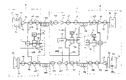
- Figure 1 shows schematically a bidirectional optical telecommunications
system of the wavelength division multiplexing type, comprising two terminal
stations T and R, each of which includes a corresponding transmission station
1 A,
1 B and a corresponding receiving station 2A, 2B.
In particular, in the version shown in Figure 1, the transmission station lA
comprises 16 transmitters of optical signals having a first set of
wavelengths,
indicated by odd-numbered indices, ~,,, ..., ~,3, (for example, those included
in the
1530-1565 nm waveband), and the transmission station 1B comprises 16
transmitters of optical signals having a second set of wavelengths, indicated
by
io even-numbered indices, 7~,z, ..., ~,3Z.
The number of independent wavelengths used for the signals of each
transmission station is not limited to the value of 16 indicated in the
described
device, and may have a different value: The number of wavelengths,
corresponding
to the number optical channels which can be used for transmission in each
direction, may be selected according to the characteristics of the
telecommunications system.
The optical transmitters included in the transmission stations 1 A, 1 B are
transmitters with direct modulation or external modulation, according to the
requirements of the system; in particular, these requirements are related to
the
chromatic dispersion of the optical fibres of the system, to their wavelength
and to
the specified transmission speed.
The outputs of each of the transmitters of the transmission stations lA, 1B
are connected to the multiplexers 3A, 3B respectively, each of which combines
the
corresponding optical signals towards a single output, in other words to the
optical
fibres 101 and 102 respectively, which are connected to the inputs of optical
power
amplifiers SA, 5B respectively.
In general, the multiplexers 3A and 3B are passive optical devices, by means
of
which the optical signals transmitted along corresponding optical fibres are
superimposed in a single fibre; devices of this kind consist, for example, of
3o couplers of the fused fibre, planar optics, micro-optics or similar types.
CA 02273778 1999-06-09
PC758 - 10 -
By way of example, a suitable multiplexer is that marketed under the
symbol SMTC2DOOPH210 by E-TEK DYNAMICS INC., 1885 Lundy Ave., San
Jose, CA (USA).
The power amplifiers SA, SB raise the level of the signals generated by the
transmission stations lA, 1B to a sufficient value for them to travel along
the next
section of optical fibre present before the receiving station or amplifying
means
which maintain a sufficient power level at the end to provide the required
transmission quality.
For the purposes of the present invention, and for the application described
1o above, optical fibre amplifiers of the commercial type, having an input
power of
-13.5 to -3.5 dBm and an output power of at least 13 dBm, for example, are
suitable for use as the power amplifiers SA and SB.
An example of a suitable model is the TPA/E-MW, marketed by the
applicant, and making use of an erbium-doped active optical fibre.
The power amplifiers SA and SB are then connected to an optical line
section 103 and an optical line section 104 respectively, normally consisting
of a
single-mode optical fibre, of the step index type, inserted in a suitable
optical cable
with a length of a few tens (or hundreds) of kilometres; for example,
approximately
100 kilometres with the amplification means described below and the indicated
power levels.
At the end of each of the said optical line sections 103 and 104 there are
one or more stations A for amplifying the optical signal, each of these
stations
comprising line amplifiers 6A and 6B, capable of receiving the signals which
are
attenuated during their travel along the fibre, and of amplifying them to a
sufficient
level to supply them to a plurality of subsequent optical line sections 105
and 106
respectively, thus covering the total transmission distance required to reach
a
preamplifier 7A and a preamplifier 7B respectively or a further amplification
station A. In the context of the present invention, the term "preamplifier"
signifies
an amplifier designed to compensate for the losses of the last optical line
section
3o and the insertion losses of the subsequent demultiplexing stages 8A or 8B,
in such
a way that the signal at the input of the receiving stations has a suitable
power level
for the sensitivity of the device. The preamplifier also has the function of
limiting
CA 02273778 1999-06-09
PC758 - 11 -
the dynamics of the signals, by reducing the variation of the power level of
the
signals at the input of the receiver with respect to the variation of the
power level
of the signals received from the transmission line. One type of preamplifier
suitable for use as a preamplifier 7A or 7B is, for example, an optical
amplifier of
s the commercially available erbium-doped active optical fibre type, having a
total
input power of -20 to -9 dBm and an output power of 0-6 dBm.
A suitable model is, for example, the 1ZPA/E-MW, marketed by the
applicant.
The multiplexed optical signals in two input ports connected to the outputs
of the preamplifiers 7A and 7B arrive at the demultiplexers 8A, 8B
respectively,
which are capable of separating into 16 output optical fibres, according to
the
corresponding wavelengths, 16 signals which will be sent to the corresponding
16
receivers included in the receiving stations 2A and 2B: A delnultiplexer
suitable
for use in the present transmission system is, for example, the demultiplexer
described in patent application No. ITAMI970054 in the name of the present
applicant.
If the optical signals to be transmitted are generated by sources of signals
which have intrinsic transmission characteristics (such as wavelength, type of
modulation, power) different from those specified for the connection
described,
2o each transmission station 1 A, 1 B comprises interfacing units, 901, .. .,
931 and
902, ..., 932 respectively, capable of receiving the optical signals generated
by the
transmission stations lA, iB, of detecting them, of regenerating them with new
characteristics suitable for the transmission system, and of sending them to
the
multiplexers 3A, 3B.
In particular, the said interfacing units generate the corresponding working
optical signals mentioned previously, having wavelengths ~,,, ..., 7v,3, and
~, ..., ~2
respectively which are suitable for the requirements of the system, as
described
below.
US Patent 5.267.073 held by the present Applicant describes interfacing
3o units comprising, in particular, a transmission adapter capable of
converting an
input optical signal into a form suitable for the optical transmission line,
and a
CA 02273778 1999-06-09
' PC758 - 12 -
receiving adapter, capable of reconverting the transmitted signal into a form
suitable for a receiving unit.
For use in the system, the transmission adapter preferably comprises an
externally modulated laser as the source for the generation of the output
signal.
As an alternative to the use of interfacing units 901, ..., 931 and 902, ...,
932, one or more of the laser transmitters included in the transmission
stations lA,
1B may be laser transmitters operating at the predetermined wavelengths, for
example transmitters using DFB lasers at the wavelengths ~,,, 7~.;, ..., 7~,3,
and ~,
~,,,..., 7.32 respectively. Preferably, the wavelength of each of the sources
used for
1o the signals is stable within +/- 0.25 nm, more preferably within +/- 0.1
nm.
The present optical fibre telecommunications system provides, in addition
to the channels intended for the communication signals and made available to
the
users, an independent channel capable of transmitting service signals. A
system
comprising channels intended for service signals is described in US Patent
5113459 in the name of the applicant.
These service signals may be of various types, for example signals for the
alarm system, for monitoring or controlling equipment disposed along the line,
such as repeaters or amplifiers, or communications between the maintenance
personnel operating at one point of the line and an intermediate or terminal
station
of the line.
The amplifiers SA, 6A, 7A and SB, 6B, 7B, and any further line amplifiers
not shown in Figure 1, are generally designed to receive and/or transmit
control
signals, for example those for the activation or verification of the operation
of
some of their components, and are also subject to maintenance operations for
which an operator may need to communicate with the terminal stations T or R,
for
transmission and reception, or with the other intermediate amplification
stations A.
In these cases, therefore, it is necessary to introduce into the
communication line fiuther signals, which can be received and transmitted at
any
intermediate station or at the terminal stations. These service signals are
3o transmitted at a wavelength significantly different from the communication
wavelength, in other words one that can be separated by means of a suitable
dichroic coupler.
CA 02273778 1999-06-09
PC758 - 13 -
Additionally, these amplifiers, whose internal configuration is not
illustrated, generally comprise at least one active fibre doped with a rare
earth,
capable of generating an amplification of the multiple-wavelength transmission
signal in response to a supply of light radiation at a pumping wavelength.
This pumping wavelength is different from that of the transmission signals
and is produced by at least one pumping source of the said active fibre,
having an
optical power controllable by a control unit 18 of the station A, T or R
within
which the amplifier is located; by way of example, this source may be a laser.
The
amplifier also comprises a coupling device for sending the said pumping
radiation
to and the said transmission signal along the active fibre.
The control unit 18, also called a CMP (Control and Monitoring Processor),
comprises a unit for the control and monitoring of the station parameters,
such as
the previously mentioned power of the pumping source, and also alarms, state
signals, signals which cause actions, etc., monitors the state of the station
on the
basis of the parameters, and transfers these data to a unit of the LCI (Local
Craft
Interface) 19, which controls the monitoring of the individual station by an
operator responsible for the maintenance of the station, or communicates,
through a
connection unit 17 which is also called an LSM (Line Service Module), with the
other stations of the network by means of which the said service signals are
2o propagated along the line.
For this purpose, two dichroic couplers 107 are present, as shown in Figure
1, at the input and output of each optical line amplifier 6A and 6B. The
dichroic
couplers 107 are devices capable of receiving at a common input the
communication signals and the service signals, which have different
wavelengths
multiplexed in the same fibre, and of separating at the output, into two
output
fibres 107a and 107b respectively, the communication signals at one or more
wavelengths and the service signals at a different wavelength. Examples of
dichroic couplers suitable for use in the present invention are, for example,
fused
fibre couplers, interference couplers, and couplers using Bragg grating
filters, for
3o example in combination with an optical circulator or an optical power
divider.
CA 02273778 1999-06-09
PC758 - 14 -
These couplers are also used to carry out the opposite function, in other
words to send along a single output fibre the communication signals and the
service signals which have been separately injected into the fibres 107a and
107b.
Similar dichroic couplers are present at the terminal stations at the outputs
of the power amplifiers SA and SB and at the inputs of the preamplifiers 7A
and
7B. Each dichroic coupler 107 is connected, by the corresponding fibre 107b
carrying the service signals, to the corresponding connection unit 17. By
means of
these units, the optical service signals leaving the coupler 107 are received
and
converted into corresponding output electrical signals, and/or electrical
input
io signals are converted into optical signals at the service wavelength and
injected
into the input of the fibre 107b of each dichroic coupler 107 to be
multiplexed
along the line.
In this way, an optical signal, at 1480 nm or at another wavelength used to
transmit service signals, extracted from the optical line of the dichroic
coupler 107,
is converted into a corresponding electrical signal, which can be used for the
applications specified for it, such as telephonic service communications of
the
maintenance personnel or monitoring of the line amplifier, or for further
control or
monitoring operations; similarly, control signals or telephonic service
communications can be sent along the output fibre from the line amplifiers to
reach
other destinations.
To enable the service signal to reach amplifiers or terminal stations located
at a great distance from the place of transmission of the signal, along a
fibre having
a plurality of optical amplifiers, each connecting unit 17 may comprise a
corresponding electronic service amplifier, so that the service signal can be
suitably amplified before being sent along the next section of optical fibre,
to the
destination station or to a new optical amplifier.
In this way, the service signal is amplified autonomously, in each optical
line amplifier, and can therefore cover the whole of the required distance,
reaching
the destination at a level sufficient for the objects assigned to it.
3o Although the injection and extraction of the service signals into and from
the optical line is conveniently executed at the terminal stations of the line
and in
the line amplifiers, as described previously, dichroic couplers and
corresponding
CA 02273778 1999-06-09
PC758 - 15 -
- stations for receiving and transmitting service signals may also be
introduced at
any other point of the optical fibre line where they are required.
The present embodiment of a WDM optical fibre communication system
also provides for the connection of an optical channel analyser 50, also shown
as
OCA (Optical Channel Analyser), which is a unit capable of monitoring, along
the
optical line, at the intermediate amplification stations A or near each
terminal
station T or R, the various characteristic values of the optical signal, such
as the
power level of the signal, the signal to noise ratio, the wavelength of the
transmission channel and the number of channels which are propagated along the
line.
The optical channel analyser 50 is a modular component which is
preferably connected along the line in the optical signal amplification
stations A,
and if necessary in the transmitter and in the receiver, and is capable of
monitoring
the signals which appear at each of these stations.
This device is advantageously connected in the transmitter after the power
amplifiers SA and SB, and at the output of the preamplifiers 7A and 7B in the
receiver.
Additionally, this device is preferably connected in the amplification
stations at the outputs of the line amplifiers 6A and 6B in the case in which
the said
2o amplification station on the line has an optical signal extraction and
injection
device, which causes a change in the information travelling along the various
channels. An optical channel analyser 50, of the type described,
advantageously
enables this variation to be monitored.
Additionally, although the analysis of all the channels is conveniently
carried out at the points described above, these channels may be extracted at
any
other point along the optical fibre line where this may be necessary.
As illustrated in Figure 1, each OCA is connected optically at the specified
points between extraction devices 108. They are capable of extracting part of
the
communication signal and are disposed, for example, in series with the
dichroic
3o couplers 107 disposed at the outputs of the power amplifiers SA and SB, in
series
with the directional couplers 107 connected at the outputs of the line
amplifiers 6A
CA 02273778 1999-06-09
- PC758 - 16 -
and 6B and at the output of each line amplifier not shown in Figure 1. Further
extraction devices 108 are disposed at the outputs of the preamplifiers 7A and
7B.
An extraction device 108 suitable for the purpose described is a directional
coupler which comprises two output optical fibres between which the
communication signal received at the input is distributed. The power
percentage of
the extracted signal is, for example, in the range from 0.1% to 0.5%, and is
preferably approximately 0.5%.
Each optical channel analyser OCA described in the present embodiment of
the invention is provided with a connection 502 such as a digital bus
(according to
to the ethernetTM standard, for example) which transmits information relating
to the
communication channels to andr'or from the control unit i 8. Additionally,
each
OCA module is preferably capable of receiving information from signals which
travel along the line in both directions. The directional couplers are
therefore
disposed at each intermediate station on both sections of the bidirectional
line.
The data received by the analyser SO are made available in the same station
by the control unit 18. The said data, or some of them, are sent along the
network
by the connection unit 17 in such a way that they are made available to the
equipment for the control and analysis of the whole network.
A telecommunications line as described comprises a channel analyser
2o which makes it possible to measure the parameters cited previously for each
transmission channel with high accuracy. In particular, an example of an
application specified for the analyser is that of counting the number of
signals
present in the dif~'erent output channels of the station, and of intervening
in the
regulation of the gain of the amplifier of the station, for example by
communicating with the unit which controls the pumping source of the
amplifier,
according to the number of signals which this station is retransmitting to the
next
station or to the receiver. Alternatively, the power of the amplifiers may be
controlled by the control unit 18 of the station, which controls a variable
attenuator
disposed at the output of the station, in such a way as to adjust the power of
the
3o channels.
A further example of the application of the channel analyser in a transmitter
is that of monitoring the power level of all the channels which make up the
WDM
CA 02273778 1999-06-09
PC758 - 17 -
signal to be sent along the line, and then transmitting the data to the
control unit,
which rebalances the channels by establishing the same power level for all the
channels.
In general, therefore, within each amplification station of a
telecommunications line the control unit 18 receives the data on the state of
the
system from the analyser S0, establishes the new configuration of the station
and
determines the corrective actions which are required.
Additionally, in a transmitter the monitoring of the output signals from it
and the consequent transmission of these parameters to the control unit 18 may
to result in an independent action in each channel by the transmitter to give
rise to a
balancing between the channels according to the characteristics required by
the
network.
Advantageously, these data may be transmitted, at the specific request of
the controller of the whole network and through the aforementioned service
channel, to any of the other stations of the network.
Figure 2 shows a first embodiment of a channel analyser 50.
The channel analyser comprises an optical switch 51 with a first port SO1
connected selectively to one of two second ports, namely 1 or 0. The
selection, of
the electrical type for example, is managed by a driver circuit 52.
2o This device 50 also comprises an input optical fibre 53 connected to one of
the second ports 0 of the optical switch 51, and a tunable filter 54 whose
input port
is connected optically to the port 501 of the switch. The remaining second
port 1 of
the optical switch 51 is connected through an output fibre 55 to a detecting
device
56, for example a photodiode associated with a reading device 57. The output
port
of the filter 54 is connected through a delay fibre 58 to a mirror 59.
The operation of the device shown in Figure 3 is as follows.
An optical signal present at the input optical fibre 53 is sent, through the
switch 51, which has its port 0 connected to the port 501, to the filter 54 in
which it
undergoes a first filtering. The part of the signal back reflected from the
filter, in
other words what is known as the back reflection, containing the reflected
signal at
all the wavelengths including the wavelength which is to be analysed (of which
a
small proportion, which in any case is negligible, is present), is reinjected
into the
CA 02273778 1999-06-09
PC758 - 18 -
input fibre 53. Consequently, this back reflection, which does not carry the
significant signal contained in the channel which is to be analysed at this
instant,
does not reach the detecting device 56. The switch 51 is then switched, and
connects the port 501 to the port 1 after a period t following the preceding
switch.
A signal pulse having the duration t is then sampled at the port 501 of the
switch
51.
The said signal pulse reaches the filter 54; it passes through the delay line
58 over a period i; it is reflected back into the delay line 58 by the mirror
59; and it
is then filtered for a second time at the same wavelength by the filter 54.
The said
1o delay line 58 and the driver circuit 52 are designed in such a way that the
signal
pulse passing through them, determined by the switching time of the switch 51,
is
present at the port 501 when the switch 51 has connected this port to the port
1.
From this port, the doubly filtered signal pulse reaches the photodiode 56 and
then,
in electrical form, the reading circuit 57.
In a successive instant, after the signal pulse has passed completely through
the port 1, the switch 51 returns to the initial condition so that a second
pulse can
be analysed. The operation of the device is repeated in an identical way for
successive signal pulses.
The optical switch 51 is a switch which must principally have the
2o characteristic of maintaining a high degree of optical isolation at the
unconnected
port, to ensure that the data received from the reading device are reliable.
The
switching speed of the switch is also an important parameter, since the length
of
the delay fibre is determined according to this speed, as well as according to
the
length of the said signal pulse.
A mechano-optical switch ensures a high degree of isolation, but at present
the available switches provide a switching frequency of not more than 1 kHz,
the
corresponding length of the delay fibre being 120 km. This length of the delay
fibre is a critical parameter for this type of switch.
An electro-optical switch provides a lower degree of isolation than a
3o mechano-optical switch, but achieves markedly higher switching speeds of at
least
100 kHz, corresponding to a delay fibre. length of approximately 1 km.
CA 02273778 1999-06-09
PC758 _ 19 _
The photodiode is, for example, an InGaAs PIN photodiode such as the
ETX75 FJ SLR model, marketed by EPITAXX OPTOELECTRONICS DEVICES,
7 Graphics Drive, West Trenton, NJ, USA.
A suitable filter for use in the analyser 50 is a filter which causes the
transmission of the wavelength which is to be analysed. The invention makes it
possible to use filters with high back reflection in all or some of the other
wavelengths which make up the WDM signal. However, it is also possible to use
filters having a relatively low back reflection, where these are available.
A tunable filter suitable for the indicated application is, for example, a
io Fabry-Perot filter, such as the FFP-TF model, marketed by MICRON-OPTICS,
Inc., 2801 Buford Hwy, Suite 140, Atlanta., Georgia, US, or the MF 200 model
marketed by QUEENSGATE INSTRUMENTS Ltd., Silkwood Park, Ascot,
Berkshire SLS 7PW, UK.
Alternatively, this filter may comprise a set of filtering elements (such as
Bragg gratings in fibre or interference filters) and/or other optical
components
(such as optical circulators or couplers) which in combination provide the
desired
filtering function.
The applicant notes that in this embodiment there is a double pass through
the Fabry-Perot filter which increases its spectral selectivity. Additionally,
the
2o optical signal is modulated not as a result of the coefficient of
reflection of the
mirror 59 but by means of the said switch 51, which enables the photodiode 56
not
to receive reflected power except during the two switching instants in which
the
switch resembles a coupler with a rapidly variable coupling factor.
For Fabry-Perot filters there may be a variation with time of the wavelength
on which is centred the Airy function which represents its transmission
function.
Between two successive signal pulses, therefore, the filter may be centred on
slightly different wavelengths. However, if the frequency of the modulation
introduced by the switch is sufficiently high, this difference may be
considered
negligible for the purposes of the invention.
3o In particular, if S(~.) is taken to be the spectrum of the pulse at the
input of
the device shown in Figure 2, and, as stated previously, A(~,) is the
transmission
CA 02273778 1999-06-09
PC758 - 20 =
function of the Fabry-Perot filter and B(~,) is that for the back reflection
of the
filter, a single pulse at the input of a device as shown in Figure 2
generates:
- a first contribution to the photodiode, equal to AZ(~,)S(~,),
- in the next time interval, a second contribution to the photodiode, due to
the
pulse filtered for a first time and then reflected by the mirror 59 and
filtered again,
in other words equal to AZ(~,)B(~.)S(~,);
the contribution B(~,)S(~,) due to the back reflection does not reach the
photodiode,
since it is generated by the port 1 of the switch 51 which is not connected to
the
filter 54.
1o When the totality of the reflections is considered, in normal operation the
transfer
function G(~,) of the system lying between the input optical fibre 53 and the
output
optical fibre 55 as shown in Figure 2 will be:
G('~) ° A2 (~)~ B~ (~) = AZ (~) 1 _ B(~) (1)
It should be noted that this embodiment of the device resolves the problems
caused by back reflection for tunable filters which have a B(~,) with a value
considerably lower than 1 which, according to the preceding formula, provides
a
transfer function G(~,) substantially equal to Az(~,). One type of filter
suitable for
this purpose is the previously cited Queensgate MF200 filter whose back
reflection
is ensured at less than -30 dB.
2o A fiuther embodiment of the present invention which permits a double pass
through filters of the type described is shown schematically in Figure 3. In
this
figure, the same numerical references indicate the components of the same type
as
those described with reference to the embodiment shown in Figure 2.
This figure shows schematically a channel analyser which comprises an
input optical fibre 53 connected to a port 1' of a first electro-optical
switch 51', of
the type described previously, operated by a driver circuit 52'. One port 501'
of the
switch 51' is connected to an optical isolator 511 whose output is connected
optically to a first port of a tunable filter 54. A second port ~ of the said
filter is
followed by an optical delay fibre 58 connected through a section of optical
fibre
521 to one port 501" of a second electro-optical switch 51 ", similar to the
first S 1'
and operated by a driver circuit 52". One port 0" of the second switch 51" is
'. CA 02273778 1999-06-09
PC758 - 21 -
optically connected to one port 0' of the first switch 51'. One port 1" of the
second
switch is optically connected to one output 55 of the device 50 and then to a
detecting device 56, of the type described previously, associated with a
reading
device 57.
To identify the settings of both switches, we shall describe as state 0 the
setting which connects the ports 0' and 0" to the corresponding ports 501' and
501 ",
and as state 1 the setting which connects the ports 1' and 1" to the ports
SO1' and
501" respectively.
Figure 4 shows the variations with time of two waveforms cp , and cp2 which
to represent the control functions applied to the driver circuits 52' and 52"
respectively of the electro-optical switches to switch them between the said
states 1
and 0.
By way of example, this embodiment uses the same type of filter 54 and
photodiode 56 as those described previously for the embodiment shown in Figure
~5 2.
Figure 5 shows a driver suitable for use in the present invention as the
driver circuit 52' and 52". The device shown in Figure 5 is a push-pull
amplifier
with complementary symmetry, for which two enhancement-type MOSFET
devices 64 and 66 having opposite polarities, in other words one with an N
channel
2o and the other with a P channel, are used, comprising an input port 60,
capacitors 61
and 62, resistors 65 and 66, two power supply terminals o8 and an output port
identified by a terminal 67.
The MOSFET devices are, for example, RFPN08L types made by Hams.
The values of the circuit components 61, 62 and 65, 66 are selected according
to
25 the time characteristics of the waveforms ~, and cpz to be generated.
An input voltage having a time variation of the same kind as that of the
waveform function ~, and cp2 is applied to the input port 60 and amplified by
the
push-pull circuit shown in Figure 5, which retains its form until the
development of
a voltage between the terminals 67 and 60 with an amplitude and sign which are
3o such that one of the electro-optical switches S1' or 51" is operated.
In the channel analyser shown in Figure 3, according to the present
invention an optical signal sent to the input fibre 53 is transmitted by the
switch
CA 02273778 1999-06-09
PC758 - 22 -
51', which is in the state 1, through the isolator 511 to the first port of
the tunable
filter 54 in which it undergoes a first filtering. The switch 51' is switched
to the
state 0 (connection between its port 501' and its port 0') after a period t,
in such a
way that the signal at the input of the filter 54 is of the pulsed type. This
signal
pulse passes through the optical delay fibre 58 in a time interval i. The
delay fibre
58 is designed in such a way as to enable the switch S1" to be switched to the
state
0 before the signal pulse reaches it. The signal pulse will therefore be sent
from the
port 501" of the switch 51" to the port 501' of the switch 51' and then to the
tunable
filter 54 for a second filtering.
to After the second filtering and the passage through the delay fibre 58, the
signal pulse reaches the switch 51", which is switched to the state l, and
which
transmits it to the photodiode 56, and in electrical form to the reading
device 57.
While the signal pulse is travelling along the delay fibre 58 fir the second
time, the
switch S1" is switched to the state 1. Following this, the switch 51' returns
to the
state 0 to enable a further optical signal at the input of the fibre 53 to be
analysed.
In this embodiment also, the switches, having a switching speed of at least
100 kHz, as mentioned previously, enable a delay fibre with a length of
approximately 1 km or less to be used.
For greater clarity, a description will be given below, by way of example
2o and without restriction, of a possible structure of the said reading device
57 which
may be associated with both the described embodiments of the channel analyser.
In the configuration shown in Figure 3, the light pulse always passes
through the filter 54 in the same direction, and therefore the power reflected
by the
said filter is sent to the isolator S 11 without reaching the photodiode 56.
This
completely solves the problem caused by back reflection. A possible
degradation
of the performance of the device shown in Figure 4 may be caused by the non-
zero
isolation of the two switches 51' and 51 ", but this effect may be made
negligible by
suitable selection of the switches.
In greater detail, considering the switch 51' in the state 1 (or 0), SW,(~,)
3o indicates the transfer function which describes the transmission of part of
the signal
between the port 0' (or 1') and the port 501', in other words between the
ports for
which in an ideal switch there should be no transfer of optical power.
Similarly,
CA 02273778 1999-06-09
PC758 - 23 -
SW2(~,) will indicate the similar transmission function corresponding to the
switch
51 ".
With reference to Figure 4, it is possible to distinguish two time intervals,
called the 1 st slot and 2nd slot, for the switch S 1'.
During the 1 st slot, the first time interval shown, starting at the origin,
the
switch 51' is in state 1; in other words, in ideal operation it permits
transmission
between the ports 501' and 1'.
During the 2nd slot, corresponding to the interval shown as t, in the figure,
the switch is in state 0; in other words, in ideal operation it permits
transmission
1o between the ports 501' and 0'.
The switch 51" is controlled in such a way that it switches between state 0
and state 1 shortly before the end of the first slot, remains in state 1
throughout the
second slot and switches again to state 0 immediately after the end of the
second
slot.
~ If S(~.) denotes the signal at the input of the fibre 53 of the device shown
in
Figure 3, and A(~,) is the transmission function of the filter 54, the signal
incident
on the photodiode 56 in the two different intervals, the 1 st slot and the 2nd
slot,
will have this form:
1 st slot S(~,)A(~,) Sw2(~,) (2)
2nd slot S(~.)A(~,) [A(~,) + Sw,(~,)] (3)
To avoid significant degradation of the performance as a result of the
double pass, the transmission function SW,(~,) must have a level comparable to
the
codes of the function A(~,) of the said filter. In the analysis of the device
shown in
Figure 3, the attenuation of the switches 51' and S 1" has also been taken
into
account.
For the switch 51', the attenuation coefficients all(,) and a,o(~,) relative
to
the said states 1 and 0 respectively are defined, and the attenuation
coe~cients
az,(~,) and a2o(~,) are defined in a similar way for the switch 51". a(~,)
indicates the
coefficient which includes the attenuation introduced by the fibres used in
the
3o device shown in Figure 3 and by the isolator 511. When these coefficients
are
considered, the relations (2) and (3) shown above relating to the. signal
incident on
the photodiode 56 during the 1 st and 2nd slots will become:
CA 02273778 1999-06-09
- PC758 - 24 -
1st slot S(~,) a(~,) a"(~.) A(~,) SWZ(~.) (4)
2nd slot S(~,)A(~,y(~) a(~) ~A(~~) au(~) a~o(~) + SW~C~)j (S) . .
The photodiode 56 carries out the conversion of the signal in the two slots
from optical to electric, and therefore the last two expressions represent
signals
proportional to the current produced by the photodiode.
On the basis of these considerations, the reading circuit 57 shown
schematically in Figure 6 was produced.
This circuit comprises an input node 81 of a current-voltage conversion
stage to which the photodiode 56 is connected. This stage comprises an
operational
1o amplifier 82 in the inverting configuration, in which a non-inverting
terminal 821
i.s connected to earth 83 while an inverting terminal 822 is con~~ected to the
input
node of the first stage, which is also connected to an output 823 of the said
operational amplifier through a conducting branch incorporating a resistance
Rl.
A voltage amplifier stage, comprising a second operational amplifier 84,
one inverting terminal 842 of which is connected to the output of the
operational
amplifier 82, is connected in series with the said current-voltage conversion
stage.
An output 843 of the operational amplifier 84 is connected to a conducting
branch
incorporating the resistor R2 and the resistance R3, which is connected to
earth 83.
The operational amplifier 84 is subject to feedback control by means of a
2o connection between s point 85 lying between the resistors RZ and R3 and the
non-
inverting terminal 841 of the amplifier. The output of the.operational
amplifier 84
is followed by a switch 88 capable of connecting the output 843 of the
operational
amplifier 84 to a resistor R4 of a first integrator or alternatively to a
resistor RS of
a second integrator. Each of the first and second integrator stages also
comprises a
capacitor with a capacitance C disposed down-line from the corresponding
resistor
and connected to earth 83. The difference between the values integrated by the
first
and second integrators is obtained by means of an operational amplifier 86,
which
has an inverting terminal 862 connected between the resistor R4 and the
capacitor
C and a non-inverting terminal 861 connected between the resistor RS and the
3o capacitor C. This amplifier 86 is capable of amplifying the difference
between the
signals applied to its terminals, and of rejecting the common mode voltage, as
shown in Figure 6.
v CA 02273778 1999-06-09
PC758 - 25 -
An example of an operational amplifier 82 is the OPA627 model made by
Burr Brown, and a suitable value of the resistor Rl foi the purposes of the
invention is Rl = 10 MS2.
An example of an operational amplifier 84 is the OPA37 model made by Burr
Brown, and suitable values of the resistors R2 and R3 for obtaining the
desired
voltage amplification are R2 =10 kSZ; R3 = 100 S2.
The switch 88 is operated by a driver by means of the signal ~2, described
previously and illustrated in Figure 4. An example of a switch suitable for
this
purpose is the MAX 4519 made by MAXIM.
to For the first and second integrator stages, preferred values of the
resistors
R4 and RS and of the capacitor C are: R4 = RS = 2 kSZ and C = 100 nF.
The operational amplifier 86 is conveniently an INA102, made by Burr
Brown.
The operation of the described circuit is as follows.
A current signal originating from the photodiode 56, both during the first
slot and during the second slot, and proportional to the expressions (4) and
(S)
respectively, is applied to the current-voltage conversion stage, comprising
the
operational amplifier 82, which converts it into a voltage signal. It is then
amplified by the voltage amplifier stage, comprising the operational amplifier
84.
2o The voltage signal corresponding to the first time slot is sent by the
switch 88 to
the first integrator, comprising the resistor R4 and the capacitor of
capacitance C,
while the voltage signal corresponding to the second time slot, since the
switch is
operated by the signal ~2, is sent to the second integrator, comprising the
resistor
RS and the capacitor C. The integration enables the mean of the signals over
the
corresponding slots to be found.
Having been integrated in this way, the signal corresponding to the first slot
is then sent to an inverting terminal of the operational amplifier 86, while
the
integrated signal corresponding to the second slot is sent to a non-inverting
terminal of the operational amplifier 86. At the output 863 of the latter,
there will
3o be present an electrical signal proportional to the integral of the
difference between
the signals corresponding to the second and first slots, expressed by (4) and
(5), in
CA 02273778 1999-06-09
.. PC758 - 26 -
other words, without allowance for gain factors introduced by the
amplification of
the various stages, to the integral of the quantity
S(~,) A(~,) a(~,) (A(~,) a(~,) an(~) azo(~) a~o(~) az~(~) + SWn~) an(~) -
SWz(~)
aO~)~ (6)
It should be noted that the subtraction of the integral of the signal of the
first slot from the integral of that of the second slot carried out by the
described
circuit has the further advantage of cancelling out the offsets and the dark
current
of the photodiode 56.
By tuning the filter for each channel, in other words for each wavelength of
1o the WDM signal, a series of double passes through the filter at the output
of the
said reading circuit is carried out, providing a mean of all the signals
received in
each double pass. To detect the channel, the filter must remain tuned to this
channel for a period sufficient for the completion of at least one double
pass, and
therefore a period of at least 10 ~s for the completion of the double pass
corresponds to a switching time of the switches corresponding to a switching
frequency of at least 10 kHz.
The applicant has carried out experimental tests which have made it
possible to evaluate the advantages offered by the solution according to the
invention, and which will be described below.
2o Figure 7 shows the apparatus used for the experimental tests, which
comprises the channel analyser SO in the embodiment shown in Figure 3.
A laser which operates at a wavelength of 1548 nm 751 is connected to a
first port of a 3 dB directional coupler 71, a second port of which is
connected to a
tunable laser 752. A third port of the said coupler 71 is connected to an
optical
connector 72 capable of making or breaking a connection between the said third
port of the coupler 71 to an optical fibre 73. This optical fibre 73 is
connected to an
input port of an amplifier 74 whose output is optically connected to an input
of a
variable attenuator 75. An output of the said variable attenuator 75 is
connected to
the input fibre 53 of the device 50. The output fibre of the device 50 is
connected
3o to a scanning optical analyser 76.
The laser 751 is an Anritsu MG9001A; the tunable laser 752 is an HP
8168C; the amplifier 74 is an Ampliphos OP98F produced by the applicant; the
CA 02273778 1999-06-09
PC758 - 27 -
directional coupler 71 is the SWBC2105PS210 made by E-TEK; and the variable
attenuator 75 is a VA5505 NCL made by JDS. For the device 50, described in -
detail above with reference to Figure 3, the optical isolator 511 is made by E-
TEK;
the delay line 58 is a coil approximately 2 km in length, providing a delay i
of 16.3
ps.
The filter disposed within the device 50 is a tunable Fabry-Perot filter made
by M.O.L, regulated by the application of a voltage varying from 0 to 20 V;
its
characteristic parameters are:
- free spectral range (FSR) = 86 nm
to - half power bandwidth (FWHM) = 0.173 nm
- introduced attenuation equal to a~ _ -2.0 dB.
The waveforms ~, and ~2 originate from function generators with wave
fronts having a duration of less than one tenth of a nanosecond. The driver
devices
5f, 52" described in detail with reference to Figure S were constructed in
such a
way as to amplify the voltages corresponding to the waveforms ~, and ~Z, in
such
a way that the durations of the resulting wave fronts are kept at less than
100 ns.
The measured values of the characteristic parameters of the electro-optical
switches are as follows, for the switch 51':
- a static loss (in other words the introduced attenuation measured with the
2o switch in a precise state) of 3.8 dB at one port and 4.3 dB at the other;
- a dynamic loss (in other words the introduced attenuation measured
immediately after switching) of a,o = -4.0 dB in state 0 and a" _ -4.5 dB in
the
state 1;
- static isolation (in other words the attenuation between the input port and
the unconnected port of the switch set to one state) 38.3 dB for one port and
37.4 dB for the other port;
- dynamic isolation (in other words the attenuation between the input port
and the unconnected port of the switch measured immediately after switching)
of
SW, = 28 dB for both ports;
- a polarization dependence of less than 0.2 dB;
while for the switch 51" the following were found, according to the
definitions given above:
CA 02273778 1999-06-09
PC758 - 28 -
- a static loss of 5.3 dB for both ports;
- a dynamic loss of a2o = a2, = 5.5 dB for both states;
- static isolation of approximately 40 dB for both ports;
- dynamic isolation of SWZ(~,) = 29 dB for both ports;
- a polarization dependence of less than 0.4 dB.
Two experimental tests were carried out. In the first experimental test, the
spectrum of a signal transmitted by the device 50 in the case in which there
was
only one pass through the filter 54 was compared with the spectrum transmitted
in
the case in which the filtering according to the invention was carried out.
For this
to first experimental test, the device 50 was supplied only with the radiation
emitted
by the amplifier 74 by amplified spontaneous emission (ASE) (in the
amplification
band); in other words, the optical connector 72 was kept open, and therefore
the
two lasers 751 and 752 were disconnected from the rest of the circuit.
To provide a first pass through the filter, the driver device 52" was
disconnected from the wave function ~2, and therefore the switch 51" was left
in
state 1, in other words with a connection between its port 501" and its port
1". The
waveform ~,, which in particular had a peak-to-peak voltage of 10 V, was
applied
to the driver device 52', while the potential difference between the output
terminals
of the said driver device for operating the switch 51' was 60 V.
2o The spectrum of the transmitted signal measured by the optical spectrum
analyser 76 is shown in Figure 8, curve 10a.
The spectrum transmitted by the device 50 was then measured with a
double pass through the filter 54 provided in the way described in detail in
relation
to Figures 3, 4 and 5, with peak-to-peak voltages of 10 V for the waveforms
Q~, and
~Z and a potential difference of 60 V for operating the switches.
The spectrum of the transmitted signal measured by the optical spectrum
analyser 76 is shown in Figure 8, curve lOb. To permit comparison between the
curves l0a and lOb, the peak values of the two spectra were standardized by
adjusting the variable attenuator 75 shown in Figure 7.
3o The applicant notes that, in accordance with the objects of the invention,
the curve lOb corresponding to the double pass through the filter is
significantly
narrower than the curve l0a corresponding to a single pass through the filter.
The
CA 02273778 1999-06-09
PC758 ' 29 -
half height bandwidth is approximately 0.24 nm for the single pass and
approximately 0.18 nm for the double pass. It is also evident that the tail of
the
spectrum for the double pass lOb is considerably steeper than the tail l0a for
the
single pass.
In the second experimental test, the termination 72 was closed and the
device 50 was supplied with radiation emitted by the laser 751 at a wavelength
of
1.548 nm and by the variable-wavelength radiation emitted by the laser 752
coupled to the same fibre 73 of the 3 dB directional coupler 71. In this test
also, the
spectrum transmitted by the device 50 was evaluated both with a single pass of
the
optical signal through the filter and with a double pass through the filter,
as
described for the first experimental test.
This second test had the same aim as the first test described, but enabled a
greater accuracy to be achieved, since the optical power emitted by the lasers
is not
uniformly distributed over the whole spectrum, but is concentrated in the two
laser
lines. Consequently, the measurement was repeated for a plurality of values of
the
wavelength of the laser 752.
The radiation at ~,, = 1.5478 pm emitted by the laser 751 represents the
optical signal which is to be analysed with the optical spectrum analyser 76,
while
the radiation with variable wavelength ~ produced by the laser 752 simulates a
2o background noise to be filtered. The filter incorporated in the device 50
according
to the invention is therefore centred on the emission wavelength of the laser
751.
The spectrum of the signal evaluated by the optical spectrum analyser 76
was then compared with the theoretical values found, for the predetermined
wavelengtl'ls, by the relation (6) standardized for the resonant wavelength.
This
relation is:
1,(~) = A(~) A(~) + azo (~)Swi (~) - al l (~'~'~w2 (a') (7)
a(~)a~o (~)aa (~)a~o (~)az~ (~)
where Y(~,) denotes the transmission function of the device 50 as a whole with
A.
Figures 9a-9e show the spectra in decibels measured for five values of the
emission wavelength of the laser 752 in the case of the single pass and of the
3o filtering according to the invention.
b
CA 02273778 1999-06-09
PC758 - 30 -
- The applicant observes that the peaks of the electromagnetic radiation
corresponding to the wavelengths for the laser 752, which simulate a
background
noise, are considerably lower in the case in which the filtering takes place
by the
methods of operation of the device 50, the lower curves in each of Figures 9a-
9e,
according to the invention, than those corresponding to a single pass through
the
filter, the upper curves in Figures 9a-9e.
For fiuther clarification, a table is provided in which, for each value ~ of
the radiation emitted by the laser 752 during the experiment described above
(the
difference e~,=~,,-~ is shown), the theoretical value (from relation ( 11 ))
and the
to experimental value of the contrast factor are shown for filtering carried
out with a
single pass and for filtering according to the invention. The contrast factor
is given
by:
e, _ [A(~,,)]~ -[A(~)]~ for the single pass;
e2 = [Y(~,,)]~ -[Y(~)]~ for the filtering according to the invention;
e~, Single pass Double pass Single pass Double pass
(nm) Experimental Experimental Theoretical Theoretical
value value value value
e, ez e,
-0.1766.9 12.5 7.1 12.1
-0.30011 18.3 11.1 18:1
+0.43614.2 24.2 14.2 22.1
-0.54415.3 28.4 16.1 24.3
-0.70018 26.5 18.2 26.7
The contrast factor e2 corresponding to filtering with the device SO is
considerably higher than that for a single pass e,, in accordance with the
objects of
the invention and with the theoretical analysis which has been described. The
small
2o differences found between theory and experiment are presumably due to the
difficulty of keeping the filter locked on ~.,.