Note : Les descriptions sont présentées dans la langue officielle dans laquelle elles ont été soumises.
CA 02274666 1999-06-10
WO 99/17589 PCT/US97/22229
OPTOELDCrRIC VOLTAGE-PHASE SWITCH USING PI~IbDIODES
BACKGROUND OF THE INVENTION
This invention relates in general to a voltage-phase, optoelectronic
2 switch (referred to as an "opsistor"), and in particular to a wavelength-
controllable
opsistor (referred to as an "OPS-F") fabricated as a monolithic integrated
circuit with
4 capabilities of extremely rapid switch frequencies, high resistance to
external noise and
interference, precise optical position sensing, and long-distance signal
sensing. This
s invention also relates to several applications of the opsistor and OPS-F of
this
invention including long-distance open-air data transmission devices; high-
speed fiber
s ,_ optic data transmission devices; the basic logic and/or memory unit of a
hybrid
optoelectronic based state machine; high resolution optical encoders; and
sensitive
io edge and target sensors that are useful for image and pattern recognition
applications;
information transfer devices when a physical electrical interconnect is not
practical
~2 such as to and from moving devices. Many other optical switch applications
may
benefit from the opsistor.
i9 Previously, optical switches were typically based on optosensors
consisting of a single photodiode, phototransistor, photodarlington, and the
like are
1 s two-state, current-driven devices that have an "on" or "off' current
state. For
applications such as optocouplers and optoisolators, these devices responded
to an
I s "on" or "off' pre-couple signal with a corresponding "on" or "off' post-
couple
current-signal. The inherent speed of such devices was limited by the rate at
which
1
CA 02274666 1999-06-10
WO 99/27589 PCT/US97/22229
they could switch their currents "on" and "off," the limiting factor often
being the
2 passive return-to-ground period. Also for an "on" current state to be
recognized, the
current had to be at a significantly greater amplitude than background noise.
4 However, the higher the signal current that was needed to generate this
recognition,
the longer it would take for the switch device to generate that current level,
and the
6 even longer period before the switch device would return to the ground
level. These
characteristics of previous optoelectronic switches resulted in relatively
slow switching
s speeds of usually less than 1 MHz for a standard photodiode, and even slower
speeds
for more complicated devices such as phototransistors.
to Although optoelectronic switches can be designed to respond with
faster switch frequencies by using special circuitry, the additional
components of such
i2 circuitry increase the complexity and cost of such devices. Further, the
transmitter and
receiving elements of fast optoelectronic switches have to be in close
proximity,
i 4 usually in a single package, for efficient function and to minimize
extraneous light
interference.
is SUMMARY OF THE INVENTION
One aspect of the present invention (the "opsistor") that addresses the
is limitations of prior optical switches is the use of active voltage-phase
shifts to signal
switch events. Another aspect of the present invention is a new
2 o wavelength-controllable opsistor that allows voltage-phase switch events
of the
opsistor to be controlled by light. In its most basic form, the opsistor is
comprised of
22 two inverse parallel photodiodes in close proximity (preferably disposed
close together
2
CA 02274666 1999-06-10
WO 99/27589 PCT/US97/22229
on a monolithic substrate) such that the anode of a first photodiode is
electrically
2 connected via a first conductor to the cathode of the second photodiode, and
the
cathode of the first photodiode is electrically connected via a second
conductor to the
4 anode of the second photodiode. The voltage-phase of the opsistor (positive
or
negative) is signal controlled by relative illumination changes to the two
photodiodes
s and is rapidly switchable. In addition, by using a different light bandwidth
pass-filter
for each of the two opsistor photodiodes (each pass-filter passing a different
a bandwidth of light from the other pass-filter), the voltage-phase of the
opsistor is
rapidly switchable by utilizing small changes in illumination of the two
different
io bandwidths of signaling light matched to the bandwidth response of each of
the two
opsistor photodiodes.
iz This characteristic an opsister with photodiodes that respond to
different bandwidths, allows wavelength-controlled switching using a signal-
controlled
i a transmitter ("TMZ") that produces light signals of the two specified
wavelengths at
substantially greater transmitter-receiver distances than is possible with
standard
16 optocouplers. Applications for the opsistor include long-distance open-air
data
transmission ("LDOADT") that has high resistance to background noise, and is
capable
i a of high data transmission rates; high-speed fiber optic data transmission
("HSFODT")
that has high resistance to background noise, and is capable of long-distance
and high
2 o data transmission rates through non-premium optical fibers; the basic
logic and/or
memory unit of an optical/electronic based computer; high resolution optical
encoders;
22 sensitive edge and target sensors that are useful for image and pattern
recognition
applications; information transfer when a physical electrical interconnect is
not
3
CA 02274666 1999-06-10
WO 99/27589 PCT/US97/22229
practical such as to and from moving devices, artificial vision retinal
stimulation
2 devices that are implanted into the eye of certain blind persons; and
virtually any
application that can benefit from any and/or all of the following
characteristics of an
4 opsistor: high speed, high-sensitivity, high noise resistance, high linear
discrimination,
and long transmitter-receiver distance.
The opsistor in its most basic form comprises two inverse parallel
photodiodes (the "first" and the "second" photodiode) disposed in close
proximity
a preferably as an integrated circuit on a monolithic substrate. The anode of
the first
photodiode is electrically connected to the cathode of the second photodiode
via a
i o common conductor, and the cathode of the first photodiode is electrically
connected to
the anode of the second photodiode via a second common conductor. Upon light
i2 stimulation of both photodiodes, a voltage-phase, either positive or
negative, is
obtained when measured from the two common conductors of the opsistor. If the
light
i a source produces greater illumination of one photodiode than the other, the
voltage-phase will be of one direction, and if such illumination is greater
for the second
s s photodiode, the voltage-phase will be of the opposite direction. In
comparison to the
alternating active and passive current states of standard optoelectronic
switches, the
is voltage-phase of the opsistor is actively driven by its two opsistor
photodiodes and
may occur very rapidly, limited only by parasitic capacitances. An "inactive
neutral
2 o balanced state" occurs in the absence of light, and an "active neutral
balanced state"
occurs when the illuminating light sources) is/are equally stimulating both
22 photodiodes. The two forms of this balance state, in addition to the
positive
voltage-phase state and the negative voltage-phase state, are employed in
applications
4
CA 02274666 1999-06-10
WO 99/27589 PCT/US97/Z2229
of the opsistor.
2 In another embodiment of the present invention (the so-called
"OPS-F"), the photodiode subunits of the opsistor are filtered using different
bandwidth pass-filters, the "first" and "second" light filters. The voltage-
phase of the
OPS-F is controllable by varying the illumination balance of the first and
second
s different bandwidths of stimulating light matched to each of the OPS-F
photodiode
subunits. The first and second bandwidth light sources (hereinafter referred
to as
s "TM2") can include light emitting diodes ("LED"s) and/or lasers either of
which are
modulated by signal-coding circuitry. The use of different bandwidths of light
to
io switch the OPS-F receiver allows long transmitter-receiver distances, and
dimensionally very small OPS-F devices to be signalled.
i2 The applications for the opsistor and OPS-F device of the present
invention are many, and include, high-speed optocouplers and optoisolators
used for
i 4 LDOADT and HSFODT; the basic logic and memory subunits of optoelectronic
based
state machines; optocouplers for information transfer to and from rapidly
moving
i 6 devices; very sensitive optical edge and target detectors; high resolution
optical
encoders; embedded controllers for micromachines; and an artificial retina
disclosed in
is one of applicants' prior U.S. patent applications (i.e. U.S. Patent
Application Serial
No. 08/642,702 filed June 3, 199b which is incorporated herein by reference).
Such
2o artificial retina devices are designed to restore vision to certain blind
individuals by
stimulating portions of the retina.
22 In its use as the receiving unit of a high speed optocoupler, the opsistor
is driven by varying the intensity of two transmitter light sources providing
signal to
CA 02274666 1999-06-10
WO 99/27589 PCT/US97/22229
the two opsistor photodiodes. This is accomplished by using two LEDs or lasers
each
2 positioned over one of the two photodiode subunits, each driven by a signal
source.
Because each transmitter is closer to one of the opsistor photodiodes, each
transmitter
4 will preferentially stimulate the photodiode that it is closest to. In this
manner, small
variations in the stimulating intensity of the two transmitter light sources,
controlled by
s their signal sources, will cause voltage-phase shifts in the Opsistor which
are then
identified as the transmitted signal.
BRIEF DESCRIPTION OF THE DRAWINGS
Figure 1 is a schematic diagram of the basic opsistor according to the
to first preferred embodiment of the present invention;
Figure 2 is a schematic diagram of the OPS-F according to the second
12 preferred embodiment of the present invention;
Figure 3 is a plan view of the OPS-F constructed as a monolithic
i4 integrated circuit according to the second preferred embodiment of the
present
invention;
is Figure 4 is a three-dimensional section view of the OPS-F constructed
as a monolithic integrated circuit according to the second preferred
embodiment of the
ie present invention taken along the plane of line IV-IV of FIG. 3;
Figure 5 is a diagram illustrating a TM2/OPS-F combination used for
20 long-distance open-air data transmission ("LDOADT");
Figure 6 is a diagram illustrating a TM2/OPS-F combination used in
22 conjunction with a fiber optic for high-speed fiber optic data transmission
6
CA 02274666 1999-06-10
WO 99/27589 PCT/US97/22229
("HSFODT");
2 Figure 7a is a cross-sectional diagram of a TM2/OPS-F monolithic
optical fiber link used in an optoelectronic based state machine;
4 Figure 7b is a diagram illustrating the laser write of a OPS-F disposed
as one of a plurality of subunits on a monolithic silicon substrate that is
used as the
6 basic switch component of an optoelectronic based state machine, the laser
write
changing the voltage-phase state of the OPS-F to one of three states of the
tri-state
s OPS-F;
Figure 8 is a diagram illustrating two opsistors used as the
io photodetectors in a high-resolution optical encoder;
Figures 9A-C are diagrams illustrating an opsistor disposed on a
i2 monolithic substrate and used as a linear optical position sensor ("LOPS"),
a voltage
null being produced when the illuminating light spot is equally illuminating
both
19 photodiodes of the opsistor, and a voltage-phase in one direction or in the
opposite
direction occurring as soon as a small misalignment of the light spot occurs
that would
16 favor one or the other photodiode subunit of the opsistor; and
Figure 10 is a diagram illustrating a first thin substrate opsistor-based
ie LOPS, transparent to the light source being sensed, placed over a second
opsistor-based LOPS rotated at 90 degrees relative to the first LOPS to
produce a
2 o two-dimensional target sensor.
DETAILED DESCRIPTION OF THE PREFERRED EMBODIMENTS
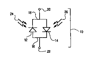
22 The opsistor (10) {Fig. 1) comprises two PIN photodiodes, the first
photodiode
7
CA 02274666 1999-06-10
WO 99/27589 PCT/US97/22229
( 12) and the second photodiode ( 14), electrically connected in an inverse
parallel
2 manner such that the anode of the first photodiode (12) is electrically
connected to the
cathode of the second photodiode ( 14) via a first common conductor ( 16), and
the
9 cathode of the first photodiode (12) is connected to the anode of the second
photodiode ( 14) via a second common conductor ( 18). The voltage phase
developed
s by the opsistor (10) is measured from the first output terminal (20) and the
second
output terminal (22). A first transmitter signal light source (24) to the
first photodiode
a (12) is represented by the arrows (24}. A second transmitter signal light
source (26) to
the second photodiode (14) is represented by the arrows (26). The voltage-
phase
io developed at the output terminals (20,22) is determined by which of the two
photodiodes ( 12,14) produces a higher voltage which is dependent on the
relative
i2 intensity of illumination they receive from the transmitter signal light
sources (24,26).
For example if the first photodiode ( 12) produces a higher voltage than the
second
i 9 photodiode ( 14), then the voltage phase measured from the first output
terminal (20)
will be negative and the voltage-phase from the second output terminal (22)
will be
~ s positive. On the other hand, if the voltage from the second photodiode (
14) is greater
than the voltage from the first photodiode ( 12), then the voltage-phase
measured from
is the first output terminal (20) will be positive and the voltage-phase
measured from the
second output terminal (22) will be negative. Thus if the two photodiodes
(12,14) are
2o sinular or identical as possible, the voltage-phase from the output
terminals (20,22) is
controlled by relative intensity of illumination of the two photodiodes, i. e.
changes in
22 the relative illumination from transmitter signal light sources (24,26) to
the two
photodiodes (12,14).
CA 02274666 1999-06-10
WO 99/27589 PCT/US97/22229
A preferred embodiment (Fig. 2) is a bandwidth-filtered opsistor ("the
2 OPS-F") (30). The OPS-F (30) comprises two PIN photodiodes (32,34), the
first
photodiode (32) filtered with the first bandwidth-portion filter (33), and the
second
photodiode (34) filter with the second bandwidth-portion filter (35),
electrically
connected in an inverse parallel manner such that the anode of the first
photodiode
s (32) is electrically connected to the cathode of the second photodiode (34)
via a first
common conductor (36), and the cathode of the first photodiode (32) is
connected to
a the anode of the second photodiode (34) via a second common conductor (38).
The
first bandwidth-portion filter (33) passes a different bandwidth of
transmitter signal
~. o light than the second wavelength-portion filter (3 5 ). The voltage-phase
developed by
the OPS-F (30) is measured from the first output terminal (40) and the second
output
i2 terminal (42). The first bandwidth-portion signal light source ("WPSLS-1
")(44) to the
first photodiode (32) is represented by the arrows (44). The second
i4 bandwidth-portion signal light source ("WPSLS-2")(46) to the second
photodiode (34)
is represented by the arrows (46). Because each wavelength-portion filtered
i6 photodiode (32, 34) responds only to its own specific bandwidth of light,
WPSLS-1
(44) for photodiode {32) and WPSLS-2 (46) for photodiode (34) can be provided
is from a distant location without cross-talk interference. The term "light"
is not
restricted to visible light, but also include wavelengths from the far
ultraviolet to the
2o far infrared.
The voltage-phase developed at the output terminals (40,42) is
z2 determined by which of the two photodiodes (32,34) produces a higher
voltage which
in turn is dependent on the relative illumination they receive from the
transmitter signal
9
CA 02274666 1999-06-10
WO 99/27589 PCT/US97/22229
light sources, WPSLS-1 (44) and WPSLS-2 (46). For example in Fig. 2, if the
first
2 photodiode (32) receives a greater illumination from WPSLS-1 (44) and thus
produces
a higher voltage than the second photodiode (34) being illuminated by WPSLS-2
(46),
then the voltage-phase measured from the first output terminal (40) will be
negative
and the voltage-phase from the second output terminal (42) will be positive.
On the
s other hand, if the second photodiode (34) receives a greater illumination
from
WPSLS-2 (46) and thus produces a higher voltage than the first photodiode (32)
s receiving illumination from WPSLS-1 (44), then the voltage-phase measured
from the
first output terminal (40) will be positive and the voltage-phase measured
from the
second output terminal (42) will be negative. Thus if the two photodiodes
(32,34) are
similar or identical, the voltage-phase from the output terminals (40,42) is
controlled
12 by relative illumination and changes in the relative illumination of WPSLS-
1 (44) and
WPSLS-2(46) to the two photodiodes {32,34).
1g Preferably, as shown in Figs. 3-4, the OPS-F device (30), is constructed
as a monolithic integrated circuit. The OPS-F (30) consists of two PIN
photodiodes
i6 (32,34), the first photodiode (32) filtered with the first bandwidth-
portion filter (33),
and the second photodiode (34) filter with the second bandwidth-portion filter
(35),
is electrically connected in an inverse parallel manner such that the cathode
(32c) of the
first photodiode (32) is electrically connected to the anode (34a) of the
second
2o photodiode (34) via a first common conductor (36), and the anode (32a) of
the first
photodiode (32) is connected to the cathode (34c) of the second photodiode
(34) via a
22 second common conductor (3$). The first bandwidth-portion filter (33)
passes a
different bandwidth of stimulating light than the second bandwidth-portion
filter (35).
CA 02274666 1999-06-10
WO 99/Z7589
PCT/US97/22229
The voltage-phase developed by the OPS-F (30) is measured from the first
common
2 conductor (36) and the second common conductor (38) which are also the
output
terminals. The voltage-phase developed at the common conductors (36,38) is
9 determined by which of the two photodiodes (32,34) produces a higher voltage
which
is dependent on the relative illumination which they receive from their
respective signal
s light sources.
For example if the illumination of the entire OPS-F (30) contains a
a greater proportion of bandwidths that can stimulate the first photodiode
(32) than can
stimulate the second photodiode (34), then a higher voltage will be developed
by the
io first photodiode (32) than the second photodiode (34), and the voltage-
phase
measured from the first common conductor (36) will be negative and the voltage-
phase
12 measured from the second common conductor (38) will be positive. On the
other
hand, if the illumination to the entire OPS-F (30) contains a greater
proportion of
i4 bandwidths that can stimulate the second photodiode (34) than can stimulate
the first
photodiode (32), then a higher voltage will be developed by the second
photodiode
i 6 (34) than the first photodiode (32), and the voltage-phase measured from
the first
common conductor (36) will be positive and the voltage-phase measured from the
is second common conductor (38) will be negative.
In the preferred embodiment of the OPS-F (30) shown in Figs. 3-4, the
2o P+ surface (40) of the first photodiode (32) has its anode (32a) deposited
around the
entire edge of the P+ region (40), and the cathode (32c) of the first
photodiode (32) is
22 deposited completely over a Iarge area of the N+ region (52) under the
cathode (32c).
Similarly in the preferred embodiment of the OPS-F (30) shown in FIG. 3, the
P+
11
CA 02274666 1999-06-10
WO 99/27589 PCTNS97/22229
surface (42) of the second photodiode (34) has its anode (34a) deposited
around the
2 entire edge of its P+ region (42), and the cathode (34c) of the second
photodiode (34)
is deposited completely over a large area of the N+ region (62) under the
cathode
q (34c}. The starting P-type silicon substrate (44) is shown surrounding the
two
photodiodes (32, 34). Although, the starting monolithic silicon substrate (44)
for the
illustrated preferred embodiment of the OPS-F device (30) of the present
invention is
undoped silicon (44), those skilled in the art will recognize that P-type or N-
type
s silicon may also be use as a starting monolithic silicon substrate by
altering the
fabrication of the OPS-F's photodiodes.
to As illustrated in Fig. 4, the construction of the OPS-F (30) follows
standard semiconductor fabrication processes. PIN photodiodes (32,34) each
with a
i2 distinct intrinsic layer (50,58) are used in this embodiment because of
their higher
switching speeds. A first heavily doped N-region (54) and a second heavily
doped
lq N-region (60) are fabricated in close proximity to each other in the
starting undoped
substrate (44). A first N+ region (52), and a second N+ region (62) are then
fabricated
1 s in the first N-region (54) and the second N-region (60) respectively. A
first heavily
doped P-region (48) and a second heavily doped P-region (56) are then
fabricated in
18 the first N-region (54) and second N-region (60) respectively. A first
intrinsic layer
(50) then forms at the junction of the P-region (48) and the N-region {54). A
second
2o intrinsic layer (58) then forms at the junction of the P-region (56) and
the N-region
(60). A first P+ region (40) is then fabricated in the first P-region (48),
and a second
22 P+-region (42) is then fabricated in the second P-region (56). A first
metallic anode
(32a) is deposited on the first P+ region (40) on its perimeter to permit a
large area of
12
CA 02274666 1999-06-10
WO 99/27589 PCT/US97/22229
electrical contact and a second metallic anode (34a) is deposited on the
second P+
2 region (42) on its perimeter to permit a large area of electrical contact. A
first metallic
cathode (32c) is deposited on the entirety of the first N+ region {52) to
permit a large
area of electrical contact. A second metallic cathode (34c) is deposited on
the entirety
of the second N+ region (62) to permit a large area of electrical contact. The
first
6 wavelength-portion filter (33), which in the preferred embodiment is a
multilayer
dielectric layer, is deposited on the first photodiode (32). The second
s wavelength-portion filter (3 5), which in the preferred embodiment is a
multilayer
dielectric filter, is deposited on the second photodiode (34).
1 o Filter layers (33,3 5) each pass a different bandwidth of light within the
spectrum from 450 nm to 1150 nm, the spectral response of silicon photodiodes.
In
i2 the preferred embodiment for example, the first filter layer (33) has a
bandwidth pass
from 600 nm to 850 nm, and the second filter layer (35) has a bandwidth pass
from
19 850 nm to 1100 nm. Those skilled in the art however will recognize that
other
bandwidths, both greater and smaller, are also useful.
i 6 A silicon dioxide insulating layer (70) is fabricated on the areas of the
OPS-F (30) not covered by the filter layers (33,35). Openings are etched in
filter
is layers (33,35) to exposed the anodes (32a, 34a) and the cathodes (32c,
34c). A first
common conductor (36) is then deposited to connect the first cathode (32c) to
the
ao second anode (34a), and a second common conductor (38) is deposited to
connect the
first anode (32a) to the second cathode (34c). The common conductors (36,38)
also
22 serve as the output terminals (42,40) illustrated in Fig. 2.
Figure 5 illustrates a TM2/OPS-F combination used for long-distance
13
*rB
CA 02274666 1999-06-10
WO 99/27589 PCTNS97/22229
open-air data transmission ("LDOADT") with characteristic high resistance to
2 background noise, and high data transmission rates. The TM2 (70) is provided
signal
coding and powered by the transmitter (72). The WPSLS-1(44) and the WPSLS-2
Q (46) of the TM2 (70) include LEDs, lasers, or any light source capable of
producing
specific bandwidths of light in a rapid pulsed manner. The TM2 digital signal
(78),
s comprised of the first bandwidth signal light ("WPSL-1) (74), and the second
bandwidth signal light ("WPSL-2") (76), is highly resistant to common mode
noise
s such as ambient light (80), 60 Hz interference (82), and atmospheric
attentuations
(84). The TM2 signal (78) is sensed by the OPS-F (30) and differentially
converted
io into positive or negative voltage-phase signals by the first photodiode
(32) and the
second photodiode (34) of the OPS-F (30). The voltage-phase developed by the
i2 OPS-F (30) is decoded and reconstructed by a receiver (86) in an industry
standard
manner.
19 For LDOADT applications employing the OPS-F embodiment of the
opsistor, by utilizing a different light bandwidth filter over each OPS-F
receiver
is opsistor photodiode, the two transmitter light sources of the TM2 (each
producing the
specified different bandwidths of light) may be located at a great distance
from the
is OPS-F receiver. In addition the OPS-F receiver may receive serial
communication
even though the OPS-F device is in motion, such as if placed on rapidly moving
2o equipment, or even if blocked by a light diffuser such as biological
tissue. For
example, in the latter case, by using red and infrared light as the two TM2
wavelengths
22 that penetrate the skin into subcutaneous tissues, a subcutaneously
implanted OPS-F
sensor may receive serial communications via an external TM2 transmitter to
provide
14
CA 02274666 1999-06-10
WO 99/27589 PCT/US97/22Z29
power and programming to an implanted drug delivery pump.
2 The advantages of the TM2/OPS-F combination device of this
invention for LDOADT are appreciated when compared to the current art for
4 LDOADT. Typically in the current art, a transmission LED is modulated at a
carrier
frequency approximately 15X higher than the target data rate or baud rate. For
6 example, in remote control and low speed serial PC-IR links, a carrier
frequency of
about 38 KHz is used to transmit signal bursts to the receiver. The presence
of a burst
is interpreted as one logic state and the absence its compliment. By timing
the signal
burst properly in real time, an equivalent data rate of 300 to 2400 baud can
be reliably
io achieved. Newer standards today for PCs have improved this data rate to
over 100
kilobits per second but the working distance is just a few feet.
12 Signal integrity between transmitter and receiver must negotiate
ambient light levels and changing attenuation. Even with bandpass filters and
signal
19 processing, the transmission rates must be compromised to obtain the
required signal
to noise margin over background. Signal variations from ambient behave similar
to
i s dynamic voltage offsets to the IR carrier signal and can be categorized as
"noise."
Depending on the receiver circuit, the maximum data rate reliably received is
limited by
i s the signal to noise ratio possible, the better the quality of the incoming
signal, the
faster will be the possible data rate. With open air applications ambient
noise is highly
2 o dynamic, and ample guardband is reserved to ensure reliable data
transmission under
all conditions.
22 Using the TMZ/OPS-F transmitter-receiver combination for LDOADT
applications, instead of ,for example, an intensity amplitude modulated
transmitter
CA 02274666 1999-06-10
WO 99/Z7589 PCT/US97/22229
LED and a single photodiode receiver, the TMZ/OPS-F combination uses an active
2 wavelength alternation method utilizing two separate color LEDs for
transmitting logic
ones and zeros to produce a voltage-phase modulation. This TM2 bi-phasic drive
system transmits two wavelengths alternately to produce the effect of a
carrier signal at
the OPS-F receiver. For example, if GREEN and RED were the two bi-phasic
wavelengths, GREEN is ON during the positive excursion of the carrier and RED
is
ON during the negative excursion of the carrier. These PUSH-PULL excursions
are
a recognized as positive or negative voltage-phases at the OPS-F. This bi-
phasic
approach forces all ambient factors to become common mode and therefore become
Zo automatically canceled at the OPS-F input. Normal signal processing now
converts
the Garner into a digital data stream. A gain of better than 20 dB in SIN is
obtained
i2 with the TM2/OPS-F combination. Faster data transmission and longer
transmitter-receiver distances are obtainable.
14 Figure 6 illustrates a TM2/OPS-F combination used for High-Speed
Fiber Optic Data Transmission ("HSFODT") with characteristic high data
transmission
i s rates, and high resistance to fiber attenuations. The TM2 (70) is provided
signal
coding and powered by the transmitter (72). The WPSLS-1(44) and the WPSLS-2
is (46) of the TM2 (70) include LEDs, lasers, or any light source capable of
producing
specific bandwidths of light in a rapid pulsed manner. The TM2 digital signal
(78)
2o comprised of the first bandwidth signal light ("WPSL-1 ") (74) and the
second
bandwidth signal light ("WPSL-2") (76) is highly resistant to fiber
attenuations such as
22 from temperature effects, mechanical stress, impurity/defect effects, and
water
absorption during passage through the conduit optical fiber (88). The TM2
signal (78)
16
CA 02274666 1999-06-10
WO 99/27589 PCT/US97/22229
is sensed by the OPS-F (30) and differentially converted into positive or
negative
2 voltage-phase signals by the first photodiode (32) and the second photodiode
(34) of
the OPS-F (30). The voltage-phase developed by the OPS-F (30) is decoded and
reconstructed by the receiver (86) in an industry standard manner.
The advantages of the HSFODT use of this invention are apparent from
s comparing it against current art technology. In the current art, a laser
source is use to
serially transmit monochromatic light signals through an optical fiber to a
PiN or
a avalanche type photodiode detector. Data rates from 20 Mbits/second to
Gigabits/second are possible with the proper combination of optics and
electronics.
io With high end applications like telecommunication, factors such as
wavelength
selection, multimode fibers, low loss connectors, repeaters, and low noise
detectors are
i2 optimized to achieve the best possible performance. This performance,
however, can
be further improved if factors such as temperature stress, mechanical stress,
and fiber
i4 imperfections can be converted into common mode parameters.
By utilizing bi-phasic TMZ drive and OPS-F bi-phasic opsistor
i s detection, the S/N ratio of a fiber link can be improved upon compared to
the current
art. This increase allows the use of longer span distances between repeaters
and/or
is increased data transmission rates. The majority of noise variables within a
fiber are
predominantly single-ended or ground referenced. An example is attenuation
2 o variations from micro mechanical stresses along a fiber experiencing
temperature
fluctuations or vibration. The TM2/OPS-F combination used for HSFODT permits
22 balanced signal detection around zero volts. In this approach, a positive
voltage vector
is a Logic One while a negative voltage vector is a Logic Zero. A DC-coupled
17
CA 02274666 1999-06-10
WO 99127589 PCTlUS97/22229
amplifier can be used that eliminates many capacitor-related issues (e.g.,
phase and
2 time delays) for processing ultra-fast signals. Balanced detection also
eliminates the
need to store a reference voltage (usually by a capacitor) needed to compare
input
4 signals against to test for Logic 1 or Logic 0. Higher data transmission
rates can be
achieved that increase the information bandwidth of a fiber.
With lower technology applications such as computer network fiber
links, improvements in the signal-to-noise ratio will allow greater tolerance
to fiber
s imperfections. This in turn can lower fiber cost for consumer applications.
One such
application may be usage of a lower grade fiber for connection into single
family
io homes that satisfies the required data bandwidth but has higher cost
effectiveness.
Figure 7a is a is a cross-sectional diagram of a TM2/OPS-F monolithic
12 optical fiber link used in an optoelectronic based state machine. The TMZ
(70), which
preferably is composed of amorphous silicon LEDs, is fabricated within the
monolithic
19 silicon substrate (92). Similarly, the OPS-F (30) is also fabricated within
the
monolithic silicon substrate (92) using techniques standard to the industry.
Digital
i6 informational data is optically transmitted from a TM2 (70) to a target OPS-
F (30) via
a micro-optical fiber light conduit (90) fabricated upon the silicon substrate
(92) using
18 standard industry techniques.
Figure 7b illustrates a laser write of a OPS-F subunit (30a) disposed as
20 one of a plurality of OPS-F subunits (30) on a monolithic silicon substrate
(92). The
OPS-F (30) is used as the basic switch component of an optoelectronic based
state
22 machine. Because of direct optical access, the TM2 laser beam (94) can
rapidly write
changes to the voltage-phase state of a large number of OPS-Fs (30) converting
them
18
CA 02274666 1999-06-10
WO 99/Z7589 PCT/US97/22229
to one of three OPS-F electrical tri-states.
2 The OPS-F based optoelectronic state machine functions in the
following manner. In general, a state machine performs a specific function
determined
9 by its configuration, which can be actively changed. Field programmable
logic silicon
devices such as gate arrays, and one-time programmable devices are state
machines
s that can be reconfigured to meet many different applications. In the case of
a
UV-erasable OTP, the computer chip is "dormant" after erasure but becomes
s functional again after reprogramming. The OPS-F device of this invention
also has a
"dormant" null state that is analogous to the "OFF" position of a mechanical
center-off
io toggle switch. When OPS-F receiver is activated by TM2 light transmission,
the
switch can "toggle" to the UP or DOWN position for logic 1 (positive voltage
vector)
i2 or logic 0 (negative voltage vector) respectively. Once programming is
complete, the
switch goes back to the center or "OFF" state (ground, 0 volts). This OPS-F
tri-sate
14 capability, therefore, allows an OPS-F based optoelectronic state machine
to possess
three states, represented by a positive voltage vector, a negative voltage
vector, and a
1 s ground, 0 volts null.
With the OPS-F based optoelectronic state machine, the OPS-F is the
is input to a configuration FIFO (First In First Out) latch that defines the
functionality of
that state machine block, or the function of an OPS-F is latched in a high or
low logic
2o state which in turn "steers" the processing logic of the state machine.
Since the OPS-F
normally has a rest state that is not a logic 1 or logic 0, immunity to noise
after
22 configuration is very high. By using bi-phasic TM2 light transmission from
an external
source such as two laser sources or a tunable laser, or from another section
of the state
19
CA 02274666 1999-06-10
WO 99/27589 PCT/US97/22229
machine, the entire state machine can be quickly reprogrammed for
functionality as the
2 situation requires. Permitting different optoelectronic blocks to change
personality or
function on-the-fly minimizes the hardware required for a OPS-F based state
machine
9 {vs. traditional microprocessors that are composites of predefining
functional blocks).
The OPS-F "building block" permits integration of many "smart state machine"
blocks
s based on using bi-phasic TM2 light as the primary link. In this approach,
traditional
requirements for serial communications, signal multiplexing, and device
programming
s are minimized, since a "smart state machine" block can, for example, change
from a
"division fianction" to a "counter function" on-the-fly.
to Advantages of such a "smart state machine" block based on the
TMZ/OP S-F combination over the present art include: ( 1 ) faster optocoupler
12 transmission data rates from the active on/active off function, (2) direct
laser writes
into specific parts of the "smart state machine" to program "smart state
machine"
i 4 blocks circumvents the complexities of serial communications and signal
action
routing. The steering of the lasers is equivalent to traditional functions of
wires and
i s logic clocks resulting in faster operation since silicon elements do not
have to be
physically close but may be separated, (3) applications in bio-sensor devices
where
18 fluids may surround the silicon, and (4) field programmable devices where
isolation
preservation is important.
2o Figure 8 (OPTICAL QUADRATURE ENCODER) illustrates the
opsistor device of this invention used in place of standard photodiode
detectors
22 employed in an optical encoder to double the resolution of the encoder
without
increasing the slot count of the rotor disk. The photo-sensing portion ( 1 O 1
) within an
CA 02274666 1999-06-10
WO 99.27589 PCT/US97/22229
optical encoder utilizing the device of this invention, employs a first
opsistor (30) and a
2 second opsistor (100) as the photodetectors. The first opsistor (30) has a
first
photodiode subunit (32), designated "C", and a second photodiode subunit (34)
4 designated "D". The second op sistor ( 100) has a first photodiode subunit (
102)
designated "E", and a second photodiode subunit (104) designated "F".
Illumination
6 (112) to the opsistors (30, 100) passes through the rotor slots (106)
created between
the rotor vanes (108). Movement of the rotor in FIG. 8 is shown by the arrow
(110).
s The 2X resolution quadrature signal of the photo-sensing portion ( 1 O 1 )
of the opsistor
based encoder results because the rotor slots ( 106) of the optical encoder
section ( 1 O I )
io are each effectively split into two portions by each of the opsistors (30,
100). As the
illumination (112) from the rotor disk slots (106) passes over the first
photodiode
i2 subunit (32, 102) of either opsistor (30, 100) a voltage-phase in one
direction will
developed in that respective opsistor. As the illumination (112) from the
rotor disk
slots (106) continues to move over the entirety of either opsistor surface and
illuminates both of the photodiode subunits (32 and 34, or 102 and 104), a
is voltage-phase null will occur. When the illumination (112) from the rotor
disk slots
(106) begin to pass preferentially over the second photodiode subunit (34,
104) of
is either opsistor (30, 100), the voltage-phase will become inverted to the
opposite
direction. The slot widths ( 106) are thus functionally split into two
portions each. A
2 o two-slot, two-opsistor quadrature encoder can achieve twice the resolution
of the
same encoder using two standard photodiodes.
22 Figures. 9a-9c illustrate the opsistor of the present invention used as a
precise linear optical position sensor ("LOPS"). In FIG. 9a, a null of the
voltage-phase
21
CA 02274666 1999-06-10
WO 99/27589 PCTNS97/22229
develops when the illumination (94) of the two photodiode subunits (32, 34) of
the
2 opsistor (30) is equal. A rapid shift of the voltage-phase to positive or
negative
develops in a flip-flop manner as soon as one of the two opsistor photodiode
subunits
(32, 34) become preferentially illuminated as shown in FIGs. 9b and 9c. As the
voltage-phase of the opsistor (30) responds to light balance only over its two
s photodiode subunits (32, 34) which may be fabricated together very closely
on a
monolithic silicon substrate, the opsistor's rejection of common mode
attenuations
a such as ambient light and temperature effects is high. Uses of a LOPS device
such as
that shown include micro-beam balances, optical alignment applications, motion
io sensors, and image recognition devices based on edge detection.
Figures 10 A-C illustrate a two-dimensional target sensor (130)
i2 constructed from two "stacked" LOPS opsistors (110, 120) aligned so that
the "top"
LOPS opsistor (110), consisting of photodiode subunits (112, 114), which is
fabricated
14 within a thin silicon substrate transparent to infrared light, is aligned
at 90 degrees
rotated from the "bottom" LOPS opsistor (120), consisting of photodiode
subunits
is (122, I24). Such a target sensor (130) uses one LOPS opsistor sensor (110,
120) for
each axis of position sensing of a light target (94). Characteristics and
quality of such
i a a two-dimensional target sensor ( 13 0) include simple fabrication and
minimal
dead-spot area, in additional to all of the characteristics of the single LOPS
sensor.
2o Uses of such a LOPS device include those requiring high precision two-
dimensional
alignment, weapons targeting, spectrophotometer micro-two-dimensional
alignments,
22 and micro-machine/micro-fabrication jig alignment.
22